Note: Descriptions are shown in the official language in which they were submitted.
CA 02244044 2000-07-25
1
CURRENT MODE CONTROLLER FOR CONTINUOUS CONDUCTION MODE
POWER FACTOR CORRECTION CIRCUIT AND METHOD OF OPERATION
THEREOF
Technical Field of the Invention
The present invention is directed, in general, to power
conversion and, more specifically, to a current node
controller for a power factor correction circuit operating
in a continuous conduction mode (CCM) that handles a
relatively wide range of AC input voltages and a method of
operating a current mode control in CCM to achieve power
factor correction.
Background of the Invention
Over the past ten years, substantial efforts have been
dedicated to the design of controllers for switching power
supplies required to provide electrical power having both a
high power factor and low total harmonic distortion (THD).
One objective in designing such controllers has been to
distort as little as possible the AC line current that is
provided to such switching power supplies.
For a time, it was believed that the International
Electronic Commission would subject electrical equipment,
such as computers and communication devices, to a proposed
standard IEC-555, which called for THD limits as low as 5%.
However, the IEC never adopted IEC-555, opting instead to
approve IEC-1000.3.2 imposing less-rigorous THD limits.
For power supplies operating at about 1.5 kW (at 110
VAC or about 3 kW at 220 VAC), IEC-1000.3.2 limits the
allowable input current THD to 5%, as did the proposed IEC-
555 standard. However, for power supplies operating
below600 W, the IEC-1000.3.2 standard allows THD of up to
30%.
Peak current mode control and average current mode
control are two well-known, alternative approaches to
regulating the output voltage of switching power supplies to
CA 02244044 2000-07-25
2
achieve high power factor. Presently, the industry-
preferred approach is average current mode control.
In conventional average current mode control, the
control voltage (representing an error between the actual
output voltage and a reference voltage) is used to produce a
reference current to modulate a desired input current.
Therefore, the control voltage directly controls the output
voltage. Ideally, the control voltage in the conventional
average current mode controller directly controls the
average value of the current passing through the inductor
for the fastest response.
Unfortunately, the conventional average current mode
control is more complex and expensive to implement than is
alternative peak current mode control. Additionally, high
power factors and lower THD are attainable using peak
current mode control for narrow input voltages and load
variations. See "An Overview of Power Factor Correction in
Single-Phase Off-Line Power Supply Systems" by J. Sebastian,
et al., IECON94 Proceedings.
In peak current mode control, the switch or inductor
current is compared with a threshold signal. THD of less
than 5o is realizable if the parameters of the ramp waveform
are appropriately selected for the particular line current.
Peak current mode control, however, has difficulties in
providing low line current distortions over a wide range of
AC input voltages and output loads.
Various enhancements extending the circuit design of
basic peak current mode control have attempted to adjust the
circuit parameters of the ramp waveform to extend the
practical operating range of peak current mode control.
These enhancements include feed-forward from the rectified
AC line voltage to correct the parameters of the ramp
waveform. Another approach uses the output of the voltage
amplifier to correct the ramp, so as to increase the
practical range of operation in discontinuous conduction
CA 02244044 2000-07-25
3
mode (DCM). See, "Power Factor Correction Using a
Preregulating Boost Converter" by L. Hadley, Power
Conversion Proceedings, October 1989, pp. 376-382, and
"Reducing Distortion in Boost Rectifiers with Automatic
Control" by R. Redl, Applied Power Electronics Conference
Proceedings, 1997, pp. 74-80.
However, the techniques and enhancements described in
the above-mentioned publications are only applicable to
converters, i.e., boost converters, operating in DCM.
Similar problems and limitations faced by converters
operating in continuous conduction mode (CCM) are not
addressed. Furthermore, although those techniques discussed
above have been able to improve the operating range of the
power factor correction stage in DCM of operation, there are
still regions of very high THD (greater than 400) for power
supplies required to operate from 85 VAC to 265 VAC
(commonly known as "universal input").
Accordingly, what is needed in the art is an
improvement to current mode control that permits CCM
operation and provides lower THD over a wider range of input
voltages and load variations
Summary of the Invention
To address the above-discussed deficiencies of the
prior art, the present invention provides, for use with a
power factor correction circuit operable in CCM, a current
mode controller, a method of operating a power factor
correction circuit to achieve current mode control thereof
and a power supply incorporating the controller or the
method. In one embodiment, the controller includes: (1) a
modulator, coupled to a switch in the power factor
correction circuit, that senses an electrical characteristic
and a current passing through the power factor correction
circuit and provides, in response thereto, a control signal
to the switch and (2) a compensation circuit, coupled to the
CA 02244044 1998-07-28
4
power factor correction circuit, that provides a
compensation signal to the modulator that is a function of
a rectified line voltage provided to the power factor
correction circuit. The compensation signal causes the
S modulator to modify the control signal to reduce a THD of
the power factor correction circuit.
The present invention introduces the broad concept of
employing a harmonic component present in the rectified AC
line voltage provided to the power factor correction
circuit, in combination with the sensing of a current in the
power factor correction circuit, to modify the control
signal provided to the switch in the power factor correction
circuit. This serves to compensate for variations in input
voltage and reduce the THD of the power factor correction
circuit.
In one embodiment of the present invention, the
electrical characteristic is an output voltage of the power
factor correction circuit. Those skilled in the art will
recognize, however, that control based on other than the
output voltage may be advantageous in certain applications.
In one embodiment of the present invention, the
compensation circuit comprises a capacitor coupling the
input of the power factor correction circuit to the
modulator. The capacitor, while not necessary to the
present invention, provides sign and phase adjustment to the
compensation signal.
In one embodiment of the present invention, the
modulator comprises an amplifier and a feedback path
coupling an output of the amplifier to an input thereof, the
feedback path including a capacitor. The capacitor in the
feedback path acts as an integrator, generating a feedback
compensating signal that governs transitions in the control
signal.
In one embodiment of the present invention, the
compensation signal is dependent on the value of a capacitor
in the compensation circuit. In an embodiment to be
CA 02244044 1998-07-28
illustrated and described, the capacitor in the compensation
circuit modifies the effective slope of the ramp that the
capacitor in the modulator creates by integration.
In one embodiment of the present invention, the control
5 signal is a function of an input inductor current. In
alternative embodiments to be illustrated and described, the
control signal may be created by other than directly sensing
the input inductor current.
In one embodiment of the present invention, the
controller further comprises an input voltage detection
circuit that senses a rectified voltage provided to the
power factor correction circuit and modifies the control
signal as a function thereof. Alternatively, a circuit may
sense an error signal in the modulator and modify the
control signal as a function thereof. One way to modify the
control signal is to modify a resistance in the modulator.
In an embodiment to be illustrated and described, the
input voltage detection circuit divides the range of input
voltage into two sub-ranges and changes the resistance in
the modulator depending upon whether the input voltage is in
one sub-range or the other. This effectively changes the
amplitude of the current signal fed back to the modulator to
adapt to the particular sub-range encountered. Of course,
other embodiments may provide more than'two sub-ranges or a
continuously variable ramp slope.
The foregoing has outlined rather broadly the features
and technical advantages of the present invention so that
those skilled in the art may better understand the detailed
description of the invention that follows. Additional
features and advantages of the invention will be described
hereinafter that form the subject of the claims of the
invention. Those skilled in the art should appreciate that
they may readily use the conception and the specific
embodiment disclosed as a basis for modifying or designing
other structures for carrying out the same purposes of the
present invention. Those skilled in the art should also
CA 02244044 1998-07-28
6
realize that such equivalent constructions do not depart
from the spirit and scope of the invention in its broadest
form.
Brief Description of the Drawincrs
For a more complete understanding of the present
invention, reference is now made to the following
descriptions taken in conjunction with the accompanying
drawings, in which:
FIGURE 1 illustrates a schematic diagram of a switching
power supply employing an embodiment of a current mode
controller constructed according to the principles of the
present invention;
FIGURE 2 illustrates a schematic diagram of a switching
power supply employing an embodiment of a current mode
controller constructed according to the principles of the
present invention;
FIGURE 3 illustrates another embodiment of the current
mode controller of FIGURE 2 incorporating an embodiment of
a voltage range detection circuit constructed according to
the principles of the present invention;
FIGURE 4 illustrates a schematic diagram of a switching
power supply employing an embodiment of a current mode
controller controlling based on inductor current according
to the principles of the present invention;
FIGURE 5 illustrates a schematic diagram of a switching
power supply employing an embodiment of a current mode
controller and incorporating an embodiment of an input
voltage detection circuit constructed according to the
principles of the present invention;
FIGURE 6 illustrates a schematic diagram of a switching
power supply employing an embodiment of a current mode
controller with low/high line detection constructed
according to the principles of the present invention;
FIGURE 7A illustrates an optimum ramp injection as a
function of the root-mean-square (rms) input line voltage;
CA 02244044 1998-07-28
7
FIGURE 7B illustrates a two-level approximation of an
optimum ramp injection as a function of the input line
voltage; and
FIGURE 7C illustrates a two-line approximation of an
optimum ramp injection as a function of the line voltage.
Detailed Description
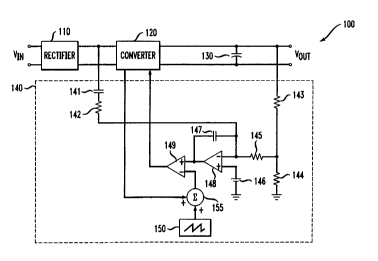
Referring initially to FIGURE 1, illustrated is a
schematic diagram of a switching power supply 100 employing
an embodiment of a current mode controller 140 constructed
according to the principles of the present invention. The
switching power supply 100 includes a rectifier 110 that is
coupled to a converter 120. The converter 120 (one
embodiment of a power factor correction circuit, and which
may be, for instance, a boost power factor correction
converter) is also coupled to an output capacitor 130. Also
shown is the current mode controller 140 that is coupled to
the rectifier 110, converter 120 and the output capacitor
130. The rectifier converts AC power into rectified power
having a harmonic current component.
The current mode controller 140 includes a modulator
and a compensation circuit. The mode controller 140
includes a first and second resistor 143, 144 that make up
a voltage divider circuit. A third resistor 145 is coupled
to the first and second resistors 143, 144 and to an
inverting input of a voltage-feedback operational amplifier
(op-amp) 148. An integrating capacitor 147 is coupled (in
a feedback path) between the inverting input and the output
of the voltage-feedback op-amp 148. Those skilled in the
art should be aware that although a capacitor is used in the
feedback circuit of the voltage-feedback op-amp 148, other
circuit feedback configurations may also be used. The non-
inverting input of the voltage-feedback op-amp 148 is
coupled to a reference voltage 146. The output of the
voltage-feedback op-amp 148 is coupled to the non-inverting
input of a comparator op-amp 149. The output of the
CA 02244044 1998-07-28
8
comparator op-amp 149 is coupled to a switch (not shown) in
the converter 120 and the inverting input of the comparator
op-amp 149 is also coupled to the converter 120 and a
summing node 155. The summing node 155 is coupled to an
external ramp waveform generator 150. The modulator, in the
illustrated embodiment, includes the resistors 143, 144,
145, the voltage reference 146, the integrating capacitor
147, the op-amps 148, 149, the summing node 155 and the ramp
generator 150. The compensation circuit includes a
compensating capacitor 141 coupled in series with a
compensating resistor 142. Typically, the compensation
circuit should be similar to the feedback circuit (the
integrating capacitor 147) of the voltage-feedback op-amp
148. The compensation circuit is coupled to a node (shown,
but not referenced) between the rectifier 110 and the
converter 120 and to the modulator.
The operation of the current mode controller 140 will
hereinafter be described. The output voltage of the
converter 120 is sensed by the voltage divider circuit
(including the first and second resistors 143, 144) and a
fixed proportion of the sensed output voltage is applied to
the inverting input of the voltage-feedback op-amp 148. The
rectified line voltage at the output of the rectifier 110 is
also sensed and a proportional value of'the sensed rectified
line voltage is injected into the inverting input of the
voltage-feedback op-amp 148. The rectified Line voltage
contains a distinct 2nd order (e.g., 120 Hz for a 60 Hz
input line) harmonic current component that can be used to
compensate and modulate the pulse width modulation (PWM)
signal to increase the duty cycle when the rectified line
voltage is close to the cross-over points and, conversely,
to decrease the duty cycle when the rectified line voltage
is at its-peak. By controlling the duty cycles, the cross-
over distortions can be minimized as the line voltage
increases. The sensed rectified line voltage is coupled
through the compensating capacitor 141 to obtain the proper
CA 02244044 1998-07-28
9
sign and phase at the output of the voltage-feedback op-amp
148. The 2nd line harmonic voltage component present in the
output voltage also contributes to the amount of 2nd line
harmonic voltage component present at the output of the
voltage-feedback op-amp 148. Also, a percentage of the
voltage-feedback op-amp 148 output signal that is from the
voltage feedback loop is 180 degrees phase shifted relative
to the signal fed forward through the integrating capacitor
147. The effect of the line and load variations can be
minimized by adjusting the contributions of the sensed
rectified line and output voltage signals. The output
signal of the voltage-feedback op-amp 148 is compared to a
signal composed of the sensed converter switch current and
the ramp waveform generated by the ramp generator 150. The
resulting signal at the output of the comparator op-amp 149
is used to control the duty cycle of the switch in the
converter 120.
Turning now to FIGURE 2, illustrated is a schematic
diagram of a switching power supply 200 employing an
embodiment of a current mode controller 240 constructed
according to the principles of the present invention. The
switching power supply 200 includes a rectifier 210 that is
coupled to a converter 220. The converter 220 is coupled to
an output capacitor 230 and to the current mode controller
240.
The converter 220 includes an inductor 221 coupled to
a converter diode 222. The converter diode 222 is also
coupled to a converter switch 224, typically a transistor,
and to the output capacitor 230. The converter switch 224
is coupled to a sensing resistor 225 that is coupled to the
current mode controller 240. Also shown is a converter
resistor 223 that is coupled to the converter switch 224 and
to the current mode controller 240.
The current mode controller 240 includes a modulator
and a compensation circuit. The compensation circuit
comprises a compensating capacitor 241 and a compensating
CA 02244044 2000-07-25
resistor 242 that are coupled to a node at the output of the
rectifier 210. Also shown is a voltage divider circuit of a
first and second resistors 243, 244 that are coupled to the
output capacitor 230. A current mode controller integrated
5 circuit (IC) 259 (e. g., UC 3843) is provided with a third
resistor 245 coupled in series with a second controller
capacitor 256 that is connected to the IC 259 COMP pin. The
third resistor 245 is used to provide a signal, proportional
to the output voltage of the converter 220, to the VFB pin
10 of the IC 259. A controller diode 250 is coupled to the
converter resistor 223 and to the IC 259 VOUT pin that
provides a signal that is used to control the converter
switch 224. A fourth resistor 251 is coupled between the IS
pin of the IC 259 and the sensing resistor 225 to provide
the converter switch 224 current signal to the current mode
controller 240. A controller transistor 252 is coupled to a
fifth resistor 253 coupled between the emitter of the
controller transistor 252 and to the IS pin of the IC 259.
The controller transistor 252 collector is coupled to a
sixth resistor 257 that is connected to the VREF pin of the
IC 259. The base of the controller transistor 252 is
coupled to a fourth capacitor 255 that is connected to the
IC 259 IS pin. A seventh resistor 258 also couples the base
of controller transistor 252 to the IC 259 VREF pin. The
controller transistor 252 in combination with the fifth
resistor 253 and the fourth capacitor 255 provide the ramp
shifting circuit used to control the converter switch 224.
The capacitor 255 is used to reset the current ramp. A
third capacitor 254 is coupled between the IC 259 RT/CT and
GND pins. A first and a second capacitor 261, 262 are
coupled to signal ground and to the IC 259 VREF and VCC
pins, respectively, providing filtering of the IC 259 input
bias supply voltage VCC.
The switching power supply 200 is operated with an
input voltage ranging from 85 VAC to 260 VAC, an input power
of approximately 570 Watts and an output voltage Vo of 397
CA 02244044 1998-07-28
11
VDC. The THD of the line current for the different line and
load conditions are summarized in Table I below.
Input VAC (V) Power input(W) Io (A) THD (~)
100 577 1.3 11.29
100 226 0.5 28.9
130 563 1.3 20.9
130 226 0.5 37.83
208 554 1.3 22.56
208 225 0.5 31.07
230 549 1.3 21.57
230 224 0.5 39.43
Table 1. Llne Current THD
Table I illustrates that the operation of the switching
power supply 200 employing the control technique of the
present invention over the universal input (i.e., 85 to 265
VAC) results in a THD of less than 40% over the entire
range.
The switching power supply 200, however, is typically
required to operate for an input voltage ranging from 68 VAC
to 265 VAC. For the switching power supply 200 to maintain
the low line current distortion, the input AC voltage range
should be taken into account by the current mode controller
240.
Turning now to FIGURE 3, illustrated is another
embodiment of the current mode controller of FIGURE 2
incorporating an embodiment of a voltage range detection
circuit 310 constructed according to the principles of the
present invention. The switching power supply 300 is
analogous to the switching power supply 200 except that the
voltage range detection circuit 310 is added. The voltage
range detection circuit 310 detects the AC voltage range and
modifies the signal level of the sensed converter switch 224
current being fed back to the current mode controller IC
CA 02244044 1998-07-28
12
259.
The voltage range detection circuit 310 includes a
ninth resistor 311 that is coupled to a tenth resistor 312.
The ninth and tenth resistors 311, 312 are also coupled to
an opto-coupler 320 (e. g., Model No. CNY-17, as manufactured
by Philips or Siemens) that is coupled to a voltage
detection transistor 318. The emitter of the voltage
detection transistor 318 is coupled to the opto-coupler 320
and the voltage detection transistor 318 collector is
coupled to a bias supply voltage VCC. An eleventh resistor
313 is coupled to a fifth capacitor 319 and to the opto-
coupler 320. A detection diode 317 is coupled in series with
a resistor 314 to the base of the voltage detection
transistor 318. A thirteenth and fourteenth resistors 315,
316 are coupled to the converter inductor 221 and form a
voltage divider that senses the rectified input voltage.
The opto-coupler 320 is used to add the ninth resistor
311 in parallel with the fourth resistor 251 to scale the
sensed converter switch 224 current. The THD of the line
current for different line and load conditions and an output
voltage Vo of 399 VDC are summarized in Table II below.
Input VAC (V) Power input(W) Io (A) THD
100 578 1.3 3.59
100 _ 231 0.5 10.64
100 144 0.3 20.13
130 567 1.3 4.37
130 229 0.5 24.87
130 144 0.3 33.98
210 556 1.3 11.49
210 226 0.5 32.48
210 142 0.3 31.06
230 551 1.3 18.05 i
230 224 0.5 37_54
CA 02244044 1998-07-28
13
230 ~ 141 ~ 0.3 I 34.34
Table II. Input Line Current THD
Table II illustrates that the effect of the line and load
variations on the generated line current harmonic components
are further minimized when the input line voltage is
considered by the current mode controller 240.
The level of the sensed line current varies according
to the following equation:
Iac - Pin ~ Vac ( 1 )
where Ia~ is the rectified line current, Pin is the average
input power and Va~is the root-mean-square (rms) input line
voltage. The average input power Pin can be assumed to be
constant, whereas the level of the signal fed forward from
the rectified line voltage is directly proportional to the
line voltage. Attempting to cancel the distortions due to
the line voltage variations results in over-modulation of
the line current at higher line voltages, typically greater
than 240 VAC. The over-modulation can be minimized by
sensing the converter inductor 221 current as opposed to the
converter switch 224 current and then filtering the sensed
signal before it is added to the external ramp waveform from
the waveform generator.
Turning now to FIGURE 4, illustrated is a schematic
diagram of a switching power supply 400 employing an
embodiment of a current mode controller 440 controlling
based on inductor current according to the principles of the
present invention. The switching power supply 400 is
analogous to the switching power supplies 100, 200
illustrated in FIGUREs 1, 2 with the difference being that
a current of a converter inductor 421, as opposed to the
converter switch 224, is sensed and filtered.
The switching power supply 400 includes an additional
second and third filtering resistors 450, 460 and a filter
capacitor 430. A sensing resistor 425 is now coupled
between a rectifier 410 and a converter 420 and is used to
CA 02244044 1998-07-28
14
sense the converter inductor 421 current instead of the
converter switch 224 current. The sensed converter inductor
421 current is then filtered by the filter capacitor 430
prior to being applied to a summing node 455. By filtering
the sensed current of the converter inductor 421, the signal
level that is fed forward from the rectified line voltage
can be increased without the penalty of over-modulation at
the higher input line voltages. Eliminating the over-
modulation problems at the higher line voltages results in
the decrease of the THD over the entire range of input line
voltages. The same result from filtering the converter
inductor current can also be realized with the use of a
"swinging" inductor in the boost stage of the converter. An
inductor constructed with a powdered iron core that is
allowed to saturate approximately 40 to 60% yields a
swinging inductor.
Turning now to FIGURE 5, illustrated is a schematic
diagram of a switching power supply 500 employing an
embodiment of a current mode controller and incorporating an
embodiment of an input voltage detection circuit 510
constructed according to the principles of the present
invention. The switching power supply 500 is analogous to
the aforementioned switching power supplies with the
exception that the input voltage detection circuit 510 is
incorporated to change the level of a sensed inductor
current fed back to the current mode controller. The -
modification of the sensed inductor current is based on the
range of an input line voltage. The input voltage detection
circuit 510 includes a first and second detection resistors
520, 530 that are coupled to a detection filter capacitor
540. A sensing resistor 525 is coupled between a rectifier
505 and a converter 507 to sense a converter inductor
current. The detection filter capacitor 540, used to filter
the sensed input voltage, is coupled to a detection switch
controller 560. The detection switch controller 560 is
coupled to a detection switch 580 (e.g., transistor) that is
CA 02244044 2000-07-25
coupled to a third and fourth gain controlling resistors
550, 570. The third and fourth gain controlling resistors
550, 570 are coupled to a summing node 555. The summing
node 555 is coupled to the inverting input of a comparator
5 op-amp 549 and a ramp generator590.
The sensed input line voltage is provided to the
detection switch controller 560 that determines whether the
detection switch 580 is turned ON or OFF. The detection
switch 580 is used to configure the resistive path of the
10 sensed inductor current to the comparator op-amp 549. The
detection switch controller 560 decides the signal path
based on the value of the input line voltage, resulting in
a low input line or high input line voltage mode of
operation. The third and fourth gain controlling resistors
15 550, 570 accordingly modifies the sensed inductor current
signal. By selectively using a different resistive value
based on the input line voltage to change the level of the
sensed inductor current, the THD over the entire input line
voltage range can be minimized. Turning now to FIGURE 6,
illustrated is a schematic diagram of a switching power
supply 600 employing an embodiment of a current mode
controller 640 with low/high line detection constructed
according to the principles of the present invention. The
switching power supply 600 includes a rectifier 610 that is
coupled to a converter 620. The converter 620 is coupled to
a output capacitor 615, sensing resistor 630 and a converter
inductor 625. Also shown is a current mode controller 640
with low/high line detection that is coupled to the
rectifier 610, converter 620, output capacitor 615, sensing
resistor 630 and converter inductor 625.
The current mode controller 640 with low/high line
detection includes a first and second resistor 641, 642 that
make up a voltage divider circuit. A third resistor 643 is
coupled to the first and second resistors 641, 642 and to an
inverting input of a voltage-loop error operational
amplifier (op-amp) 646. An integrating capacitor 645 is
CA 02244044 1998-07-28
16
coupled (in a feedback path) between the inverting input and
the output of the voltage-loop error op-amp 646. The non-
inverting input of the voltage-loop error op-amp 646 is
coupled to a first reference voltage 644. The output of the
voltage-loop error op-amp 646 is coupled to a fourth
resistor 647 that is coupled to a fifth resistor 648 and to
the non-inverting input of a second op-amp 649. A sixth
resistor 650 is coupled to the output and to the inverting
input of the second op-amp 649. A compensating resistor 651
is coupled to the converter inductor 625 and to the
inverting input of the second op-amp 649. The output of the
second op-amp 649 is also coupled to the non-inverting input
of a comparator op-amp 652. The comparator op-amp 652
inverting input is coupled to a summing node 653. The
summing node 653 is coupled to a seventh and eight resistors
657, 658, respectively, and to a ramp waveform generator
654. The seventh and eight resistors 657, 658 are coupled
to the sensing resistor 630 and to a switch 659, which is
typically a transistor. The switch 659 is controlled by a
switching op-amp 655, which has its non-inverting input
coupled to the output of the voltage-loop error op-amp 646
and its inverting input coupled to a second reference
voltage 656.
In continuous conduction mode (CCM) operation, the
converter's switch (not shown) duty cycle, which is
primarily independent of the output power, is primarily
determined by the input line voltage. The converter's
switch duty cycle is smaller at a high input line voltage
and conversely, the converter's switch duty cycle is larger
at a low input line voltage. The output of the voltage-loop
error op-amp 646 may be used to detect the input line
voltage range. A high output from the voltage-loop error
op-amp 646 indicates a low input line voltage, while a low
output from the voltage-loop error op-amp 646 indicates a
high input line voltage. The output from the voltage-loop
error op-amp 646 is compared to the second reference voltage
CA 02244044 1998-07-28
17
656 at the switching op-amp 655, which determines the switch
659 operation. Depending on the operation of the switch
659, different resistive paths (for high or low line
operation) are provided for the sensed inductor current to
the summing node 653. Those skilled in the art should be
aware that the determination of the input line voltage -(low
or high) may be accomplished with the evaluation of other
circuit parameters. For example, the output of the voltage-
feedback op-amp 148 illustrated in FIGURE 1 may also be used
to determine the input line voltage range information. The
voltage-feedback op-amp 148 output peak value is an
indication of the input line voltage range. It should be
noted that the converter's switch duty cycle does not
correctly reflect the input line voltage at DCM during light
load operations. However, since higher THD may be tolerated
at light load conditions, the converter is still able to
meet the power quality standards of IEC-1000.3.2.
The THD can be further improved by continuously
adjusting the amplitude of the ramp signal according to the
rectified line voltage. The input current THD can
maintained at a value substantially lower than 10% over the
entire range of the input line voltage with an optimum ramp
injection.
Turning now to FIGURE 7A, illustrated is an optimum
ramp injection as a function of the root-mean-square (rms)
input line voltage. To illustrate the implementation of the
optimum injection, a digital or analog function generator
may be used to generate a current or voltage proportional to
the optimum ramp. The current or voltage generated is then
used to control the charging of a RC circuit that produces
the desired ramp. It is also possible to approximate the
optimum ramp with two simple functions as depicted in
FIGURES 7B.and 7C.
Turning now to FIGURE 7B, illustrated is a two-level
approximation of an optimum ramp injection as a function of
the input line voltage. The two levels illustrate a low
CA 02244044 1998-07-28
18
line operation and a high line operation. The result of the
approximation is similar to the changing current sensing
method described above.
Turning now to FIGURE 7C, illustrated is a two-line
approximation of an optimum ramp injection as a function of
the line voltage. The piece-wise linear curve depicted in
FIGURE 6C may be produced by an op-amp with diodes in the
op-amp's feedback path. The input to the op-amp is the rms
input line voltage signal that is generally obtained by
filtering the rectified input voltage.
From the above, it is apparent that the present
invention provides, for use with a power factor correction
circuit, a current mode controller, a method of operating a
power factor correction circuit to achieve current mode
control thereof and a power supply incorporating the
controller or the method. In one embodiment, the controller
includes: (1) a modulator, coupled to a switch in the power
factor correction circuit, that senses an electrical
characteristic and a current passing through the power
factor correction circuit and provides, in response thereto,
a control signal to the switch and (2) a compensation
circuit, coupled to an input of the power factor correction
circuit, that provides a compensation signal to the
modulator that is a function of a rectified line voltage
provided to the input of the power factor correction
circuit, the compensation signal causing the modulator to
modify the control signal to reduce a THD of the power
factor correction circuit.
Although the present invention has been described in
detail, those skilled in the art should understand that they
can make various changes, substitutions and alterations
herein without departing from the spirit and scope of the
invention~in its broadest form.