Note: Descriptions are shown in the official language in which they were submitted.
CA 02244067 1998-07-24
WO 97/27507 PCT/SE97/00102
1
METHOD AND ARRANGEMENfi FOR COUPLING A WAVE GUIDE TO A COMPONENT
t
i
FIELD OF INVENTION
The present invention relates to a method and to an arrangement
for coupling a waveguide to a light-generating or light-
detecting component, such as for coupling an optofibre to an
optochip.
DESCRIPTION OF THE PRIOR ART
Optical components intended for telecommunications purposes are
expensive. A considerable part of the cost of fabricating an
optical component can be referred to the coupling established
between an optochip, the light-emitting or light-detecting
component, and an optofibre, the waveguide. Extremely high
mechanical demands are placed on the criterion of"component
alignment", the required precision in this regard lying in the
order of 1/1000 mm. Advanced mounting methods and high-grade
precision mechanics with elements made of special alloys are
needed to meet this requirement, which is reflected in the
cost.
Fabrication can be simplified by using small silicon plates as
micromechanical substrate carriers. Silicon has many advantages
which provide the unique possibility of producing
' micromechanical structures that can be used for alignment
purposes. The carriers can be processed in parallel, therewith
1
enabling many "carrier chips" to be obtained from one silicon
plate, which can result in low manufacturing costs. Silicon has
also highly effective electrical and thermal properties, which
are necessary in achieving functional mounting of the optochip.
SUBSTITUTE SHEET (RULE 26)
CA 02244067 1998-07-24
WO 97!27507 PC~'/SE97/00102
2 -
Finally, there is a wealth of experience with regard to silicon
processing, such as electrode patterning and electrical
coupling techniques.
A large number of concepts and proposals have been put forward
with regard to suitable geometry's for resolving the optochip-
waveguide alignment problem_ Many of these concepts and
proposals utilize so-called V-grooves in silicon for
positioning optofibres in desired places. Anisotropic etching
IO methods afford extremely good dimension control of the V-
groove, where the angle subtended by the walls of the V-form
are defined by crystal planes in the silicon. For [100J
silicon, where (IOOJ denotes crystal orientation in relation to
the normal vector of a silicon plate, it is possible to obtain
IS an appropriate V-groove having a wall angle a=arcsine ~2/3~54.7
degrees. This angle is also obtained at the end of the groove.
By metallizing the end of the groove, light from an optofibre
placed in the V-groove can be reflected up onto a light
detector. Conversely, light from a light-emitting component can
20 be led into the optofibre.
Mounting of an optochip is an art in itself, since the chip is
connected optically, electrically, mechanically and thermally
at the same time. Alignment can be achieved in several
25 different ways. The most common method is self-alignment with
solder, passive alignment with mechanical counterpressure or
abutment surfaces, or a pick and place method.
The first method utilizes the surface tension forces manifested
30 in metal solder. With the aid of well-defined, adjacent and
solder-wettable surfaces on both optochip and carrier, the
surface tension forces in the molten solder are able to bring
I
t
SUBSTITUTE SHEET (RULE
CA 02244067 1998-07-24
WO 97/27507 PCT/SE97100102
3 -
the optochip to a desired position on the carrier. As the
temperature falls, the solder solidifies and affixes the
f
optochip in its correct position.
The second method is based on positioning the optochip in a
desired position with the aid of micromechanical
counterpressure or abutment surfaces on the carrier. These
surfaces may be fabricated from silicon dioxide deposited on
the carrier and thereafter patterned to form a corner into
which the optochip fits. Good control of the position of the
corner in relation to the waveguide and the active surface of
the optochip in relation to its outer geometry enables good
alignment to be achieved.
This latter method utilizes alignment marks on carrier and
optochip. These alignment marks enable the components to be
orientated in a common co-ordinate system with great precision.
In order to subsequently assemble the components, there is
required a high-class mechanical process which will enable the
components to be moved in the common co-ordinate system in a
predetermined manner. All three methods require mounting
precision in the micrometer range. Details that lie peripheral
to these methods will not be discussed in this document,
although their existence is a prerequisite for the suitability
of the concept described in the following.
SUMMARY OF THE INVENTION
v
In order to obtain a right-angled geometry when using surface-
emitting or surface-detecting components, and a reduced optical
travel path and accurate optofibre fixation, a reflective
surface that slopes at an angle of 45 degrees has been disposed
SUBSTITUTE SHEET (RULE 28)
CA 02244067 1998-07-24
WO 97!27507 PCT/SE97/00102
4
between a light-conductive core and the active surface of an
optochip. The light conductive core has been caused to lie
closer to the reflective surface by bevelling the optofibre and
is therewith also adapted to fit between a V-groove and a flat
cover for accurate fixation of the fibre. The aforesaid
solutions relate essentially to problems of a geometrical
nature, but provide important advantages in comparison with
earlier known techniques with regard to space, signal
transmission performance and manufacturing costs, similar to
the arrangement of optical components in so-called optical
micro-structuring techniques.
BRIEF DESCRIPTION OF THE DRAWINGS
Figure 1A illustrates from above an optofibre silicon carrier
having a V-shaped groove in accordance with known techniques.
Figure 1B illustrates from above an optofibre silicon carrier
and an optochip placed in a groove in accordance with known
techniques.
Figure 1C is a cross-sectional view of an optofibre having a
light-conductive core and placed in a V-groove in accordance
with known technique.
Figure 1D is a side view of the connection of an optofibre to
an optochip in accordance with Figure 1B. '
Figure 2A is a side view of a silicon carrier for an optofibre
connection, with a cover means, a groove and an optochip having
an active surface in accordance with the invention.
SUBSTITUTE SHEET (9~ULE 26)
CA 02244067 2005-02-25
WU y-l/~'/SU% 5 PCT/SE97/00102
Figure 2B is a crass-sectional view of a D-fibre between a
cover means and a groove, in accordance with the invention.
Figure 2C illustrates an optofibre silicon carrier from
above, and shows a cover means, a groove and an optochip in
accordance with the invention.
DESCRIPTION OF PREFERRED EMBODIMENTS
Figure lA-1D illustrate coupling of an optochip in accordance
with an earlier known technique. A carrier material 2, which
may be silicon, has been provided with a v-groove 3, see
Figure 1A. There has been placed in the groove an optofibre
4 and an optochip 1 has been placed over the free end of the
optofibre, see Figure 1B. When seen in cross-section, part
of the optofibre 4 placed in the V-groove 3 lies outside the
groove and carrier material; see Figure 1C.
As shown in Figure 1D, the direction of the light is changed
through roughly 110 degrees subsequent to reflection in a
mirror 5 on the carrier material. Consequently, this fact
must be taken into account in order to achieve precise
positioning of the chip/detector 1. On the other hand, this
is not sufficient for a light emitting component. This is
because the numerical aperture (acceptance angle) of a fibre
will not permit excessively oblique incident light angles to
be coupled into a single mode fibre, for instance.
Consequently, a right-angled geometry based on a 45-degree
mirror would be desirable. This can be achieved by using an
"obliquely sawn" (100] silicon block instead of "typical°
[100] silicon. In practice, such so called wafers are
obtained by sawing a silicon block obliquely,
CA 02244067 2005-02-25
WO 97/27507 6 PCT/SE97/00102
more specifically at an angle of 9.7 degrees. If this is
done correctly, the mirror that was earlier inclined at 54.7
degrees will now be inclined at 45 degrees (54.7-9.7).
Another feature, evident from Figure 1D, is that the optical
path length is relatively long between a light-conductive
core 6 and an active detector surface, which may have a
detrimental effect on the coupling efficiency. This is
partly because the lower part 8 of the optofibre contacts the
wall of the mirror, causing light to be delivered first to
the mirror, and partly because in order to reach the detector
the light must then pass along a path whose length
corresponds to one fibre radius.
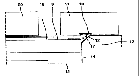
The distance between an optofibre 9 and an active surface 10
on an optochip 11 can be decreased by reducing a first part
of the distance, by "clipping off" a mirror 12 on a carrier
material 13 having a "vertical" wall 14; see Figure 2A. This
is achieved conveniently by sawing. The lower part of the
mirror 12 is completely sawn away with the same technique as
that used to separate microelectronic chips, wherein the
vertical wall 14 may commence in the bottom 15 of a groove
and terminate immediately beneath a fibre core 15 do the
optofibre 9. The distance between the fibre core and a
reflective point 17 on the mirror may be limited to about ZO
micrometers. The vertical wall 14 may also serve as an opto
fibre abutment surface therewith facilitating mounting of the
fibre.
The second part of the distance can be decreased by using a
fibre whose outer diameter is smaller than normal, meaning
that the diameter is smaller than 125 micrometers. Because
it must still be possible to handle the fibre, the outer
diameter or dimension may not be smaller than 60-80
micrometers. The total path length between the core 16 and
CA 02244067 2005-10-05
7
the active surface 10 will therefore be slightly longer
than about 70-90 micrometers.
With the intention of further decreasing said distance, the
fibre 9 has been beveled in the manner of a so-called D-
fibre; see Figure 2B. The D-fibre is, in principle, a
typical single mode fibre although with a D-shaped cross'
section, with the core 16 lying close to a fiat side 18 of
the modified optical fibre. This particular fibre shape is
obtained by sawing a perform, i.e. the "glass rode,
constituting the original fibre material along its length
at an appropriate distance from the core. The fibre
retains the proportions of the pre-form when laying the
fibre. This enables a fibre to be produced in which the
distance between the flat side and the core centre is very
short, less than 10 micrometers. Hy mounting a D-fibre in
a v-shaped groove 19 with the flat side 18 of the D-fibre
facing upwards, the total path length, fibre to optochip,
can be kept beneath 20 micrometers.
Something which is not evident from Figure lA-D is the
difficulty experienced in placing an optofibre in a V-
groove with the optofibre remaining in abutment with the
walls of the groove. The optofibre is most usually glued
in the v-groove. However, the glue tends to lift the fibre
out of position, with a negative effect on the desired
mounting precision. Consequently, the use of an auxiliary
means to hold the fibre in position during the gluing
process would be desirable. One such auxiliary means may
have the form of a cover means or lid 20 secured on top of
the carrier material, such as the silicon carrier 13, such
that the v-groove 19 and the cover means 20 together form a
space having triangular capillaries 21, where the optofibre
fits exactly and is therefore unable to change position
during the gluing
Amended Sheet
CA 02244067 2005-02-25
WO 97/27507 $ PCT/5897/00102
process; see Figure 2B_ Figure 2C illustrates from above the
fibre 9 fixed in position by the cover means 20 and coupled
to the optochip I1.
The cover means 2D may be provided conveniently by anodic
bonding. An anodic bond is effected by placing together a
substrate carrier and a cover means, which may be made of
silicon or transparent glass, heating the assembly and
applying an electric potential. Mobile ions produce a high
field strength across a joint, where the electrostatic forces
contribute towards creating durable bonds on an atomic scale.
The strength of the joint is comparable with a strong glue
joint. Bonding is preferably effected on a so-called wafer
level, whexeafter separate carriers can be sawn from the
1S wafer. The carrier/cover assembly is configured to enable
certain parts of the cover to be sawn away so as to provide a
suitable optochip mounting surface. The combination of
triangular capillaries 21 and D-fibre 9 is particularly
suitable, since it is otherwise difficult to ensure that the
D-fibre will be affixed with its flat side upwards, since the
D-fibre will only fit with the V-groove capillary when
positioned correctly.
The aforedescribed solutions provide an optically
microstructure which is accurately fixated, has a short
optical path length and is particularly suited for mounting
on light-emitting or light-detecting optochips mounted on
silicon carriers.