Note: Descriptions are shown in the official language in which they were submitted.
CA 02244507 1998-09-04
TITLE: MICROWAVE AND MILLIMETER WAVE FREQUENCY MULTIPLIER
FIELD OF INVENTION: Apparatus and method for multiplying the output
frequency of an oscillator, particularly in the microwave and
millimeter-wave frequency bands.
BACKGROUND:
Conventional frequency multipliers are constrL.cted with chains
of frequency doublers using diodes. Such multipliers require the
insertion of driving power amplifiers between doublers to compensate
for the conversion losses accompanied by frequency multiplication.
Although conversion gain is achieved by using transistors such
as FETs, interstage amplifiers have been needed in high frequency
ranges such as millimeter-wave frequencies where small-power devices
have been used in many cases [1]. Recently, a frequency multiplier
chain without driving amplifiers has been reported [2], [3].
However, this consists of cascaded frequency doubters where each
stage is designed independently so that input/output impedances at
each stage is matched to 50 ohm. As a consequence, stubs are
required for matching to 50 ohm in each input/output impedance
matching network. Since relatively small-power devices are used,
the power level is at most approximately 0 dBm. Employing medium-
power transistors for increasing the driving power level results in
the frequency bandwidth becoming narrower. This is because a
quarter-wavelength open-ended stub for suppressing the fundamental
frequency often lowers even further the input impedance, which is
originally relatively low, necessitating a larger transforming ratio
to 50 ohm.
References:
[1] H. Wang et al., "A W-band source module using MMIC's," IEEE
Trans. Microwave Theory Tech., Vol. MTT-43, No. 5, pp. 1010-1016,
May 1995.
[2] Ninomiya et al., "60-GHz transceiver for high speed wireless
LAN system", 1996 IEEE MTT-S Digest, pp. y171-1174.
CA 02244507 1998-09-04
[3] Hamada et al., "60 GHz phase locked oscillator using frequency
doubler", 1997 IEICE Spring Conf. C-2-45.
SUMMARY OF THE INVENTION
It is an object of the present invention to provide an apparatus
and a method for multiplying (by the power of 2) the output
frequency of an oscillator in low-frequency microwave bands.
It is another object of the invention to provide a highly
stable, low-phase-noise local frequency source in microwave and
millimeter-wave frequency bands.
Accordingly, the invention provides an impedance matching
network within a stage in a multistage frequency multiplier having
at least one stage, each stage having an input for receiving an
input signal of an input frequency and an output, said network
comprising:
means for suppressing the input frequency;
impedance stabilization means;
a transmission line having a capacitor, a first. end coupled to
the suppressing means, and a second end coupled to the stabilization
means, whereby matching is achieved by setting appropriate
parameters of the transmission line.
In another aspect, the invention provides a method for matching
impedance of a stage in a multistage frequency multiplier having at
least one stage, each stage having an inpur_ for receiving an input
signal of an input frequency and an output, comprising the steps of:
a) suppressing the input frequency;
b) inserting a transmission line within said stage;
c) setting said impedances by setting appropriate parameters of
said transmission line;
c) stabilizing said impedances.
One advantage of the present invention is a simplification of
the circuit topology because the stubs for impedance matching are
eliminated, resulting also in a reduction in the total size of the
circuits. Another advantage is that when cascading doublers using
medium power three-terminal devices, driving power levels can be
CA 02244507 1998-09-04
increased keeping the bandwidth from getting narrow, thereby
stabilizing the output power level required from a local oscillator.
The apparatus and method of the invention are of particular use
in high-speed, large-capacity communications systems and in
microwave and millimeter-wave radar.
DRAWINGS
Fig. 1 shows a conventional frequency multiplier consisting of
two frequency doubler stages;
Fig. 2 shows an interstage network in accordance with the
present invention;
Fig. 3 shows a three-stage frequency multiplier in accordance
with the invention;
Fig. 4 shows the measured fourth harmonic output power and the
conversion gain of a quadrupler in accordance with the invention;
Fig. 5 illustrates the suppression of unwanted harmonics; and
Fig. 6 illustrates eighth harmonic output power versus input
power for the three-stage multiplier of Fig. 2.
DETAILED DESCRIPTION
This invention, for the first time, introduces the concept of
interstage matching to multi-stage frequency multipliers, assuming
no need for driving amplifiers between doublers. The interstage
network consists of a quarter-wavelength (i~/4) open-ended stub 1 for
suppressing the input frequency signal, and a transmission line 2
including a DC block capacitor 3: A shunt resistor 4 on the gate 5
is used for stabilization when the input impedance of the next stage
doubler is negative. Impedance matching between devices is made by
selecting the appropriate characteristic impedance of the
transmission line 2 and its electric length. This configuration is
feasible with frequency doublers using (medium-) power transistors,
which can yield conversion gain at successive stages and maintain
the driving power levels high enough.
This apparatus is preferably used for multiplying the output
frequency of phase-locked loop oscillators in order to provide
CA 02244507 1998-09-04
highly-stable, low-phase-noise local frequency sources in microwave
and millimeter-wave frequency bands.
This apparatus can also be used for multiplying the output
frequency of voltage controlled oscillators in order- to provide
output signals from radar transmitters in microwave and millimeter-
wave frequency bands.
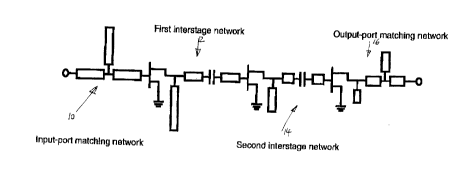
Figure 3 shows the configuration of a three-stage frequency
multiplier in accordance with the invention. This consists of the
input-port network 10 for the fundamental frequency matching, inter-
stage matching networks 12, 14 for the second and the fourth
harmonic signal, respectively, and the output-port network 16 for
the eighth harmonic matching. Pinchoff bias operation is adopted
for less DC power consumption, and also for keeping lower frequency
harmonics from being amplified. On the output side of each device
is placed a quarter wavelength open-ended stub 1 fo:r suppressing the
input frequency signal to each stage. On these conditions, (S11) of
each medium-power FET can be close to unity in the vicinity of the
input frequency, while (S22) of the preceding device is smaller
enough than unity. Leaving the magnitudes as they .are, the phase of
the reflective coefficients is conjugately matched :by selecting the
appropriate characteristic impedance of the interstage transmission
line 2, which includes a DC block capacitor, and its electric
length.
In a preferred embodiment, the apparatus includes microstrip
lines on 250-um thick Alumina substrates mounted on metallic
carriers. Medium power devices are Fujitsu FSX52X, commercially
available 600-~m MESFET, for the first-stage doubler, and GaAs-based
500 ~.m PHEMTs from Northrop-Grumann for the second and third stage.
This design is based on the measured small-signal S parameters.
Open-ended stubs are used for the input- and the output-port
matching networks 10, 16.
In this embodiment, the first- and the second-:stage doubling
circuits have only a fundamental frequency suppression stub on their
output port. During testing of the doubling circuits, a phase
shifter was placed between the two circuits, and the phase was
CA 02244507 1998-09-04
varied. The fourth harmonic power varied by 9 dB with a period of
180 degrees. The phase difference between the angles which give 1
dB less output power than the maximum level was 25 degrees. This
relatively insensitive feature is advantageous for cLesign.
The frequency quadrupler consisting of the inpur_ matching
network 10 for the fundamental frequency, and the first and the
second interstage matching networks 12, 14, in this embodiment a
quadrupler to 14.25 GHz, was tested. Measured fourth harmonic
output power and the conversion gain of this quadrupler is shown in
Fig. 4 as a function of input power. A maximum conversion gain of
13.8 dB is obtained for an input power of -1 dBm. The unwanted
harmonics were suppressed by less than -25 dB as shown in Fig. 5.
The combination of the output-port matching network 16 for the
eighth harmonic with this quadrupler constitutes the: three-stage
multiplier. Measured eighth harmonic output power versus input
power is shown in Fig. 6. The preferred multiplier shows a maximum
conversion gain of 6.1 dB for the input power of -3 dBm. The output
power of 4.3 dBm was obtained for 0 dBm input power.. The total DC
power consumption is 257 mW when the input power is 2 dBm.