Note: Descriptions are shown in the official language in which they were submitted.
CA 02245113 1998-08-14
CA9-98-026
ZERO POWER POWER-ON RESET BOOTSTRAPPING METHOD AND APPARATUS
FOR ULTRA LOW-POWER INTEGRATED CIRCUIT PACKAGING
Background of the Invention
Field of the Invention
This invention relates to a circuit for selecting internal integrated circuit
chip functions and
more particularly to a circuit which can select the functional operation of
the integrated
circuit chip without external pull-up resistors.
Description of Related Art
This invention enables the design of an integrated circuit chip having
multiple
configurations which may be selected without the use of external pull-up
resistors and
without the use of additional input/output pins in the integrated circuit
packaging.
Standardized packaging typically has a fixed number of input/output pins. For
instance an
8 pin package would typically have only a single power supply voltage pin
which would
likely have only limited space for bonding. However although there would
likely only be a
single ground pin there would be, conversely a substantial amount of space on
grounded
2o portions of the lead frame used in the package to tack terminal pads of the
integrated
circuit to ground as desired.
Bootstrapping resistors such as pull-up or pull-down resistors while being
useful solution
to the problem cause complications because of size limitations and power
consumption.
25 Both of these complications are undesirable because of the small size of
integrated
circuitry and because of the desirability of reducing power consumption to an
absolute
minimum required for battery power of the circuitry.
We have found that wire bond bootstrapping of an integrated circuit inside a
molded
CA 02245113 1998-08-14
CA9-98-026 2
package at the time of packaging can be used to enable or disable modes of
operation of
the integrated circuit.
Summay of the invention
To overcome the limitations in the prior art which require the use of an
external pull-up or
pull-down resistor and to minimize power consumption has will become apparent
upon
reading and understanding the present specification present invention
discloses a system
in which multiple configurations and integrated circuit chips operation may be
controlled
without external pull up or pull down resistors or additional lead frame pins.
One aspect of the invention provides low-power selector circuit contained
within the
integrated circuit chip being controlled for selecting between a plurality of
functions of the
integrated circuit chip comprising:
a gated pull up resistor for connection to a power supply and connected to an
input/output
terminal of the integrated circuit chip;
a sampling latch;
a power-on reset circuit;
the sampling latch being adapted on enablement by the power-on reset circuit
to sample
voltage on the input/output terminal of the integrated circuit chip on
powering up and output
2o a control signal to control functions of the chip, and; if the input/output
terminal has been
grounded to gate the pull-up resistor into an off state.
In another aspect of the invention the gated pull-up resistor is connected
between an
externally accessible input/output terminal pad of the integrated circuit chip
and the power
supply terminal pad to which power can be supplied to said chip. The sampling
latch has
a sampling input connected to the input/output terminal to sample the voltage
level at the
terminal and also has an output for producing 8 control signal directed to
control functions
of the chip. The power-on reset circuit is adapted to enable the latch on
power-up to
sample the voltage at the input/output terminal and latch that voltage to its
output to output
CA 02245113 1998-08-14
CA9-98-026
a control signal and, if the input voltage is low i.e. grounded to switch off
the gate of the
pull-up resistor so that power consumption will be minimized.
Preferably the gated pull up resistor consists of a gating circuit such as a
transistor in the
integrated circuit chip.
The sampling latch may consist of a latching flip-flop having an enabling
input connected
to the output of the power-on reset circuit and a latchable output for
producing the control
signal, and an inverted output, the output of the power-on reset circuit and
the inverted
output being connected to the inputs of an and gate, the output of which is
connected to
the control gate of the gating transistor for gating the current through the
resistor.
Brief Descriation of the Drawings
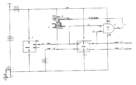
Figure 1 is a schematic circuit of a preferred embodiment of the invention;
Figure 2 is a diagram illustrating the behavior of the embodiment of Figure 1
including the power-on reset voltage of the circuit of the invention and the
power supply
voltage in relation to time for the case where the input pad PADIN of the
integrated circuit
chip is grounded:
Figure 3 is a diagram of a lead frame for an integrated circuit package
depicting
2o connections to terminal pads of an integrated circuits jet in which an
input/output terminal
pad of the chip has been grounded;
Figure 4 is a diagram of a lead frame for an integrated circuit package
depicting
connections to terminal pads of an integrated circuit chip in which can
input/output terminal
pad of the chip previously depicted in figure three has been left ungrounded.
Figure 5 is a diagram illustrating the behavior of the embodiment of Figure 1
including the power-on reset voltage of the circuit of the invention and the
power supply
voltage in relation to time for the case where the input pad PADIN of the
integrated circuit
chip is NOT grounded;
CA 02245113 1998-08-14
CA9-98-026
Detailed Description of the Invention
In the following description of the preferred embodiment of the invention
references made
to the coming drawings and in which is shown by way of illustration a specific
embodiment
in which the invention may be practiced. It will be well understood that other
embodiments
of the invention may be used without departing from the scope of the present
invention.
In the packaging of integrated circuit chip we usually only have access for
the construction
of wire bonds from input/output pads on the chip to module pins of the
packaging or to
some contact areas on the lead frame, typically a ground plane of the frame.
There is
typically more space available on the frame ground; and in addition, noise and
thermal
considerations essentially dictate that grounded lead frames be used.
If multiple modes of operation of the integrated circuit chip are needed but
extra module
or packaging pins are not available or would necessitate major design changes,
such as
~5 additional pins, which are typically undesirable in an industry that values
standardization
then another solution must be found.
It is not usually difficult to add additional input/output terminal pads to an
integrated circuit
chip for the purpose of mode selection, for instance, if the input/output
terminal pad is
2o grounded then operation mode one is selected; however, if the voltage level
of the
input/output terminal pad is high then operation mode two has been selected,
for instance.
To carry on example, at packaging we can wire bond an input/output terminal
pad to the
lead, the same frame ground to select mode one. This does not cause much
problem as
25 a digital input has been grounded. If, however, we choose to leave the
input/output
terminal pad ungrounded, and which case the pad will be floating there may be
a
significant problem as the terminal is floating and its state is unknown. It
is unacceptable
in digital technology to leave a digital input floating as will be well
recognized by those
skilled in the art.
CA 02245113 1998-08-14
CA9-98-026 5
Another alternative(not depicted in the drawings) which alleviates the
floating pad problem
is to use a pull-up resistor connected between the input/output pad and the
supply voltage
(Vdd) of the chip. If the input/output pad of the chip is grounded it will be
stable and mode
1 will have been selected. If , on the other hand, the pad is not grounded
then the pull-up
resistor will pull its voltage up to Vdd to select mode 2. Again this is
stable as the pad is
not floating. However, in this case there is a further problem. With the pad
grounded a
current, which we will call Idc, flows through the pull-up resistor. If we
want to reduce the
current flow, to reduce losses for battery operation, (taking into account
that a modern
design may use only 50 nA for a whole integrated circuit chip when in its
power saving
1o shutdown mode) we would attempt to use on-chip resistors to reduce the
current.
Unfortunately, at this time, economical on-chip resistors may have values of
about 100
Kohms. For a 3 volt supply this would result in an Idc current of 30
microamps. This is
unacceptable, being many orders of magnitude larger than the shutdown current
consumption of the entire chip.
We have found that one solution to this problem is the use of a gated pull-up
resistor
formed on an integrated circuit chip that is controlled by a latch that
samples the voltage
on the terminal input pad and shuts off the pull-up resistor if it detects a
low, i.e. a
grounded input terminal pad. When activated this would reduce the current Idc
through
2o the pull-up resistor to zero.
Referring to Figure 1 which shows one embodiment of the invention it may be
seen that
the circuit of the invention includes a gated pull-up resistor namely resistor
4 and FET
transistor gate 5 which is controlled through its gate 10 by the output 9 of
And gate 6 which
receives its input controls from Power-On Reset circuit 2 and the inverted Q
output 14 of
sense latch flip flop 3. The Power-On Reset circuit 2 enables sense latch 3
when the
voltage supplied to it by Vdd the supply voltage exceeds a threshold voltage
Vth on power-
up. Further details of Power-On Reset circuit 2 will not be given as there are
many
implementations familiar to those skilled in the art. The sense input 11 of
latch 3 as well
CA 02245113 1998-08-14
CA9-98-026
as one end of pull-up resistor 4 is connected to input/output terminal pad 1
of the
integrated circuit containing the circuit of the invention. This pad 1 may be
grounded by
ground 15, for example, by being wirebonded to the ground of the circuit
package lead
frame as discussed above as shown in Figure 3, or left ungrounded as shown in
Figure
4, in which case pull-up resistor 4 will cause the input 11 of latch 3 to be
pulled to the
supply voltage level Vdd. The output signal 7 from the latched output 13 of
latch 3 is used
to control the functions of other circuitry of the integrated circuit chip
(not shown) to obtain
the desired functions. For instance, output level 1 (high) on output 7 may
result in one
mode of operation and a level 0 will result in another. The output 13 will
hold whatever
state was present on pad 1 when the rising edge of the output of the power-on
reset circuit
2 exceeded a preset threshold voltage Vth as shown in Fig. 2. The output of
the power-on
reset circuit is held low by the circuit until the supply voltage Vdd to it
exceeds Vth.
Comparison of the final states of MODE and MODE- in Figure 2 and Figure 5
clearly
indicate the functionality of the circuit in the presence (Fig. 2) or absence
(Fig. 5) of a
~5 connection to ground.
The operation of the circuit of the invention and its advantages may be
appreciated from
the following description of its operation:
2o The power-on reset circuit is conveniently supplied by the same supply
voltage Vdd that
powers the integrated circuit chip.
As Vdd increases in voltage on power-up, but prior to reaching Vth, the output
9 of And
gate 6 is kept low, i.e.. 0 because the output (PON) of the power-on reset
circuit 2 is 0 as
25 shown in region A of Fig. 2. Under this circumstance the state of FET
transistor 5 is ON
and if terminal pad 1 of the chip is wirebonded to ground then current will
flow through
transistor 5 and pull up resistor 4 to ground through wirebond 15.
If on the other hand, the wirebond is not made then no current will flow
through pull up
CA 02245113 1998-08-14
CA9-98-026
resistor 4 and the voltage present at pad 1 will equal Vdd, the supply
voltage, i.e.. the pad
voltage is pulled up to the supply voltage Vdd. As we have still not crossed
the Vth
threshold the power-on reset voltage output from power-on reset circuit 2 is
still low.
At a later point in time during power-on , as shown in region B of the power-
on trace of Fig.
2 when the supply voltage Vdd has exceeded Vth, the threshold voltage, then
the output
(PON) of power-on reset circuit 2 will rapidly rise from 0 (low state) to 1
(high state), and
on that rising edge, sensing latch flip flop 3 will be enabled by the output
of power-on reset
2 at input 12, latching the state of pad 1 sensed at input 11 onto the output
13 of latch 3.
As the output of power-on reset circuit 2 is high the output of And gate 6
will depend on
the inverse 14 of the latched output 13 of latch 3.
If the wirebond 15 is made to ground, (as illustrated in Fig. 4. which shows
pad 1
connected to the ground plane of a lead frame 40 during the course of
manufacturing, prior
~5 to encapsulation and lead severance) then output 13 of latch 3 will be 0
and consequently
the inverse output 14 will be 1, thus And gate 6 will output a level 1 output
(high) causing
gate 5 to turn off (note the inverting behavior of gate 5). This will result
in the current
through pull up resistor 4 being reduced to zero after the state of pad 1 has
been sensed,
with power savings resulting. Figure 2 illustrates the response at several
points in the
2o circuit as the power supply voltage Vdd is applied, eg. at turn on.
On the other hand, if wirebond 15 is not present, i.e. if the pad was not
grounded, (as
shown in Fig. 3, which shows an ungrounded pad 1 of a chip contained on a lead
frame
assembly prior to encapsulation and lead severance), then on power-up the when
the
25 supply voltage Vdd exceeds Vth the voltage of pad 1 will be pulled up to
Vdd, i.e.. state 1.
The output 13 of latch 3 will be latched high to produce a high output control
signal 7 for
use by other circuitry of the chip as described. The inverse output 14 of
latch 3 will be set
to 0 and the output of And gate 6 will be 0, thus FET transistor 5 will stay
on. This is of
little consequence as this situation can occur only if pad 1 was not grounded.
Therefore
CA 02245113 1998-08-14
CA9-98-026
resistor 4 will not be conducting current as the voltage of pad 1 will have
been pulled up
to supply voltage Vdd. Figure 5 illustrates the response at several points in
the circuit as
the power supply voltage Vdd is applied, eg. at turn on.
As will be realized from this description, the circuit of the invention
effects a sampling of
the voltage of a pad of the integrated circuit chip to determine whether or
not it has been
grounded and uses this information to control the functions of other circuitry
on the chip.
It accomplishes this with very little power consumption, unlike prior art
devices, and
requires no external resistive components.
The present invention is not limited to the specifically disclosed
embodiments, and
variations and modifications may be made without departing from the scope of
the present
invention.