Note: Descriptions are shown in the official language in which they were submitted.
CA 02245303 1998-08-19
-1-
METHOD AND APPARATUS FOR
AUTOMATIC COMPENSATION OF FIRST-ORDER
POLARIZATION MODE DISPERSION (PMD)
FIELD OF THE INVENTION:
The invention relates to optical transmission systems and more
particularly relates to dealing with so-called polarization mode dispersion in
such systems.
BACKGROUND OF THE INVENTION:
Polarization Mode Dispersion (PMD) occurs in an optical fiber as a
result of a small residual birefringence that is introduced in the fiber core
by asymmetric internal stress or strain as well as random polarization
coupling due to external forces acting upon the fiber. Consequently, PMD
may severely impair the transmission of a signal in an optical fiber
network.
It is well-known that PMD affects differently certain polarization
components of an optical signal propagating through a optical fiber
transmission line, such that differential time delays occur among the
components as they travel through the fiber. These differential time delays
may range from about 0.lps/(km)1~2 for low-PMD optical fibers of modern
manufacture to several ps/(km)1~2 for single-mode optical fibers of older
manufacture. Disadvantageously, the differential time delay that may
result over a "long-distance" fiber-optic link, for example, a 100 km
terrestrial transmission system employing single-mode fiber, due to such
differential delays may be more than 20 ps, or more than 10 ps for an
transoceanic link employing modern low-PMD optical fiber.
CA 02245303 1998-08-19
-2-
The large time delays that occur between different polarization
components of an optical signal may cause significant broadening of the
optical pulses propagating through an optical link. This is especially true
in modern digital lightwave systems which operate at bit rates of at least 10
Gbps per transmitted-wavelength-channel. In fact, the broadening of a
pulse by a differential time delay of, e.g., about 20 ps, in a high-bit rate
system may cause a partial closure of the "eye diagram" of the received
electrical signal by about 0.5 dB, which will significantly distort a received
signal.
It is well-known, however, that the differential time delay that might
occur in a particular transmission fiber is not constant over time, but may
vary over time as the physical environment, e.g., temperature, pressure,
etc., of the fiber changes. Thus, the statistics of time-dependent
differential
time delay caused by PMD in optical fiber usually follows a Maxwellian
distribution, and, therefore, at any point in time, may be substantially
lower to several times higher than its average (or mean) value.
(Note that in some older high-PMD optical transmission fibers a
differential time delay of up to, e.g., 100 ps, is theoretically possible. A
time
delay of that order may cause, for example, complete fading in the electrical
signal, as reported in, for example, the article entitled "Polarization
Effects
on BER Degradation at 10 Gb/s in IM-DD 1520 km optical Amplifier
System" by Y. Namihira et al, and published in Electronic Letters, Vol. 29,
No. 18, p. 1654, 1993.)
Prior methods of dealing with signal impairments due to PMD in an
optical fiber include, for example; (a) electrical equalization of the signal
distortion caused by PMD, as discussed in the article entitled "Experimental
Equalization of Polarization Dispersion", by M. A. Santoro and J. H.
CA 02245303 1998-08-19
-3-
Winters, and published in IEEE Photonic Technology Letters, Vol. 2, No. 8,
p. 591, 1990; and (b) electrical compensation of the differential time delay
in
the received electrical signals, as discussed in the article entitled
"Polarization Mode Dispersion Compensation by Phase Diversity Detection",
by B. W. Hakki and published in Photonic Technology Letters, Vol. 9, No. 1,
p. 121, 1997. Such prior methods also include (a) optical compensation of
the differential time delay before converting the optical signals into
electrical signals, as discussed in the article entitled "Polarization-Mode-
Dispersion Equalization Experiment Using a Variable Equalizing Optical
Circuit Controlled by a Pulse-Waveform-Comparison Algorithm", by T.
Ozeki et al, and published in the Technical Digest Conference on Optical
Fiber Communication 1994 (OSA), p. 62; and (b) other forms of
compensation as discussed in, for example, the article entitled "Automatic
Compensation Technique for Timewise Fluctuating Polarization Mode
Dispersion in In-Line Amplifier Systems", by T. Takahashi et al., and
published in Electronic Letters Vol. 30, No. 4, p. 348, 1994.
Disadvantageously, such electrical equalization schemes can only
compensate for a relatively small differential time delay. They also require
expensive high-speed electronics. Moreover, prior art optical compensators
in general cannot automatically adapt their respective compensation
schemes to handle a varying differential time delay in an optical signal
traveling in a fiber that is being affected by a fluctuating-random PMD. For
example, the optical compensation described in the Takahashi et al. article
generates a fixed optical time delay to compensate for the distortion caused
by PMD in a transmission fiber. Therefore, such a scheme is limited to
dealing with a relatively small range of differential time delays. As another
example, although the compensation scheme described in the T. Ozeki et al.
article is capable of generating a variable, adaptive differential time delay,
CA 02245303 2002-O1-18
-4-
it requires expensive high-speed electronics to analyze the shape of received
waveforms and derive an error signal that may be used to drive the
compensation process toward the desired differential time delay.
SUMMARY OF THE INVENTION:
We deal with the foregoing problems and advance the relevant by
providing apparatus which automatically adapts to the level of first-order
polarization mode dispersion that may be present in an optical signal received
from an optical transmission line. Specifically, we use a variable optical
birefringence element which, responsive to receipt of the optical signal,
generates a differential optical time delay between at least two selectable
mutually orthogonal polarization states. An optical signal analyzer coupled to
the output of the variable birefringence element, in turn, generates a control
signal proportional to the total differential optical time delay that is
present in
an optical signal appearing at the output of the variable birefringence
element.
The control signal is supplied to the birefringence element to control the
amount
of differential time delay that is generated to control which orthogonal
polarization states are selected.
In this way, we automatically and adaptively generate a differential time
delay that substantially equals the differential time delay that occurs in the
transmission optical fiber, but of opposite sign, and, therefore, cancels out
the
undesired delay.
In accordance with one aspect of the present invention there is provided a
compensator for compensating for the effects of polarization mode dispersion
occurring in an optical transmission fiber having principal states of
polarization,
the compensator comprising a polarization transformation element operative for
reorienting the polarization of particular components of an optical signal
received over the optical transmission fiber, apparatus operative for dividing
a
CA 02245303 2002-O1-18
-4a-
signal supplied at an output of the polarization transformation element into a
predetermined number of signals each having a polarization state oriented
orthogonally to a respective one of the two principal states of polarization
and
for delaying each such divided signal a variable amount of time; and an
analyzer operative for analyzing a signal outputted by the apparatus for
delaying
and generating a distortion indicator having a level indicative of a level of
distortion in the analyzed signal and supplying the distortion indicator to
the
polarization transformation element and said apparatus, and wherein said
polarization transformation element and said apparatus, responsive to a change
in the level of the distortion indicator respectively changing, until the
level of
the distortion indicator reaches a predetermined state, the orientation of
each
said polarization state and said variable amount of time.
In accordance with another aspect of the present invention there is
provided an optical transmission system comprising an optical transmitter that
transmits an optical signal to an optical receiver via an optical fiber
transmission
line, a receiver that receives the optical signal from the transmission line
and
generates a differential time delay between selectable mutually orthogonal
polarization states of components of the received optical signal, said
receiver
including an analyzer operative for generating a control signal having a value
proportional to the value of the differential time delay, said receiver
changing
the value of the differential time delay and selection of the two orthogonal
polarization states as a function of the current value of the control signal
and
doing so until the value of the control reaches a predetermined level.
These and other aspects of our invention are set forth in the following
detailed description, corresponding drawings and ensuing claims.
BRIEF DESCRIPTION OF THE DRAWINGS:
CA 02245303 1998-08-19
- 5-
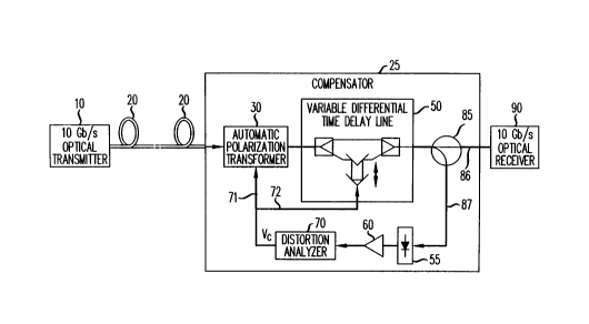
FIG. 1 illustrates in block diagram form an illustrative system in
which the principles of the invention may be practiced;
FIG. 2 is a block diagram of the distortion analyzer of FIG. 1;
FIG. 3 illustrates in graphical form a simulation of the feedback
signal versus the total differential group delay for filtered, unfiltered and
weighted 10 Gb/s pseudo-random sequences;
FIG. 4 illustrates in block diagram form another illustrative system
in which the principles of the invention may be practiced;
FIG. 5 illustrates in graphical form a plot of the total differential
group delay against the polarization transformation angle associated with a
polarization transformer of FIG. 4;
FIG. 6 is a block diagram of an illustrative embodiment of an
integrated circuit version of the differential delay line of FIG. 1; and
FIG. 7 is alternative embodiment of the system of FIG. 1 in which a
signal scrambler is employed at the transmitter of an optical signal.
FIG. 8 illustrates a distortion analyzer that may be used to derive a
feedback signal for the inventive PMD compensators in FIGs. 1 and 4.
DETAILED DESCRIPTION:
Polarization Mode Dispersion (PMD) occurs in single-mode fibers as a
result of residual birefringence in the fiber core and coupling of random
polarization at various points along the fiber. The polarization
transformation that occurs in the fiber may be modeled using a simple
unitary 2x2 Jones matrix, U, as shown by following expression;
CA 02245303 1998-08-19
- 6-
_ ul(to) u2(w)1 (1)
IT(c~) C-u= (r~) u1 (w)
2
where u~ and u2 in general are complex functions which depend on the
frequency, c~, of the optical signal and other physical parameters that
influence the mode coupling in the fiber.
It is well-known that for any optical frequency, c~ _ ~o, there exists
two orthogonal states of polarization commonly referred to as the Principal
States of Polarization (PSP). An optical signal propagating through a fiber
does not experience any significant amount of differential time delay if it is
polarized at one of the two PSP. Thus, at any optical frequency, w = coo, the
matrix U may be "diagonalized" in the following way
U(~) = w(~o) . D(~) . V(~o)-1
vll vlz and W = wll w12 (3)
where: V
Cw21 w2
Cv
21
are unitary matrices and;
0
is a diagonal matrix.
0 a
v1 l = w12
The Jones vectors; ~jr,;"= ~ , Y~2~n
vz vz
CA 02245303 1998-08-19
_ 7-
and yr = w"~ yr =Cwl2J correspond to the
w zaur wzz
a
input and output principal states of polarization, respectively. Also, the
frequency dependency in matrix D can be approximated to a first order in
(c~ - coo), at least over a sufficiently small frequency interval 0~ around
coo,
as follows:
>(2f12)(~-~o)
D(co) I7(o°) ~ a .I(2fl2)(w-«o) (6)
0 a
2 2
d d
where 'Cf = 2 u1 + u2 is the Differential Group Delay (DGD)
d~ d~
that causes the aforementioned differential time delay in optical signals
that are not launched in one of the two Principal States of Polarization
to (PSP).
It can thus be appreciated from the above equations that a
differential time delay, ~f, occurs between the two PSP of the fiber. The
differential time delay which an optical signal experiences as a result of
propagating through an optical fiber may, therefore, be compensated for by
introducing an opposite but equal amount of differential time delay, 'L~ _ -
'Lf,
at the output of the fiber, in accordance with an aspect of the invention.
This may be readily done using an optical element having the following
polarization dependent transfer function:
-J(~-~o) Z~/2
Ucomp = a J(~-~o)Z~/2 ' D-1(c°o) ~ W-1(°~0)
CA 02245303 2002-O1-18
_8_
where D and W are the matrices shown in equation (3). The matrix Ucomp
describes first order PMD (i.e., uniform birefringence) at an arbitrary
orientation.
As mentioned above, PMD in a fiber may change with changes in time
and optical frequency. This change in PMD may be dealt with, in accordance
with another aspect of the invention, by varying the amount and orientation of
the birefringence in the inventive compensator to adaptively compensate for
the
DGD in the fiber. An adaptive, variable-birefringence compensator may be
readily realized by disposing a polarization transformer 30, for example, the
polarization transformer described in U.S. Patent No. 5,212,743 issued May 18,
1993 to F. Heismann, in series with an element 50 that generates variable
linear
birefringence (such as, for example, the polarization mode dispersion
emulator,
model PE3 available from JDS Fitel Inc.), as shown in Fig. 1. Such
birefringence may be so generated, in accordance with another aspect of the
invention, by splitting the signal at the output of the polarization
transformer
into two orthogonal linear polarization states corresponding to the two PSP of
the fiber, and delaying each of the two polarization states by a variable
amount
of time, i~, using a respective delay line 50 as shown in FIG. 1. In fact, if
the
polarization transformation that occurs in polarization transformer 30 and the
time delay in the variable differential time delay line 50 are properly
adjusted
such that polarization transformer 30 generates the polarization
transformation
described by the matrix W'1 expressed by equation (7) and such that variable
differential time delay line 50 generates the differential time delay i~ shown
in
(7), then a signal outputted by the compensator 25 will be free of the
distortions
caused by differential time delays occurring in transmission fiber 20.
CA 02245303 1998-08-19
- 9-
Note that an optical element (such as, for example, a combination of
properly aligned birefringent fibers connected in series) that generates
variable frequency dependent birefringence may be used in a similar
manner to compensate for signal distortions due to higher-order PMD.
However, a polarization transformer in series with a variable birefringence
compensator alone would not automatically adapt by itself to changes in the
PMD of the fiber. Such automatic adaptation may be achieved, in accord
with another aspect of the invention, by providing a feedback signal that
controls the polarization transformation occurring in the polarization
transformer 30 (i.e., the orientation of the variable birefringence) as well
as
the differential time delay in the variable differential time. delay line 50
(i.e., the amount of linear birefringence). The desired feedback signal may
be generated at the output of compensator 25 by monitoring the amount of
distortion that is due to the differential time delay present in an optical
signal after it has traveled through compensator 25.
We have recognized that, that in accordance with another aspect of
the invention, only one feedback signal is needed to simultaneously adjust
the polarization transformation and adjust the differential delay, i~, to
achieve minimal distortion in the signal that compensator 25 outputs to
optical receiver 90 via conventional signal tap 85, as is shown in FIG. 1 and
as will be discussed below.
Specifically, a portion of the signal that compensator 25 outputs is
supplied via optical tap 85 to path 87 extending to high-speed photodetector
55, which may be, for example the Hewlett Packard Co., model 11982
Wideband Lightwave Converter having an electrical bandwidth that is at
least equal to the information bandwidth of the modulated optical signal
transmitted by optical transmitter 10. The remainder of the signal is
supplied to path 86 extending to receiver 90. Photodetector 55 converts the
CA 02245303 1998-08-19
- 10-
high-speed digital information signal modulated onto an optical carrier
signal into an electrical signal. The electrical signal is then amplified by
conventional amplifier 60 and coupled to electrical distortion analyzer 70
which measures the distortion in the amplified photocurrent and converts
the amplified result into a voltage, Vf, that is proportional to the
distortion.
For example, voltage Vc reaches a maximum value when the optical signal is
free of distortion due to first order PMD, i.e., when the combined
differential time delay of optical fiber 20 and compensator 25 is
substantially equal to zero. The combined DGD, itot~, introduced in fiber 20
and compensator 25 may be expressed as follows:
icotai = .~ Z f + Z~ + 2 Zf 2~ cos(29) (8)
where if is the DGD in fiber 20, ~~ is the DGD in compensator 25 and 2 eis
the angle between the so-called Stokes vectors corresponding to the PSP of
fiber 20 and PSP of compensator 25, which is controlled directly by
polarization transformer 30.
It is apparent from equation (8) that the total differential time delay,
ztot~, is at a minimum value of ~ if - ~~~ when 2 Bis adjusted to a value of
~~,
i.e., when the so-called slow and fast PSP of fiber 20 are respectively
aligned parallel to the so-called fast and slow PSP of compensator 25. Thus,
the adjustment of the angle 9may be achieved by adjusting polarization
transformer 30 in response to the value of the feedback voltage, Vf,
supplied via feedback path 71 such that Veis driven to a relative maximum
value.
Also, the differential time delay, i~, in compensator 25 may be
adjusted in response to the value of feedback voltage, Ve, such that i~ is
CA 02245303 1998-08-19
-11-
substantially equal to the DGD, ~r, in fiber 20, thereby resulting in a ~c~c~
of
zero. At that point, Vf would be at a maximum value. Thus, if the
orientation and amount of differential time delay generated by polarization
transformer 30 and variable differential time delay line 50 axe adjusted in
the foregoing manner, then the level of distortion in the optical signal that
PMD compensator 25 outputs is minimal. Moreover, if either the orientation
or the level of DGD in compensator 25 deviates appreciably from the desired
values (i.e., 28 = -1~ and i~ _ ~f), then the signal that compensator 25
outputs will be distorted due to the resulting non-zero differential time
delay, ~totei .
It is well-known that the differential time delay, itot$i, between two
orthogonal polarization components in an optical signal modulated with a
high-speed information signal may cause, within an electrical frequency
band centered around a frequency of f = l/2i~tai, a partial or complete
fading in the detected electrical signal at the receiver. It was specifically
determined that after it has been detected by an optical photodetector, the
frequency response of an amplitude-modulated optical signal that has
experienced differential time delay i~t~ in an optical transmission line may
be described as follows:
S(~ _ 'V1-4Y(1-Y)sin2(~ztomf)
where f is the detected electrical frequency, 'y and (1-y) are the fractions
of
the optical power transmitted in the fast and slow PSP of the fiber, and the
function S describes a reduction in the photocurrent generated by
photodetector 55, with 0 <_ S <_ 1. Note that S(f) is equal to 1 if the
optical
CA 02245303 1998-08-19
- 12-
signal experiences no PMD in the transmission line (i.e., if zcotei = 0) and
that S(f) reduces to zero at f = (2i~t~)n if y = 0.5, i.e., if ic~tai ~ 0 and
the
optical signal has the same power level in each PSP. S(fj is thus a unique
measure of the distortion in the optical signal due to the total DGD in the
transmission fiber and the compensator.
If the DGD is limited to values below a maximum value, im$X, then
the distortion in the optical signal may be quantified by simply measuring
the amplitude of the received electrical signal of a particular frequency f <_
1/(2imaX). The amplitude of this signal may then be used as a feedback
signal to automatically adjust the orientation and level of DGD that is
generated in PMD compensator 25, such that the feedback signal is
maximized.
The above requirement set for the total DGD that may be inserted in .
a transmission system, ic~t~ <_ zmaR, may limit the amount of DGD that may
be compensated for in an optical transmission fiber, if, as itotai <_ 2~e. For
example, if in a 10 Gbps digital transmission system, the amplitude of the
received electrical signal is measured at 5 GHz, then if should always be
smaller that 50 ps. Otherwise, the feedback signal that is generated as a
function of the amplitude of the 5 GHz component may be ambiguous in the
sense that it is difficult to determine by which amount and direction the
polarization transformation, W-1, and the differential time delay, i~, need to
adjusted to obtain a i~c~ = 0, which may occur, for example, when the
amplitude of the feedback signal is the same for two different values of z~t~,
which may result in generating faulty adjustments in the orientation and
level of the differential time delay in PMD compensator 25.
CA 02245303 1998-08-19
13-
We have recognized, however, that an "unambiguous" feedback signal
(i.e., a signal that is a unique measure of Tc~t~) may be generated , without
limiting the level of compensation that may be applied to DGD, by
measuring the amplitude of a plurality of frequency components contained
in the optical information signal propagating through an optical fiber. An
illustrative embodiment of an inventive compensator which analyzes the
amplitudes of substantially the entire received frequency spectrum using a
broadband electrical power detector is shown in FIG. 2. The broadband
electrical power detector 95, which may be, for example, model 8474 diode
detector available from the Hewlett Packard Co., more particularly,
converts such amplitudes into a single feedback voltage, Vf, that is
proportional to the integral of the amplitudes (power levels) of
substantially the entire high-frequency electrical spectrum. (It is noted that
it is not necessary to include the DC component of the photocurrent in the
generation of the feedback voltage, since this component is usually not
affected by first order PMD.)
For the illustrative embodiment of FIG. 2, the feedback voltage, Vf,
generated by the distortion analyzer 70 (FIGS. 1 and 2) may be expressed as
follows:
fmax
Vf = const. ~ ,~ ld ( f )dj ~9)
f min
where ia(fj is the amplified version of the photocurrent that photodetector 55
supplies to amplifier 60, fmin and fmax are respectively the lowest and
highest
frequencies of the above-mentioned spectrum, in which, preferably, fmin <
f~n~k/100, where f~u~k is the clock frequency of the received digital
information, and fmax > f~u~k. For example, to compensate for a DGD of up to
CA 02245303 1998-08-19
- 14-
120 ps in a 10 Gbps transmission system, we found that a fmin of ~ 100 MHz
and a fmax of ~ 15 GHz to be sufficient for deriving a feedback voltage, Vf,
having a unique value. To obtain an "unambiguous" feedback signal, it may
be necessary to either filter or apply a weighting scheme to the electrical
spectrum possibly before or during the aforementioned integration process,
based on the spectral components contained in the digital information
signal modulated onto the optical signal. In that instance, the output of
amplifier 60 is passed through electrical filter 65 before it is detected by
power detector 95. This is graphically illustrated in FIG. 3 which shows a
graph of the feedback voltage that is obtained by integrating the entire
high-frequency spectrum of both unfiltered and filtered 10 Gbps digital
information signals, carrying a random or pseudo-random bit sequence
(PRBS), versus the total DGD, itot~, experienced by a respective optical
signal. Curve 310 shows that the feedback signal derived from an
unfiltered optical signal carrying PRBS exhibits secondary maxima at
values of i~t~ above about 180 ps, besides the desired absolute maximum at
itorai = 0.
Curve 330 of FIG. 3 also shows that appropriate filtering, or
weighting, represented by curve 320, of such frequency components
removes the undesired secondary maxima and, thus, provides an
''unambiguous" feedback signal that may be supplied to polarization
transformer 30 and adjustable delay line 50 to provide the desired level of
differential time delay in the desired polarization components of the
received optical signal. The polarization angle, 8, in polarization
transformer 30 and differential time delay, ~~, in delay line 50 may be
adjusted alternately until the level of the feedback signal, Vf, reaches a
maximum using a simple maximum search algorithm, such as the
algorithm disclosed in the aforementioned U. S. Patent No. 5,212,743. More
CA 02245303 1998-08-19
- 15-
specifically, the differential time delay in the delay line is continuously
dithered around its current value to determine the absolute maximum value
of the feedback voltage, Vf. Each time i~ is set to a different value, the
polarization angle, 8, is adjusted by the polarization transformer until the
level of the feedback signal, Vf, supplied by distortion analyzer 70 reaches a
maximum for that setting. This procedure is repeated for each value of
differential time delay, z~, until Vf reaches an absolute maximum value,
where the distortion due to first-order PMD in the received optical signal is
minimized.
(Note that Fig. 8 illustrates a distortion analyzer that may be used to
derive an "unambiguous" signal corresponding to curve 320.)
A second illustrative embodiment of our invention is shown in FIG. 4,
and includes a source of optical signals 410, optical transmission fiber 420,
and variable DGD compensator 425 formed from two sections each
respectively comprising first and second automatic polarization transformer
430 and 440 and first and second high birefringence, single-mode (HBF)
fiber 435 and 445 as shown. Fiber 435 (445) may be, for example, the
SM.15-P-8/125 fiber having a DGD of about 1.4 ps/m and available from the
Fujikura Company (Japan). The sections generate a differential time delay
of m and i2, respectively, between the light signals polarized along the slow
and fast optical axes of the respective section. The output HBF 445 is
coupled to an optional tap 485 connected to optical receiver 490. A portion
of the optical signal is fed via tap 485 to high speed photodetector 455.
Similarly, the electrical output of photodetector 455 is supplied to amplifier
460 and the amplifiied result is then supplied to distortion analyzer 470
comprising electrical filter 465 and broadband electrical power detector 495,
CA 02245303 1998-08-19
- 16-
which generates a feedback signal that is supplied to polarization
transformer 430 and polarization transformer 440.
Polarization transformer 440 in response to the feedback signal
rotates the state of polarization of the optical signal between HBF 435 and
HBF 445 such that transformer 440 effectively varies the angle, 6~, between
the fast axis of HBF 435 and the fast axis of HBF 445. The resulting
differential time delay, ~~, provided by the cascading of HBF 435 and 445
may be described by the following expression:
z~ _ .~ 2i + Zz + 2 2, 2zcos(28z ) (10)
which shows that the differential time delay generated by compensator 425
is continuously variable between a minimal value of ~ m - i~ and a maximal
value of (m + ~2).
Note that by choosing z2 of HBF 445 to be substantially equal to ~~ of
HBF 435 , the differential time delay i~ may be varied between 0 and 2~~ by
varying the polarization transformation in polarization transformer 440.
Also note that polarization transformer 430 operates similar to polarization
transformer 30 of FIG. l, since it is used to align the output PSP of the
transmission fiber parallel to the input PSP-of the variable birefringence
compensator formed by HBF 435, polarization transformer 440 and HBF
445 by varying the value of 8 in polarization transformer 430 such that the
feedback signal reaches a maximum. Transformer 440 then adjusts the
value of 8~ until i~ = ie. An example of that type of an adjustment is shown
in FIG. 5 in which the total DGD, itotai, is plotted against 8 and 0~. The
adjustment assumes that the fiber DGD is it = 70 ps, and that the
CA 02245303 1998-08-19
19-
differential delay in the HBF 435 and HBF 445 are respectively ~~ = 50 ps
and iz = 40 ps. It is seen from FIG. 5 that i~t~is approximately zero when
the value of 8 is ~/2 radians(which means that the slow PSP of transmission
fiber 420 is aligned parallel to the fast PSP of compensator 425) and when
the value 6~ is approximately 0.68 radians (alternatively 2.46 radians).
The system of FIG. 4 also automatically adapts the level of
compensation that it generates to a first-order P1VID if polarization
transformers 430 and 440 are controlled by a feedback signal that varies
proportional to the level of distortion in the optical signal that compensator
425 outputs to tap 485.
As described above, the feedback paths respectively shown in FIGS. 1
and 4 include similar elements. However, the possible range of differential
time delay that the system of FIG. 4 can compensate is limited by the total
bandwidth of the optical signal, i.e., the high-speed information signal that
is modulated onto the optical signal. Specifically, for the case where i2=z~,
the frequency-dependent polarization transformation in compensator 425
may be described by the following unitary matrix:
cosC ~c~ ,- sinC ec
Ucomp(GJ)= X
sinC ~c ~ , cos. ec
CA 02245303 1998-08-19
- 18-
I '~ 2 2 zl~~ +jsin(2ec)sin2~zle~~
j(1- jcosBc ~si~zl~m~~+ jcos ec sin 2 2
L
, . 2 zl~~ z Aro
-j[1+ jcos9c ~sin(zl~~)]- jcos2 Bc sin2C 1
j si~26 ~ sin
c 2
(11)
cos~e°~, sin~e°
2 2 x W(8)
- sing 8' J, co~ ~'
where ~co = ~ -~o, and W(8) is the polarization transformation in
polarization transformer 430. It is seen from equation (11) that for
i~=2m ~ cos8~ and to a first order in 0~, U~omP(c~) has the same desired form
of Eq. (7). However, the off diagonal terms in the second matrix on the
right side of Eq. (11) show that for laxge values of i~0~, a significant
amount of light is cross coupled between the PSP of the compensator.
Specifically, at 6~=~/4 radians and iWt~=~c radians, the light from either one
of the input PSP is completely coupled to the orthogonal output PSP.
Thus, if the total bandwidth of the optical signal is large compared
with either 1/m or lft2, then compensator 425 would not be capable of
simultaneously generating the desired differential time delay for all
frequency components of the optical signal to offset the effects of first-
order
PMD in the transmission fiber.
However, we have shown experimentally that for an amplitude-
modulated optical signal carrying a pseudorandom 10 Gbps digital signal, a
differential time delay of i~ = i~ = 50ps generated by compensator 425 still
CA 02245303 1998-08-19
19-
allowed for an adaptive PMD compensation with acceptable low levels of
second-order PMD distortion
Note that compensator 425 may be readily arranged to generate a
differential time delay greater than ~~ = m + i2 = 100 ps by merely adding
additional sections, as needed, in which, as mentioned above, each such
additional section comprises a polarization transformer and HBF with
differential time delays of ~s = 50 ps, i4 = 50 ps, and so on. Such a
compensator is also capable of compensating for the effects of second-order
PMD in addition to first-order DGD.
A broad block diagram of another illustrative embodiment of an
adjustable differential delay line operative for compensating for variable
first-order PMD is shown in FIG. 5. Similarly, as shown in FIG. 1, the
compensator system of FIG. 5 includes an element 540 at the input to split
(separate) the polarization of an incoming optical signal and an element 541
at the output to recombine the transformed PSP of the transmission fiber.
A variable time delay associated with one of the PSP is generated by a
number of asymmetric, waveguide Mach-Zehnder interferometers 530
through 532 connected in series via adjustable directional couplers 560
through 563, respectively. The directional couplers may be controlled in a
conventional manner to direct the optical signal either through the short or
long leg of the Mach-Zehnder interferometers 530 through 532, thereby
introducing a variable delay between 0 (zero) and i; = OL;~n/c; where ~Lc~n is
the optical path difference in the i-th interferometer and c is the speed of
light. It is thus possible to generate any desired differential time delay
between 0 (zero) and i~meX = (2n - 1) ~OL;n/c in discrete steps of ~i~ =
OLm/c.
To obtain an uninterrupted flow of the signal through the
interferometers while the delay i~ is being changed from one value to
CA 02245303 1998-08-19
-20-
another, the relative optical phases in each of the interferometers need to be
changed for constructive in-phase interference of the two optical signals
which emerge from the two arms of each Mach-Zehnder interferometer and
then enter the succeeding directional coupler. Therefore, it may be
necessary to include a variable phase shifter, e.g., a respective one of the
phase shifters 570 through 572, in each of the Mach-Zehnder
interferometer.
A controllable waveguide delay line based on the foregoing principles
may be readily constructed on a number of different electrooptic substrates,
such as, for example, lithium niobate and semiconductor materials as well
as other optical materials using, for example, thermo-optic or acousto-optic
effects to control the directional couplers 560 through 563 and phase
shifters 570 through 572.
It is noted that, for the PMD compensators shown in FIGS. 1 and 4, a
very low level of distortion might occur in the signal that the transmission
fiber outputs if most of the signal that is transmitted in one of the PSP of
the fiber, i.e., if y or (1- y) is small. Also S(f) would be close to 1, even
if a
large value of ~c is present in the transmission fiber. In that event, ~~ in
the
compensator would have some arbitrary value. Further, the level of
distortion in the optical signal might become suddenly large if the state of
polarization of the optical signal changes rapidly at some point along the
fiber, thereby requiring rapid adjustment of the values of 8 and z~ in the
PMD compensator.
The sudden adjustment of ~~ may be avoided by rapidly scanning the
input state of polarization to the transmission fiber over a large number of
different polarization states, such that, for example, averaged over time, all
possible polarization states are excited with equal probability. Then,
CA 02245303 2002-O1-18
-21-
approximately one-half on the input signal, on average, would be in one of
the PSP of the transmission fiber and the other one-half would in the other
PSP, i.e., on average '~ = 0.5 = 1-'~ . Consequently, a sufficient level of
distortion is consistently present in the optical signal supplied to the PMD
compensator to ensure that i~ is adjusted properly independent of changes
in polarization in the corresponding fiber.
To ensure that the feedback circuit in the PMD compensator remains
stable, the aforementioned scanning of the input polarization state to the
transmission fiber has to be performed much faster than the response time
of the polarization transformer that serves as the input to the PMD
compensator. One example capable of performing such scanning is the
electro-optic polarization scrambler disclosed in U. S. Patent No. 5,359,678
issued October 25, 1994 to F. Heismann et al.
FIG. 7 shows an illustrative embodiment of the invention that uses a
fast-electro-optic polarization scrambler 15 at the input of the transmission
fiber. Scrambler 15 may be modulated with an arbitrary voltage, e.g., a
sinusoidal or sawtooth voltage, as long as the average degree of polarization
of the light signal that scrambler 15 outputs is substantially equal to zero.
The foregoing is merely illustrative of the principles of the invention.
Those skilled in the art will be able to devise numerous arrangements,
which, although not explicitly shown or described herein, nevertheless
embody those principles that are within the spirit and scope of the
invention. For example, based on the foregoing, it would be obvious to the
skilled practitioner that the effects of still higher-orders of PMD may be
dealt with by merely expanding the compensator, e.g., compensator 450, to
include additional sections, as needed.