Note: Descriptions are shown in the official language in which they were submitted.
CA 02245377 1998-08-18
ELECTRICAL CONNECTOR HAVING
TIME-DELAYED SIGNAL COMPENSATION
Technical Field
This invention relates to an apparatus and method for reducing interference
between conductors in an electrical connector by the introduction of
compensating
signals.
Background of the Invention
1 o There appears to be a healthy competition developing between optical and
electrical communication systems. If electrical systems are to remain viable
for
distributing sisnals at high transmission speeds, then electrical cables and
connectors mus~ improve their transmission performance or face replacement by
optical systems. However, since nearly all consumer and business communication
15 systems are equipped to handle electrical signals exclusively, electrical
systems
presently enjoy a competitive advantage. Nevertheless, the replacement of
electrical equipment with optical equipment may ultimately occur anyway, but
it
can be forestalled for the foreseeable future by substantial improvements in
high-
frequency performance.
2o In an electrical communication system, it is sometimes advantageous to
transmit information (video, audio, data) in the form of balanced signals over
a pair
of wires (hereinafter "wire-pair") rather than a single wire, wherein the
transmitted
signal comprises the voltage difference between the wires without regard to
the
absolute voltages present. Each wire in a wire-pair is capable of picking up
25 electrical noise from sources such as lightning, automobile spark plugs and
radio
stations to name but a few. Balance is a measure of impedance symmetry in a
wire
pair as between its individual conductors and ground. When the impedance to
ground for one conductor is different than the impedance to ground for the
other
conductor, then common mode (longitudinal) signals are undesirably converted
to
3o differential mode (transverse) signals. Additionally, return loss comprises
a
reflection of the incoming signal that effectively occurs when the terminating
impedance does not match the source impedance. Of greater concern, however, is
CA 02245377 1998-08-18
-2-
the electrical noise that is picked up from nearby wires that may extend in
the same
general direction for long distances. This is referred to as crosstalk, and so
long as
the same noise signal is added to each wire in the wire-pair, then the voltage
difference between the wires will remain about the same. In all of the above
situations, undesirable signals are present on the electrical conductors that
can
interfere with the information signal.
An example of an electrical communication system where crosstalk is
likely to occur is shown in FIG. l, which discloses a high-speed communication
terminal 1 and cables 2, 3 -- each containing several wire-pairs. Electrical
1o interconnection between cables may be facilitated by the use of standard
telecommunications connectors that are frequently referred to as modular plugs
and
jacks, or other style plugs and receptacles. Connecting apparatus includes a
modular plug ~0, and a modular jack 30 that comprises a jack frame 310 and a
connector assembly 320. Modular plug 20 inserts into opening 315 on the front
side of jack frame 310 and communicates electrical signals to and from
terminal 1.
Inserted into the back side of jack frame 310 is a connector assembly 320,
which
receives and holds wires from cable 3 that are individually pressed into slots
321
where mechanical and electrical connection is made. And while there are many
places in FIG. 1 where undesirable signals attributable to crosstalk,
imbalance and
return loss are present, it is particularly desirable to reduce the
undesirable signals
that arise within connecting apparatus 20, 30.
Connecting apparatus 20, 30 may include up to eight or more wires that are
close together -- a condition that leads to excessive crosstalk over
relatively short
distances. If the electrical conductors that interconnect with these terminals
are
close together for any distance, as is the case in present designs, then
crosstalk
between these wire-paths is particularly troublesome. In particular, near-end
crosstalk (NEXT), which is the crosstalk energy traveling in the opposite
direction
to that of the signal in the disturbing wire-pair, is about 25 dB below the
level of
the incoming signal at 100 MHz in modular jack designs such as shown in U.S.
3o Patent 5,096,442 that issued on March 17, 1992. One such modular jack is
known
as the M1 Communication Outlet, which is manufactured by Lucent Technologies.
FIG. 2 illustrates the polarity and magnitude of the NEXT between two pairs of
CA 02245377 1998-08-18
-3-
conductors within the plug 20 and jack 30 by positive (+) signs. Note that the
overall NEXT in the connecting apparatus comes from both the plug 20 and jack
30. Because the conductor paths within the plug and jack are close together
and
extend in a straight line, NEXT is substantial.
U.S. Patent 5,186,647 (the '647 patent) issued on February 16, 1993 and
made a substantial improvement to the design of modular jacks by crossing the
path of one of the conductors within the connector, over the path of another
of the
conductors within the connector. This was the first time that compensating
crosstalk was added to the undesirable crosstalk within an electrical
connector in
to an attempt to cancel it. FIG. 3 illustrates the polarity and magnitude of
the NEXT
between two pairs of conductors within the plug 20 and jack 30 by positive (+)
and
negative (-) signs. This simple technique improves NEXT at 100 MHz, by a
startli_r._~ 17 dB, thereby enabling the electrical connector to comply with
f:he
Category 5 requirements specified in ANSI/EIA/TIA - 568A. An example of such
15 a modular jack is the M100 Communication Outlet, which is manufactured by
Lucent Technologies. In FIG. 3, offending crosstalk is shown in Section 0
coming
from the plug 20 and a first portion of jack 30; while compensating crosstalk
is
shown in Section I coming from a second portion of jack 30.
Techniques have been developed for further reducing crosstalk in the
2o present generation of electrical connectors, where levels that are about 46
dB
below the level of the incoming signal at 100 MHz have been achieved. An
example of such a connector is the MPS 100 Communication Outlet, which is also
manufactured by Lucent Technologies. Nevertheless, what is desired, but is not
disclosed in the prior art, is a technique for improving the balance and
return loss
25 characteristics of an electrical connector and, more particularly, a
technique for
reducing crosstalk in the electrical connector to levels that are more than 46
dB
below the level of the incoming signal at 100 MHz.
Summary of the Invention
3o An electrical connector includes at least two conductors that extend along
an interconnection path between input and output terminals of the connector.
Undesirable signal coupling between the conductors is significantly reduced by
CA 02245377 2001-04-05
-4-
recognizing that the undesired signal, Ao, is a vector quantity whose
magnitude and
phase both need to be considered. Compensating signals A" Az, . . . A~ are
coupled
between the conductors at two or more locations along the interconnection path
in
order to approximately cancf;l the undesired signal. At a given frequency,
ft7, the
magnitude and phase of the compensating signals at the two or more locations
are
selected to substantially cancel the magnitude and phase of the undesired
signal. The
locations where compensating signals are introduced are time delayed with
respect to
each other in order to controll the phase of the compensating signals so that
the vector
sum Ao+ A,+. . ,+ A" approximately equals zero.
In illustrative embodiments of the invention, the undesired signal comprises
NEXT between pairs of conductors. The locations where compensating signals are
introduced are separated in distance along the interconnection path to create
the time
delay. Additionally, a printed wiring board having multiple layers is used in
the
construction of the connector. Such construction allows many stages of
compensating
signals to be introduced in a compact space.
In one illustrative embodiment of the invention, a metallic lead frame having
multiple crossover stages is used in the construction of the connector.
In another illustrative embodiment of the invention, a printed wiring board
having discrete components is used in the construction of the connector.
:?0 Advantageously, use of time-delayed signal compensation according to the
invention is useful for improving the return loss, balance and crosstalk
characteristics
of an electrical connector.
In accordance with one aspect of the present invention there is provided a
method for reducing a known amount of offending crosstalk at a given
frequency,
:?5 said crosstalk existing between first and second pairs of conductors at an
input-terminal region of an electrical connector, the first pair being
adjacent to the
second pair, the method comprising the steps of: coupling a first amount of
compensating crosstalk from the first pair of conductors onto the second pair
of
conductors, said first amount having a predetermined first magnitude and
polarity at
:30 the given frequency; coupling a second amount of compensating crosstalk
from the
first pair of conductors onto t:he second pair of conductors, the second
amount having
a second predetermined magnitude and polarity at the given frequency, said
first and
CA 02245377 2001-04-05
-4a-
second polarities being opposite to each other; and providing a predetermined
time
delay between the steps of coupling the first and second amounts of
compensating
crosstalk from the first pair of conductors onto the second pair of
conductors.
In accordance with another aspect of the present invention there is provided
an
electrical connector for providing predetermined amounts of compensating
signals to
approximately cancel a like amount of an offending signal at a given
frequency, the
connector including first and second pairs of metallic conductors that are
adjacent to
each other and form an interconnection path between input and output
terminals, the
connector further including a first compensation stage that is positioned at a
first
effective location along the interconnection path, wherein compensating
signals
having a first magnitude and polarity are coupled between the pairs; a second
compensation stage that is positioned at a second effective location along the
interconnection path, wherein a compensating signal having a second magnitude
and
polarity is coupled between the pairs, wherein the first and second polarities
are
opposite to each other; and said first and second effective locations being
time
delayed with respect to each other in order to provide predetermined phase
shifts, at
the given frequency, between the offending signal and each of the compensating
signals.
Brief Description of the Drawin s
:?0 The invention and its mode of operation will be more clearly understood
from
the following detailed description when read with the appended drawings in
which:
FIG. 1 discloses the u.se of modular connectors to interconnect high speed
station hardware with a communication cable;
FIG. :2 shows the rna~;nitude and polarity of offending crosstalk in a prior-
art
:?5 modular plug and jack connector;
CA 02245377 1998-08-18
-5-
FIG. 3 shows the magnitude and polarity of offending crosstalk and one
stage of compensating crosstalk in a prior-art modular plug and jack
connector;
FIG. 4A schematically illustrates a crossover technique that is used to
create compensating crosstalk in the prior-art connector of FIG. 3;
FIG. 4B is a lumped approximation of the magnitude and polarity of
crosstalk in the prior-art connector of FIG. 4A, shown as a function of
transmission
time delay;
FIG. 4C is a vector diagram of crosstalk in the prior-art connector of FIG.
4A;
1 o FIG. SA schematically illustrates an improved technique for creating
compensating crosstalk in an electrical connector, according to the invention;
FIG. 5B shows a lumped approximation of the magnitude and polarity of
crosstalk in the electrical connector of FIG. SA, shown as a function of
transmission time delay;
FIG. SC is a vector diagram of crosstalk in the electrical connector of FIG.
5A;
FIG. 6 is an exploded perspective view of a first embodiment of an
electrical connector having time-delayed crosstalk compensation according to
the
invention;
FIG. 7A shows an end view of a printed wiring board having multiple
layers for introducing compensating crosstalk according to the invention;
FIG. 7B-7F show wiring layouts on the various layers of the printed wiring
board shown in FIG. 7A;
FIG. 8 is an exploded perspective view of a second embodiment of a high
frequency electrical connector having time-delayed crosstalk compensation
according to the invention;
FIG. 9 is an exploded perspective view of a third embodiment of a high
frequency electrical connector having time-delayed crosstalk compensation
according to the invention;
3o FIG. 10 is an exploded perspective view of a fourth embodiment of a high
frequency electrical connector having time-delayed crosstalk compensation
according to the invention;
CA 02245377 1998-08-18
-(-
FIG. 11 shows the magnitude and polarity of crosstalk as a function of
transmission time delay in a three-stage compensation scheme according to the
invention;
FIG. 12 is a graph showing calculated near-end crosstalk as a function of
frequency for an electrical connector using three-stage compensation; and
FIG. 13 is a graph showing measured near-end crosstalk as a function of
frequency for the electrical connector of FIG. 6.
Detailed Description
The term crosstalk was originally coined to indicate the presence in a
telephone receiver of unwanted speech sounds from another telephone
conversation. Of particular interest in the present invention is crosstalk
that is
caused by signal coupling between adjacent circuits. The must common coupling
is due to near-field effects and can usually be characterized by mutual
inductance
and direct capacitance. This can best be illustrated by considering two
parallel
balanced transmission paths. One circuit (the disturbing circuit) is a source
of
signal energy that is undesirably coupled into an adjacent circuit via stray
capacitance and mutual inductance. Near-end crosstalk (NEXT) is crosstalk
energy that travels in the opposite direction to that of the signal in the
disturbing
2o circuit, whereas far-end crosstalk is crosstalk energy that travels in the
same
direction as the signal in the disturbing circuit. Circuit analysis indicates
that
NEXT is frequency dependent and, for connecting hardware, its magnitude
typically increases with frequency at a 6.0 dB per octave rate.
FIGS. 4A-4C illustrate the prior-art compensation technique shown in FIG.
3 and disclosed in greater detail in the '647 patent. In particular, FIG. 4A
shows
that conductors 301-304 extend between input terminals 31 and output terminals
32 of connecting apparatus 300, which comprises metallic conductors supported
by
a dielectric structure. Conductors 302, 303 form one wire-pair whose
electrical
signals are coupled to wire pair 301, 304 because of their proximity. The
crosstalk
3o between these pairs is graphically shown in FIG. 4B along a time axis to
illustrate
the ultimate limitation of this prior-art compensation technique. The
crosstalk, Ao,
in Section 0 is a vector quantity that is referred to as the offending
crosstalk. It
CA 02245377 1998-08-18
_ 'J _
includes erosstalk from modular plug 20 (see FIG. 3) and the input region of
jack
30. For the purpose of analysis, the offending crosstalk has a positive
polarity.
Compensation is achieved by crossing conductor 302 over the path of conductor
303 so that the polarity of the crosstalk between the conductor pairs is
reversed.
Accordingly, the crosstalk, A, in Section I is referred to as compensating
crosstalk
and it has a negative polarity. And although it is recognized that crosstalk
is
incrementally distributed along the interconnection path that extends between
terminals 31 and terminals 32, for the purpose of analysis, Ao and A, are lu-
mped
and effectively occur at the midpoints of Sections 0 and I as shown in FIG.
4B. At
to this point, it is useful to define two terms that will be used throughout
the
specification:
Section -- a region where signal coupling exists, between conductors or a
pair of conductors, along an interconnection path that extends between
input and output terminals. In that region, the magnitude and phase of the
15 signal coupling are substantially similar, without abrupt change Also
referred to as a stage.
Effective location -- a particular location, usually the center, within a
Section where distributed signal coupling is effectively lumped for the
purpose of analysis, or where discrete signal coupling exists, between the
20 conductors or the pair of conductors.
Signal energy propagates from input terminals 31 toward output terminals
32, and there is finite time delay i/2 associated with the time it takes for
the signal
energy to travel from the midpoint of Section 0 to the midpoint of the Section
I. At
low frequencies, the compensation scheme of FIG. 4A works extremely well.
25 However, if we assume that electrical signals travel about 2/3 the speed of
light
within connecting apparatus 300, then at 100 MHz, a phase shift of about 4
degrees
occurs over a distance of 2.3 cm, which is a dimension derived from well-known
modular plugs and jacks. See, for example, FIG. 3 that includes illustrative
dimensions. And since NEXT is crosstalk energy that travels in the opposite
3o direction to that of the signal in the disturbing circuit, then the
cancellation effect
of compensating crosstalk A, is delayed by another i/2 seconds as it travels
backwards, thereby making the overall phase shift (cp)about 8 degrees. The
effect
of this phase shift is demonstrated in FIG. 4C, which is a vector diagram that
CA 02245377 1998-08-18
_g_
illustrates why offending crosstalk Ao cannot be completely canceled by
compensating crosstalk A,, whose overall phase includes 180 degrees
(attributable
to conductor crossover) plus a phase shift c~ (attributable to the round trip
delay of
i seconds). Indeed in the present situation, assuming that vectors Ao and A,
have
the same magnitude, then the offending crosstalk Ao can, at best, be improved
by
17 dB at 100 MHz for a connector having the dimensions shown in FIG. 3.
FIG. 5A schematically illustrates an improved technique for creating
compensating crosstalk in an electrical connector according to the invention.
In
particular, FIG. 5A shows that conductors 501-504 extend between input
terminals
51 and output terminals 52 of connecting apparatus 500. Conductors 501, 504
form one wire pair that straddles wire-pair 502, 503. Such straddling
increases the
amount of signal coupling between the wire pairs and represents a worst case
situation. It is noted that the present invention is equally apylicable '~ the
situation
wherein conductors 501, 502 form one wire pair that is near wire-pair 503,
504. In
either situation, the crosstalk between the two pairs is graphically shown in
FIG.
5B along a time axis. The crosstalk, Ao, in Section 0 is a vector quantity
that is
referred to as the offending crosstalk. It includes crosstalk from modular
plug 20
(see FIG. 3) and the input region of jack 30. For the purpose of analysis, the
offending crosstalk has a positive polarity. Compensation is achieved by
crossing
conductor 502 over the path of conductor 503 so that the polarity of the
crosstalk
between the conductor pairs is reversed. Accordingly, the crosstalk, A,, in
Section
I is referred to as compensating crosstalk and it has a negative polarity.
(Note that
the magnitude of A, is approximately twice the magnitude of the offending
crosstalk Aa.) The present invention includes at least one more component of
compensating crosstalk, which is designated AZ and illustratively shown in
FIG. 5B
having the same approximate magnitude as the offending crosstalk Ao. By
carefully choosing the crossover locations and the amount of coupling between
wire-pair 501, 504 and wire-pair 502, 503 (see FIG. 5A), the magnitude and
phase
of vectors Ao, A" AZ can be selected to nearly cancel each other. For example,
if
3o the length of Section I is increased, then the magnitude and phase of
vector A, is
increased; and if conductors 501, 503 or 502, 504 are moved closer together in
Section I, then the magnitude of vector A, is increased. Finally it is noted
that
CA 02245377 1998-08-18
-9-
because the phase shift cp is a function of frequency, the present technique
may be
used to create a null at one or more given frequencies in the range 50 - 400
MHz,
but not at all frequencies. Reference is briefly made to FIG. 12 which is a
graph of
a calculated NEXT as a function of frequency for a connector having three (3)
Sections of compensating crosstalk. Note that a null is positioned at about
180
MHz to reduce NEXT in the frequency range 100 - 200 MHz. However, FIG. 13
shows a graph of measured NEXT as a function of frequency for the embodiment
of FIG. 6. Here, NEXT is more than 49 dB below the level of the incoming
signal
at all frequencies below 200 MHz; and more than 55 dB below the level of the
1o incoming signal at all frequencies below 100 MHz. And as more Sections of
compensating crosstalk are added, then more complete vector cancellation is
approached (i. e., cancellation occurs over a broader span of frequencies).
And while the present invention illustratively shows thf~ introduction of
compensating crosstalk in a communication jack, it is noted that compensating
crosstalk may also be provided by a plug, which inserts into the communication
jack. It is clear that plugs and jacks are intended to operate together, and
that it is
their combined crosstalk that is reduced approximately to zero by the present
invention.
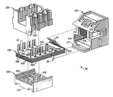
FIG. 6 is an exploded perspective view of a first embodiment of an
electrical connector having time-delayed crosstalk compensation according to
the
invention. The connector 60 comprises a printed wiring board assembly 630,
which is enclosed within dielectric components 610, 620, 640. In particular,
the
assembly 630 includes a multi-layered printed wiring board 600 having
conductive
paths that extend between a jackwire terminal region 635 near a forward edge
631
of the board, and a wire-connection terminal region 634 near a rear edge 633
of the
board.
A number (e.g., eight) of spring jackwires 61 extend from the jackwire
terminal region 635 at an acute angle relative to the top surface of the
wiring board
600. The jackwires 61 connect at their bottom ends to corresponding conductive
paths in the wiring board. The conductive paths are dimensioned and arranged
on
the board layers in such a manner that crosstalk is substantially reduced over
an
entire connection comprising electrical connector 60 and an associated plug
(e.g., a
CA 02245377 2001-04-05
- 10-
modular plug 20 such as shown in FIG. 1). The board may also contain discrete
components such as resist.ars, capacitors and inductors for crosstalk
reduction
between pairs of conductive paths. The bottom ends of the jackwires 61 are
inserted
in metal-plated openings in the bottom surface of the wiring board to connect
with the
conductive paths, and the jac:kwires wrap around a curvilinear forward end of
a
jackwire block 63. Preferably, the bottom ends of the jackwires 61 have a
"needle
eye" construction that allows. the ends to be pushed into the metal-plated
openings
underneath the board 600. These openings have a diameter that is slightly less
than
that of the bottom ends of the jackwires. A reliable electrical connection is
therefore
established between the jackwires and the conductive paths without a need for
soldering.
Insulation-displacement connector (IDC) terminals 62 are mounted at both
rear sides of the wiring board 600 as shown in FIG. 6. Each of the terminals
62
connects to a corresponding conductive path associated with a different one of
the
spring jackwires 61. A pair of terminal housing mounting holes 632 are formed
in the
wiring board 600 along a center line between the rear sides of the board.
A jack frame 610 for the electrical connector 60 may be similar to one
disclosed in U.S. Patent No. .5,897,395 entitled Multi-Position Jack Frame,
issued
April 27, 1999. Alternatively, a jack frame similar to the one disclosed in
the
:?0 above-mentioned U.S. Pat, No. 5,096,442 may also be used for the jack
frame 610.
The frame 610 has an opening or cavity 615 that is dimensioned to receive a
modular
plug in its front end, and a rear opening or cavity 616 that is dimensioned to
receive
the forward edge 631 of the wiring board 600 including jackwires 61. The rear
opening of the jack frame is fornied with a number (e.g., eight) of vertical
slots 618,
'<?5 which receive corresponding ones of the jackwires 61 and guide each
jackwire to
deflect when a plug (not shown) is inserted through the front opening 615 of
the jack
frame. Wire conductors carried by the inserted plug thus establish electrical
contact
with corresponding ones of the jackwires 61.
An electrically insulative or dielectric terminal housing 620, also shown in
:SO FIG. 6, is formed to protect and to permit wire lead access to the wire-
connection
CA 02245377 1998-08-18
-11-
terminal region 634 on top of wiring board 600. The housing 620 may also be
formed of a plastics material that meets all applicable standards with respect
to
electrical insulation an flammability. Such plastics materials include, but
are not
limited to, Polyvinyl Chloride (PVC), Acrylonitrile Butadiene Styrene (ABS),
or
polycarbonate. The housing 620 has a pair of mounting posts 622 that project
from
a bottom surface of the housing. When the housing 620 is aligned with the IDC
terminals 62 on the wiring board 600 and lowered to surround the terminals,
the
mounting posts 622 align with the mounting holes 632 in the board 600 and pass
through them to project from below the board.
1 o A cover 640 is made from a material that may be the same or similar to
that
of the housing 620 and the jack frame 610. Cover 640 is formed to protect the
bottom of the board 600 at the wire-connection terminal region 634. The cover
includes a pair of openings 642 formed along a ~~Pnter line between sides of
the
cover 640, to align with tips of the housing mounting posts 622 that project
below
the wiring board 600. The wiring board 600 is "sandwiched" or captured between
the housing 620 and the cover 640, and the tips of the mounting posts 622 are
preferably joined to the body of the cover by, for example, ari ultrasonic
welding
probe inserted into the cover openings 642 from below the cover. The tips of
the
mounting posts 622 and surrounding cover body melt and fuse with one another
to
2o form solid joints when cooled. With the wiring board 600 thus captured
between
the housing 620 and the cover 640, substantially the entire wire-connection
terminal region 634 of the board is protectively enclosed.
The jack frame 610 has a latch 617 protruding below its rear opening 616.
The cover 640 has a pair of shoulders 647 adjacent the front and back edges of
the
cover. Once the housing 620 is joined to the cover 640 with the wiring board
600
captured between them, the front edge 631 of the wiring board is inserted into
the
rear opening 616 in the jack frame 610 until the latch 617 snaps over and onto
the
adjacent shoulder on the bottom of cover 640.
The actual construction of wiring board 600 is disclosed in FIGS. 7A-7F.
3o An end view of printed wiring board 600 is shown in FIG. 7A having eight
layers
of wiring paths for introducing compensating crosstalk according to the
invention.
Each of the layers comprises one or more metallic paths of thickness dl
positioned
CA 02245377 2001-04-05
-12-
on a dielectric material of thickness d1. Illustratively, d, = 0.04
millimeters (mm) and
dZ = 0.30 mrn. Four double-sided printed wiring boards are joined into a
single unit
600 by epoxy layers in a manner known in the art. Each printed wiring board
comprises a board material, such as FR-4, with conductive paths patterned on
its top
S and bottom surfaces by standard techniques such as photolithography. And
while
eight layers of conductor paths are shown in this illustrative embodiment, it
will be
appreciated that any number can be employed.
FIGS. 7B-7F show top views of the wiring layouts on each of the layers of the
printed wiring board 600. Note that the same wiring layout 603, shown in FIG.
7D, is
used on four (4) layers of the: wiring board. In this particular embodiment of
the
invention, the wiring layout of FIGS. 7B-7F provides three stages of
compensating
crosstalk between wire-pair :l (pins 4, 5) and wire-pair 2 (pins 3, 6), which
are
identified in FIG. 7B. (It is noted that the industry generally refers to pins
3, 6 as
wire-pair 3; e.g., see FIG. 2 of the '647 patent). Reference is briefly made
to FLG. 7D,
which shows discrete capacitors 612 connected between wire-pair 1 and wire-
pair 2 at
the closest possible point to where signals enter layer 603 in the jackwire
terminal
region 635 of board 600, and they comprise the first stage of compensating
crosstalk.
And while these discrete capacitors 612 comprise closely spaced wiring
patterns on a
printed wiring board, stand-alone discrete component structures are shown in
FIGS. 9
:?0 and 10. Additionally, although not immediately apparent from the wiring
paths shown
in FIGS. 7B, 7C, 7E and 7F, there is inductive coupling between wire-pairs 1,
2 in
region 636 in the form of closely spaced inductive loops that face each other.
The self
inductance of these loops improves the return-loss performance of the
connector,
while the inductive coupling between these loops is part of the compensating
;?5 crosstalk.
FIG. 8 is an exploded perspective view of a second embodiment of an
electrical connector having time-delayed crosstalk compensation according to
the
invention. Electrical connector 80 comprises spring block 830, conductor array
CA 02245377 1998-08-18
-13-
800, cover 840 and jack frame 810. Conductor array 800 is made from two lead
frames, one of which includes conductors 801, 803, and the other includes
conductors 802, 804 which are identical to each other. These lead frames are
reversed, left-to-right, with respect to each other and overlaid on each other
in the
manner disclosed in U. S. Patent 5,186,647. These lead frames are positioned
on
the top surface of spring block 830 which includes grooves having the same
pattern
as the overlaid lead frames. Heat is then selectively applied to the grooves
via
ultrasonic welding in order to deform the thermoplastic material from which
the
spring block is made to permanently join the lead frames and spring block
together.
1o IDC terminals 823 are folded down the sides of the spring block while the
conductors in Section 0 of conductor array 800 are wrapped around tongue-like
projection 831 of the spring block 830. Thereafter, cover 840 is joined to the
spring block to create a unitary structure. In this embodiment, spring block
830,
cover 840 and jack frame 810 are all made from a thermoplastic material such
as
PVC. Significantly, conductor leads 802 and 803 cross over each other in two
locations in order to provide two Sections (I and II) where compensating
crosstalk
is introduced in order to cancel the offending crosstalk in Section 0.
Reference is
made to FIG. SA where the same crossover technology is employed on a printed
wiring board to provide two stages of compensating crosstalk.
However, crossover technology is not required in the practice of the present
invention as evidenced by the embodiment of FIG. 9 where discrete components
912 are used to provide compensating crosstalk in Section I. FIG. 9
illustrates a
connecting apparatus 90 that embodies the present invention in a convenient
design. In this embodiment, wire-pair 1 comprising conductors 902, 903 is
straddled by wire-pair 2 comprising conductors 901, 904. These conductors all
extend along a top surface of printed wiring board 900 without crossing over
each
other. In Section 0, offending crosstalk comes from closely spaced wires
within a
modular plug (not shown), modular jack 910, and conductors 901-904 on board
900. Discrete components 912, are used to couple electrical signals between
wire-
pairs 1 and 2 thereby introducing compensating crosstalk between the wire
pairs.
And while only two components 912 are shown, it is understood that they
represent
a combination of resistors and/or capacitors and/or inductors that are
selected to
CA 02245377 1998-08-18
-14-
provide compensating crosstalk, having a predetermined magnitude and phase at
a
given frequency, between wire-pairs 1 and 2 in Section I. As shown in FIG. 9,
a
second stage (Section II) of compensating crosstalk is provided, and it
includes the
crosstalk coming from conductors 901-904 as well as the crosstalk coming from
terminal block 920, which is used for making wire connections and preferably
includes four IDC terminals. FIG. 9 only shows a single jack frame 910 and
terminal block 920, but it is understood that it is common practice to install
many
jack frames and terminal blocks on a single board. Moreover, it is common
practice to have more than four conductive paths between the jack frame and
1 o terminal block and such structures are contemplated by the present
invention.
FIG. 10 is a variation on the embodiment of FIG. 9 in which crossover
technology is combined with discrete component technology to introduce
multiple
stages of compensating crcsstalk according to the present invention. In
Section 0,
offending crosstalk comes from closely spaced wires within a modular plug (not
shown), modular jack 910, and conductors on board 1000. This offending
crosstalk
is substantially canceled in magnitude and phase at a given frequency by
compensating crosstalk from Sections I-III. In Section I, crossover technology
is
illustratively used to introduce compensating crosstalk that is almost 180
degrees
out of phase with the offending crosstalk. In Section II, crossover technology
is
2o used again to introduce compensating crosstalk that is almost 180 degrees
out of
phase with the crosstalk introduced in Section I. And in Section III,
additional
compensating crosstalk is introduced via discrete components 1012 whose
magnitude and phase at a given frequency are selected to substantially
eliminate all
NEXT in connecting apparatus 100.
FIG. 11 is a vector diagram of crosstalk in a three-stage compensation
scheme, according to the invention, for the electrical connector of FIG. 6. In
particular, offending crosstalk vector Ao is substantially canceled by
compensating
crosstalk vectors A" Az, A3 whose magnitudes and polarities are generally
indicated in FIG. 11. It is noted that the offending crosstalk Ao is primarily
3o attributable to the closely spaced parallel wires within the conventional
modular
plug 20 (see FIG. 1), which is inserted into the electrical connector 60 (see
FIG. 6)
of the present invention. The magnitudes of the vectors Ao - A3 are in
millivolts
CA 02245377 1998-08-18
-1S-
(mv) of crosstalk per volt of input signal power. The effective separation
between
stages is designed to be about 0.4 nanoseconds. The following vector
magnitudes
apply to FIG. 11:
Aa = 17.0 mv/volt
A, = 47.6 mv/volt
Az = 47.6 mv/volt
A3 = 17.0 mv/volt
This particular selection of vector magnitudes and phases provides a null at
about
180 MHz in order to reduce NEXT to a level that is 60 dB below the level of
the
1 o input signal for all frequencies below 100 MHz. Obviously, vectors can be
selected to produce one or more nulls at other frequencies in order to meet
particular design objectives.
FIG. 12 is a graph showing calculated NEXT as a function of frequency
using the vector magnitudes discussed in connection with FIG. 11. The present
invention represents the first recognition that delayed compensation stages
can
reduce NEXT to negligible values in practical electrical connectors.
Although various particular embodiments of the present invention have
been shown and described, modifications are possible within the scope of the
invention. These modifications include, but are not limited to, the
introduction of
2o compensating signals within the plug itself and the use of time-delayed
signal
compensation in electrical connecting apparatus other than modular plugs and
j acks.
It is also understood that it is possible to introduce time delay using
discrete
elements (e.g., inductors and capacitors) rather than, or in addition to,
physical
separation along the interconnection path, and that time-delayed signal
compensation can be used between individual conductors as well as pairs of
conductors. It is finally understood that time-delayed signal compensation can
be
used to improve return loss and balance and as well as crosstalk.