Note: Descriptions are shown in the official language in which they were submitted.
CA 02245409 1998-08-24
1
Planar Optical Waveguide
BACKGROUND OF THE INVENTION
The present invention relates to a planar optical waveguide and a method for
manufacturing the same.
Communication systems utilising optical systems having become common
place recently. When first introduced, the optical systems were based on the
use of
optical fibers which were symmetrically round. More recently however, planar
waveguide devices have been introduced due to the ease with which different
types of
device can be formed utilising techniques learned from semiconductor
manufacture.
However, planar waveguides frequently exhibit differing refractive indices
parallel and
perpendicular to the plane of the surface of the substrate. Unpolarised light,
which enters
a birefi-ingent planar waveguide is split into one component in a direction
parallel to and
one component in a direction perpendicular to the surface of the substrate of
the
waveguide and these components propagate at different rates. This makes
optical circuits
more difficult to design because wavelength - selective elements such as
directional
couplers or wavelength multiplexers incorporating reflection gratings can be
optimally
designed for only one polarization direction. This phenomenon is termed by
birefringence and in the case of crystalline planar substrates, the
birefringence results
from the crystalline structure and the selected orientation of the crystals to
the plane.
Amorphous, transparent materials such as glass do not exhibit birefringence
provided
they are stress free.
Much attention has therefore been directed to producing low-birefringence
planar optical waveguides and the technique normally employed is to
manufacture the
waveguides from glass on a essentially planar silicon crystal substrate. With
this method,
the layers of glass are produced at elevated temperature and/or require high
temperature
treatment in order to ensure homogeneity. The result of the high temperature
treatment
C:~~..\WP~h'I'vWPDOCS'SPECS\NORTEL\IS0716.SPC
CA 02245409 2003-07-16
77564-3
2
is that the difference between the thermal expansion co-
efficients of the substrate and the layers coated thereon
therein leads to considerable stresses on cooling and, in
the event of single-sided coating, even to bending of the
silicon crystal substrate. Owing to the well known stress-
optical effect, these stresses bring about birefringence in
the light carrying core of the waveguide. The effect of the
birefringence is shown in Fig. 3 where the peak insertion
losses in all TE and TM modes occur at different
wavelengths.
A number of different proposals have been made to
overcome this problem and while some techniques are capable
of achieving very low polarisation sensitivity (less than or
equal to 0.05 nm for arrayed waveguide demultiplexers~ they
are not suitable for low cost/high volume production.
DE-A-4433738 discloses a technique which is stated to result
in low-birefringence and involves making the thermal
coefficient of expansion of the optical core material the
same as the temperature coefficient of expansion of the
silicon substrate. This document is alleged to result in a
reduction in the polarisation sensitivity in the region of
0.1 to 0.2 nm which is still not sufficiently good for
practical purposes.
SUMMARY OF THE INVENTION
It is an object of the present invention to
provide a planar optical waveguide device which exhibits low
birefringence i.e. low polarisation sensitivity of the order
of 0.05 nm or less.
The present invention provides a planar optical
waveguide comprising at least two cladding layers on a
CA 02245409 2006-05-29
77550-236
3
substrate and at least one core layer disposed between the
cladding layers, one of the cladding layers comprising an
overcladding layer, said core layer having a higher
refractive index than the refractive index of the cladding
layers, wherein the overcladding layer has a thermal
coefficient of expansion substantially matched with the
thermal coefficient of expansion of the substrate and not
matched with the thermal coefficient of expansion of the
core layer.
It has been found that a device as specified above
will produce a polarisation sensitivity of only 0.03 to
0.05 nm.
According to another aspect the invention provides
a process for fabricating a planar optical waveguide
comprising forming an undercladding layer on a major surface
of a substrate, forming a waveguide core on the
undercladding layer, said core having a higher refractive
index than the refractive index of the undercladding layer,
and forming an overcladding layer over the waveguide core,
the overcladding layer being doped in order to produce a
thermal coefficient of expansion substantially matched with
the thermal coefficient of expansion of the substrate and
not matched with the thermal coefficient of expansion of the
core.
Preferably, the substrate is formed of silicon and
the layers provided thereon contain silicon oxide.
In a preferred embodiment the overcladding layer
is doped with material containing germanium, boron and/or
phosphorous.
The undercladding layer may also be doped with
material containing germanium, boron and/or phosphorous.
CA 02245409 2006-05-29
77550-236
3a
Each layer may be formed by a process such as
PECVD, LPCVD, APCVD or FHD.
Preferably, the thermal coefficient of expansion
of the overcladding layer is substantially equal to but no
greater than that of the substrate.
Preferably the substrate is formed of silicon and
the thermal coefficient of expansion of the overcladding
layer is in the range 30 to 35x10-'/°C.
We have found that the thermal coefficient of
expansion of the undercladding and of the optical core
material can vary widely from between 10 and 30x10-'/°C and
the device will still exhibit low birefringence.
BRIEF DESCRIPTION OF THE DRAWINGS
In order that the present invention be more
readily understood, an embodiment thereof will now be
described by way of example only with reference to the
accompanying drawings, in which:-
Fig. 1 shows a cross sectional side view of a
waveguide device according to the present invention;
Fig. 2 shows diagrammatically an arrayed grating
wavelength demultiplexer;
Fig. 3 shows a diagram of insertion loss against
wavelength for both the TE and TM modes;
Fig. 4 shows a diagram of insertion loss against
wavelength for both the TE and TM modes for a device
according to the present invention; and
CA 02245409 2003-07-16
77564-3
3a
Each layer may be formed by a process such as
PECVD, LPCVD, APCVD or FHD.
Preferably, the thermal coefficient of expansion
of the overcladding layer is substantially equal to but no
greater than that of the substrate.
Preferably the substrate is formed of silicon and
the thermal coefficient of expansion of the overcladding
layer is in the range 30 to 35E-7.
We have found that the thermal coefficient of
expansion of the undercladding and of the optical core
material can vary widely from between 10 and 30E-7 and the
device will still exhibit low birefringence.
BRIEF DESCRIPTION OF THE DRAWINGS
In order that the present invention be more
readily understood, an embodiment thereof will now be
described by way of example only with reference to the
accompanying drawings, in which:-
Fig. 1 shows a cross sectional side view of a
waveguide device according to the present invention;
Fig. 2 shows diagrammatically an arrayed grating
wavelength demultiplexer;
Fig. 3 shows a diagram of insertion loss against
wavelength for both the TE and TM modes;
Fig. 4 shows a diagram of insertion loss against
wavelength for both the TE and TM modes for a device
according to the present invention; and
CA 02245409 2003-07-16
77564-3
3b
Fig. 5 shows a diagram of insertion loss against
wavelength for the TE mode of a 16 channel device according
to the present invention.
DETAILED DESCRIPTION OF PREFERRED EMBODIMENTS
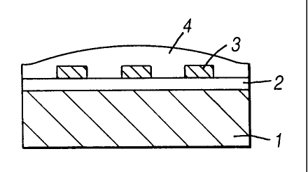
A planar optical waveguide device as shown in
Fig. 1 comprises a substrate 1 usually in the form of a
single silicon crystal on which a cladding layer 2 is formed
on one side. The layer 2 usually contains silicon dioxide
(Si02) and may be thermally grown or deposited by a process
such as PECVD, LPCVD, APCVD or FHD.
The layer 2 is normally more than 10~m in
thickness and is consolidated by annealing at temperatures
above 1100°C. One or more optical core elements are formed
in a layer 3. Once more the layer 3 contains Si02 but the
refractive index of the layer 3
CA 02245409 2006-05-29
77550-236
4
is higher than the refractive index of the layer 2.
Typically the difference in refractive index is of the order
of 5x10⁻³ to 20x10-3 and is obtained by doping the core layer
with germania, phosphorous oxide, boron oxide, or
combinations thereof. Thereafter, an overcladding layer 4
is provided which will be seen to cover three sides of the
optical core layer 3. The overcladding layer 4 has the same
refractive index as the undercladding layer 2 and is formed
using any of the techniques mentioned in relation to the
undercladding Layer 2.
The above structure is basically conventional but
the present invention differs from the conventional
structure insofar as the overcladding layer 4 is doped with
a suitable material so as to achieve a thermal coefficient
'15 of expansion which is very close to the thermal coefficient
of expansion of the substrate 1. How the doping material is
chosen and how the quantity of doping is determined will now
be described.
It is known that doping silicon oxide with a
dopant such as boron oxide and phosphorous oxide will
increase the thermal coefficient of expansion of the
material so doped. It is also known that the stress in a
layer is related to the thickness T of the layer and the
thickness D, module of elasticity E and Poisson coefficient
V of the substrate by the equation o = E.D2/[6(1-v).R.T]
where R is the measured curvature of the
combination. Using the stress-optical coefficient K, the
birefringence B can be obtained since
B = K. a = nTE - nTM where nTE is the refractive
index of the TE mode and nTE is a refractive index for the TM
mode of the optical core. It is known that the stress-
CA 02245409 2006-05-29
' 77550-236
optical coefficient K is approximately 3.5 nm/cm/bar for
Si02 .
On the basis of this background information, a
test device having the basic structure shown in Fig. 1 was
5 prepared and tested in the configuration shown in Fig. 2.
The curvature R of the overcladding was measured using a
profilometer. An overcladding layer of thickness 15 um was
used. The amount of doping and the dopant material were
changed in successive experiments until the measured
curvature indicated that birefringence was reduced to a
minimum. It was found on analysis from a satisfactory test
that the thermal coefficient of expansion of the
overcladding layer for low birefringence was of the same
order as the thermal coefficient of expansion of the
substrate 1; in other words of the order of 35x10-'/°C.
Preferably, the doped overcladding layer should be in a
state of low compressive stress compared to the substrate,
in order to avoid stress cracking due to defects.
The test also showed that an overcladding layer 4
having a thermal coefficient of expansion of around
28x10-'/°C gave a wavelength shift due to polarisation of the
order 0.2 to 0.25 nm which is deemed not satisfactory for
practical devices. This is shown in Fig. 3. It was also
found that doping the undercladding layer 2 with boron or
phosphorous material to produce a thermal coefficient of
expansion of the order of 22x10-'/°C and doping of the core
layer 3 with boron phosphorous or germanium containing
material to produce thermal coefficients of expansion
varying from 13 to 30x10-'/°C showed that without the correct
doping of the overcladding 4 to match the thermal
coefficient of expansion of the substrate, it was not
possible to achieve polarisation sensitivity below 0.1 nm.
CA 02245409 2006-05-29
77550-236
6
The results of the test were then noted and
practical devices produced using the same starting materials
as the test but by doping the overcladding layer 4 with the
appropriate amount of dopant to produce a thermal
coefficient of expansion of the order 35x10-'/°C which is
close to that of the silicon substrate. The effect in the
graphs of insertion loss for the TE and TM modes as a
function of wavelength is shown in Fig. 4.
Further tests have shown that a thermal co-
efficient of expansion of 33.8x10-'/°C gave satisfactory
results as did 37.3x10-'/°C. It is considered advisable to
keep the thermal co-efficient of expansion of the
overcladding layer 4 to be less than or equal to that of the
substrate 1 so that the layer 4 stays in a state of
compressive stress.
The benefits of this invention are that 16 channel
wavelength demultiplexors can be produced which have
insertion losses as shown in Fig. 5. The graphs of
insertion loss in this figure are true for both the TE and
TM modes.