Note: Descriptions are shown in the official language in which they were submitted.
CA 02245498 1998-08-OS
WO 97128925 PCT/US97/01266
a
-1-
LAPPING AND POLISHING METHOD AND APPARATUB FOR
PLANARIZING PHOTORESIST AND METAL MICROSTRUCTURE LAYERB
FIELD OF THE INVENTION
This invention pertains generally to the field of
semiconductor and micromechanical devices and processing
techniques therefor, and particularly to methods and
devices for removing material from photoresist and metal
:microstructure layers to planarize and polish the layers
for the formation of multi-level and precision engineered
1d microminiature structures.
BACKGROUND OF THE INVENTION
Deep X-ray lithography involves a substrate which
is covered by thick photoresist, typically several hundred
microns in thickness, which is exposed through a mask by X-
25 rays. X-ray photons are much more energetic than optical
photons, which makes complete exposure of thick photoresist
films feasible and practical. Furthermore, since X-ray
photons are short wavelength particles, diffraction effecta
which typically limit device dimensions to two or three
2fl wavelengths of the exposing radiation are absent for mask
dimensions above 0.1 micron. Additionally, X-ray photons
are absorbed by atomic processes, therefore, standing wave
problems, which typically limit exposure of thick
photoresist by optical means, become a non-issue for X-ray
CA 02245498 1998-08-OS
WO 97128925 PCTlUS97/01266
-2 -
exposures. The use of a synchrotron for the X-ray source
yields high flux densities of several watts per square
centimeter, combined with excellent collimation to produce
thick photoresist exposures without any horizontal run-out.
Locally exposed patterns will therefore produce vertical
photoresist walls if a developing system with very high
selectivity between exposed and unexposed photoresist is
used. This requirement is satisfied by polymethyl-
methacrylate (PMMA) as the X-ray photoresist and an aqueous
developing system. See: H. Guckel, et al., "Deep X-Ray
and UV Lithographies for Micromechanics", Technical Digest,
Solid State Sensor and Actuator Workshop, Hilton Head,
S.C., June 4-7, 1990, pp. 118-122.
Deep X-Ray lithography may be combined with
electroplating to form high aspect ratio structures. This
requires that the substrate be furnished with a suitable
plating base prior to photoresist application. Typically,
this involves a sputtered film of adhesive metal such as
chromium or titanium which is followed by a thin film of
the metal which is to be plated. The photoresist layer is
then applied over the plating base. Exposure through a
suitable mask and development are followed by
electroplating. This results, after clean-up, in fully
attached metal structures with very high aspect ratios.
Such structures were reported by W. Ehrfeld and co-workers
at the Institute for Nuclear Physics at the University of
Rarlsruhe in West Germany. Ehrfeld termed the process
"LIGA", based on the first letters of the German wards for
lithography and electroplating. A general review of the
LIGA process is given in the article by W. Ehrfeld, et al.,
r'LIGA Process: Sensor Construction Techniques Via X-Ray
Lithography", Technical Digest, IEEE Solid State Sensor and
Actuator Workshop, 1988, pp. 1-4.
The addition of a sacrificial layer to the LIGA
grocess facilitates the fabrication of fully attached,
partially attached, or completely free metal structures.
This makes possible the assembly in micromechanics of
nearly arbitrary 3-dimensional structures and machines.
CA 02245498 1998-08-OS
''VO 97/25925 PCTJUS97/0126C
-3-
See H. Guckel, et al., "Fabrication of Assembled
Micromechanical Components Via Deep X-Ray Lithography,"
Proceedings of IEEE Micro Electro Mechanical Systems,
~,fanuary 30-February 2, 1991, pp. 74-79. See also U.S.
Patent Nos. 5,206,983, and 5,327,033, to Guckel, et al.,
describing micromechanical devices and methods of
manufacturing same.
It is possible to extend the LIGA process, with
ar without a sacrificial layer, by performing several X-Ray
exposures of multiple photoresist layers and by
electroplating multiple additional layers of metal after
each exposure. Such multilevel processing allows complex
metal structures to be formed in microminiature dimensions.
Structures which may be formed using multilevel processing
include structures having overhanging portions, and tubular
structures which can be utilized for hydraulic and
pneumatic applications. Such structures may be formed on a
sacrificial layer, to allow complete removal of the parts
from the substrate for subsequent assembly into even more
complex structures.
In LIGA processing, a photoresist layer is formed
to have recesses which are filled with electroplated metal.
However, in electroplating such a layer, the plating rate
~i.s dependant on the pattern of the photoresist recesses
which are being ffilled. Uniform deposition of metal is
very difficult to achieve, and, therefore, direct height
control, i.e., dimensional control in the z-dimension, of
the deposited metal is very difficult. However, precise
height control is needed for processing precision
3o engineered single and mufti-level structures. For example,
precise height control is needed to fabricate precision
engineered micro-mechanical devices, such as springs, in
single level processing. The electroplated metal will also
have an uneven surface. Multilevel processing requires re~-
~35 p~lanarization of the electroplated metal in order to
provide a substantially flat, uniform, and smooth surface.
Such a surface is better suited to have a second layer
electroplated thereon than the rough surface of an as-
CA 02245498 1998-08-OS
WO 97128925 PCT/US97J01266
-4-
plated metal. Planarization is also required for proper
adhesion of additional photoresist layers. Multilevel
processing, and accurate dimensional control in the z
(vertical) dimension in processing precision engineered
micro parts is, therefore, essentially impossible without
replanarization.
One method of re-planarizing an electroplated
metal layer involves the machining, e.g., mechanical
grinding or milling, of the electroplated metal layer,
using commercially available micromilling equipment such as
a diamond fly cutter, to achieve a substantially flat and
smooth surface. However, such mechanical machining is
difficult or impossible where a polymer photoresist remains
adjacent the electroplated metal structure. Machining
generally cannot be done through both the photoresist and
the metal. The photoresist is relatively weak
mechanically, and will shred and tear as it is being
milled. Also, the photoresist is not strong enough to
provide horizontal support to the relatively small, and
potentially fragile, metal microstructure. If the
photoresist were removed, and machining of the now isolated
metal structure were attempted, such machining would be
extremely difficult and would risk substantial damage to
the metal structure, such as ripping portions of the metal
structure from the substrate.
One solution to this problem was presented in
U.S. Pat. No. 5,190,637, to Henry Guckel, entitled
Formation of Microstructures by Multiple Level Deep X-Ray
Lithography with Sacrificial Metal Layers. In carrying out
the process of this invention, a primary metal layer is
established using the normal LIGA process by electroplating
the metal into the recesses of a photoresist layer. The
photoresist layer is then removed in its entirety. A
secondary metal, which constitutes a sacrificial metal, is
then electroplated over the previously deposited first
layer of primary metal. The secondary metal is selected so
that it will be differentially etched by a selected etchant
which does not substantially attack the primary metal. The
CA 02245498 1998-08-OS
~'O 97/28925 PCT/US97/OI266
_g_
exposed surface of the deposited secondary metal is then
machined down to a height which exposes the first metal,
and which achieves a substantially flat, uniform surface
,. extending across the primary and secondary metals.
Machining also allows the thickness of the first layer of
primary metal to be closely controlled. After the first
layer of primary and secondary metals has been machined
down to the desired height, additional layers may be formed
on top of the first layer using the same procedure
to employing primary and secondary metals. A microstructure
is thereby formed of multiple primary metal layers. The
secondary, sacrificial, metal may be removed from around
the primary metal structure using a selective etchant. The
utilization of the secondary or sacrificial metal to
I5 completely cover each layer of the primary metal
facilitates the machining of both the primary and secondary
metals because of the mechanical stability which the
secondary metal affords to the primary metal which it
surrounds and supports. However, the formation of
20 microstructures using this method requires a separate
electroplating step to be performed at each level, and a
final etching step to be performed to remove the
sacrificial metal, thereby increasing the complexity of the
metal microstructure fabrication process.
25 Multilevel processing to form metal micro-
structures may also be achieved using preformed photoresist
sheets which are adhered together, and adhered to a
substrate, before the electroplating process takes place.
This process is described in U.S. Pat. No. 5,378,583, to
30 Henry Guckel, et al., entitled Formation of Microstructures
Using a Preformed Photoresist Sheet. The use of preformed
b
photoresist sheets allows much thicker photoresist layers
to be used than is possible with traditional photoresist
layers which are cast in liquid form directly onto a
35 substrate and then annealed. The preformed photoresist
sheet layers may be exposed in a pattern, and may, but need
not, be developed before they are adhered together or
adhered to a substrate. Each layer may also be
CA 02245498 1998-08-OS
WO 97J28925 PCTIi3S97/01266
-6-
mechanically milled, using commercially available milling
equipment, to a desired thickness. For example, a
preformed photoresist sheet may be exposed to X-ray
radiation to a depth only partially through the photoresist
y
sheet, adhered to a substrate or second photoresist sheet,
and then milled down to expose the X-ray exposed portion of ,
the sheet. Exposed, developed, and milled photoresist
sheets may be used individually, or combined in multiple
layers, to form photoresist microstructures. Mufti-layer
photoresist structures may be adhered to a substrate as
molds for the formation of electroplated metal
microstructures or may, themselves, have independent
utility. Milling of photoresist sheets in the conventional
manner, however, introduces sheer forces which may, as
described above, shred, tear, or otherwise damage the
photoresist sheet.
SUM~M~1RY OF THE INVENTION
In accordance with the present invention
planarizing of photoresist and metal microstructure layers
is achieved by lapping and polishing under controlled
conditions. Lapping is used to remove material from the
layer to planarize the layer. Polishing may then be used
to apply a desired smooth finish to the layer surface. The
present invention provides for z-dimensional height control
of metal microstructures, which is necessary for the
fabrication of precision microstructure devices, such as
springs, in single level processing. The present invention
also provides for the re-planarization of a photoresist and
deposited metal layer, to bring the layer to a desired
height and to smooth the surface of the layer, in
preparation for the application of a subsequent photoresist
and metal layer. Thereby, the present invention
facilitates multilevel microstructure processing in
addition to precise z-dimensional control and stability for
single layer processing. The lapping and polishing method
and apparatus of the present invention removes all excess
CA 02245498 1998-08-OS
V~VO 97/28925 PCT/US97/01266
-7-
metal and photoresist above the designed height from the
photoresist-metal layer. After planarization in accordance
with the present invention, the heights of the photoresist
and metal will be the same. The planarized photoresist and
metal surfaces will exhibit a smooth, nearly optical
:Finish. The lapping and polishing method and apparatus of
ithe present invention introduces relatively small shear
forces, thereby preventing damage to the photoresist due to
shredding or tearing, or loss of adhesion of the
l0 ~photoresist or metal layer from a substrate, and
:Facilitating the production of z-dimension controlled
vertically oriented structures that are much taller than
they are wide.
The lapping and polishing method of the present
.invention employs a lapping machine that is furnished with
a lapping plate having a lapping surface made of a soft
metal, such as a copper composite. The lapping plate is
conditioned to have a lapping surface that is preferably
;slightly concave in shape. The surface of the lapping
plate is preferably conditioned using a diamond
conditioning ring which produces ridges in the lapping
surface. The grit of the diamond conditioning ring is
selected based upon the particle size in the diamond slurry
that will be used during the polishing process. After
conditioning with the diamond conditioning ring, the
lapping plate surface is thoroughly cleaned. Free diamonds
in a liquid slurry are then sprayed onto the plate. A
second conditioning ring, preferably made of a ceramic, is
used to help embed the fine size diamonds from the slurry
into the rough ridged surface of the lapping plate. The
lapping plate is thereby made ready to remove material from
a workpiece having photoresist or metal layers that need to
be planarized.
The piece to be planarized may be mounted onto
4
the lapping plate using various fixtures and techniques.
for example, a commercial vacuum chuck hold down fixture
having a thickness monitoring gauge, or wax mounting on a
SUBSTITUTE SHEET (RULE 26)
CA 02245498 1998-08-OS
WO 97!28925 PCT/LT897/01266
_-7~1_
flat steel or glass mounting plate, may be used to mount
the workpiece onto the lapping plate. Weights are
preferably applied to the mounting fixture to increase the
r
SUBSTITUTE SHEET (RULE 26)
CA 02245498 1998-08-OS
'VO 97128925 PCT/US97/01266
-g-
contact pressure between the lapping plate and the
workpiece to a desired level. During the lapping process,
the diamond slurry is periodically sprayed onto the lapping
,. plate, and embedded into the lapping plate surface by the
ceramic conditioning ring, as the lapping plate surface is
rotated against the surface to be planarized. Shear
forces, and the final finish of the planarized surface, are
determined, in part, by the diamond size in the slurry.
'fhe amount of material removed from the workpiece is
to monitored during the lapping process. After an extended
lapping duration, the cutting rate will decrease as the
ridges formed in the surface of the lapping plate are worn
out. At this point, the lapping plate surface may be
cleaned and reconditioned using the diamond and ceramic
conditioning rings.
For some metals, the lapping process of the
present invention may cause metal from microstructures
formed on a substrate to smear into adjacent photoresist
areas. In such cases, a finish lapping step may be
employed using a fine diamond slurry and lapping with
moderate weight for a prolonged period of time to remove
any smearing that exists. This finish lapping step is only
used after the photoresist-metal layer has been reduced to
within la-15 ~tm of the final desired height of the micro
part.
After lapping, and finish lapping if necessary, a
polishing step may be employed. The polishing step uses a
polisher with a hard (stainless steel) polishing plate
covered by a polishing cloth saturated with a diamond
3o slurry. The polishing step cuts an additional
3-4 ~cm of material from the layer being polished to produce
a mirror-like finish on the workpiece at the specified
r
photoresist-metal height.
The lapping and polishing method and apparatus of
the present invention may also be used to remove material
from preformed photoresist sheets, to planarize the surface
of the sheets, and to provide the desired mirror-like
finish to the sheets. Lapping and polishing of photoresist
CA 02245498 1998-08-OS
WO 97/28925 PCT/US97/01266
-g-
layers using the method and apparatus of the present
invention enhances the ability to adhere photoresist sheets
together by solvent bonding. Lapping and polishing of a
photoresist sheet may be accomplished either before or
~.fter the photoresist sheet has been exposed to X-rays,
either before or after exposed portions of the photoresist
have been developed, and either before or after the
photoresist sheet has been adhered to other sheets or
applied to a substrate. Photoresist sheets that are
l0 planarized in accordance with the lapping and polishing
method of the present invention may be used in combination
with other similarly processed photoresist sheets to form
photoresist laminate structures, having independent
utilities, or, when adhered to a substrate, for producing
multilevel electroplated metal microstructures.
Further objects, features, and advantages of the
invention will be apparent from the following detailed
description when taken in conjunction with the accompanying
drawings.
BRIEF DESCRIPTION OF THE DRAWINGS
In the drawings:
Fig. 1 is a simplified illustrative side view of
a substrate with a plating base layer and photoresist layer
formed thereon.
Fig. 2 is an illustrative view showing the
photoresist and substrate of Fig. 1 exposed through an X-
ray mask to X-ray radiation.
Fig. 3 is an illustrative view showing the
substrate and photoresist of Fig. 2 after the exposed
photoresist has been developed.
Fig. 4 is an illustrative view showing the
substrate and photoresist of Fig. 3 after a metal ,
microstructure has been electroplated onto the plating base
in the area from which the exposed photoresist has been
removed.
CA 02245498 1998-08-OS
'CVO 97/28925 PCT/US97/01266
-10-
Fig. 5 is an illustrative view showing the
substrate, photoresist, and metal microstructure of Fig. 4
after the photoresist-metal layer has been re-planarized
'' using the lapping and polishing method and apparatus of the
present invention.
Fig. 6 is an illustrative view of the substrate
and planarized photoresist-metal layer of Fig. 5 with a
second layer of photoresist formed thereon.
Fig. 7 is an illustrative view showing the multi-
IO layered structure of Fig. 6 after the second layer of
photoresist has been exposed through an X-ray mask to X-ray
radiation and after the exposed portion of the second layer
of photoresist has been developed.
Fig. 8 is an illustrative view showing the multi-
7_ayer structure of Fig. 7 wherein a second metal layer has
been electroplated into the portion of the second layer of
photoresist which has been removed and onto the first
electroplated metal layer.
Fig. 9 shows the mufti-layer structure of Fig. 8
after the second photoresist-metal layer has been re-
planarized using the lapping and polishing method and
apparatus of the present invention.
Fig. 10 illustrates the use of a flatness gauge
to measure the flatness of a concave lapping plate to be
used in accordance with the present invention.
Fig. I1 illustrates the positioning of a diamond
conditioning ring on the concave lapping plate of Fig. l0
to condition the lapping plate in accordance with the
present invention.
Fig. 12 illustrates the use of a flatness gauge
to measure the flatness of a convex lapping plate to be
used in accordance with the present invention.
Fig. 13 illustrates the positioning of a diamond
. conditioning ring on the convex lapping plate of Fig. 12 to
condition the lapping plate in accordance with the present
invention.
Fig. 14 illustrates the use of a flatness gauge
to measure the flatness of a lapping plate having a
CA 02245498 1998-08-OS
WO 97128925 PCT/US97/OI266
-11-
polishing surface which is concave between the center and
outer edge of the lapping plate to be used in accordance
with the present invention.
Fig. 15 illustrates the positioning of a diamond
conditioning ring on the lapping plate of Fig. 14 for
conditioning the lapping plate in accordance with the
present invention.
Fig. 16 illustrates the further conditioning of
the lapping plate in accordance with the present invention
using a spray of diamond slurry and a ceramic conditioning
ring.
Fig. 17 illustrates the relative positions on the
lapping plate of the diamond slurry spray, the ceramic
conditioning ring, and a workpiece during planarization of
the workpiece in accordance with the lapping and polishing
method of the present invention.
Fig. 18 is an illustrative view of a substrate
having a photoresist-metal layer which has been initially
planarized in accordance with the present invention,
showing smearing of the electroplated metal which may
result.
Fig. is is an illustrative plan view of a
mounting plate upon which a workpiece to be lapped has been
mounted along with glass support pieces.
Fig. 20 is an illustrative cross-sectional view
of Fig. 19 taken along the line 20-20.
Fig. 21 is an illustrative side view of a
relatively thick preformed photoresist sheet being exposed
through an X-ray mask to X-ray radiation.
Fig. 22 is an illustrative view of two relatively
thick preformed photoresist sheets which have been exposed
to X-rays in the manner illustrated in Fig. 21 and which ,
have been developed to remove the exposed photoresist.
Fig. 23 is an illustrative view showing the two ,
layers of preformed, exposed, and developed photoresist
sheets of Fig. 22 bonded together at their exposed
surfaces.
CA 02245498 2001-05-23
-12-
Fig. 24 is an illustrative view of the
photoresist layers of Fig. 23 after the top layer has been
planarized down using the lapping and polishing method and
apparatus of the present invention to fully expose the
developed regions of. the top photoresist layer.
Fig. 25 is an illustrative view of the
photoresist layers of Fig. 24 with the addition of another
photoresist layer which is formed in the manner illustrated
above with respect to Figs 21-24.
l0 Fig. 26 is an illustrative view of the multi-
layer photoresist laminate of Fig. 25 with the free surface
of the top layer bonded to a substrate and before lapping
and polishing o. the thick photoresist layer in accordance
with the lapping and polishing method and apparatus of the
15 present invention.
DETAILED DESCRIPTION OF THE INVE<~TION
The lapping and polishing method and apparatus of
the present invention may be utilized in the formation of
single and multi-level microstructures carried out in LIGA
20 processes and extensions thereof. An exemplary process for
carrying out the formation of a metal microstructure
employing the lapping and polishing method of the present
invention is described briefly below. The details of LIGA
processing itself are known to those having skill in the
Z5 art. A detailed description of an exemplary process for
carrying ou~ the production of micromechanical structures
is described, for example, in U.S. Patent No. 5,190,637, to
Henry Guckel, entitled Formation of Microstructures by
Multiply Level Deep X-Ray Lithography with Sacrificial
30 Metal Layers.
A basic process employing the lapping and
polishing method and apparatus of the present invention to
fore a multilevel metal microstructure is illustrated with
respect to the views of Figs. 1-9.. With reference to Fig.
3J 1, a substrate 30 is provided which may comprise a variety
CA 02245498 2001-05-23
-13-
of materials, including semi-conductors, insulators, and se
forth. Typically, a metal plating base 31 will be
deposited onto the ton surface of the substrate 30, such as
by sputtering. The substrate 30 could be composed of a
conductive metal, in which case no plating base may be
necessary. For the formation of parts to be freed from the
substrate 30, a sacrificial release layer (not shown) may
be used beneath the plating base layer 31. A photoresist
layer 33, for example, polymethylmethacrylate (per), is
then applied to the substrate. Depending on the type of
radiation used, the depth of exposure desired, and the
properties of available photoresists, it is apparent that
positive or negative photoresist may be used. The
photoresist layer 33 may be cast-on to the desired
thickness, or may be applied as a preformed photoresist
sheet. The use of prefor:ned photoresist sheets in the
formation o° metal microstructures is described in morn
detail in L?.S. Patent No. 5,378,583, to Henry Guckel, et
al., entitled Formation of Microstructures Using a
Dreformed Photoresist Sheet. If a preformed
photoresist sheet is used it may be exposed to radiation
and development before being adhered to the substrate 30.
As illustrated in Fig. 2, an X-ray mask 34 having
X-ray absorbing patterns 35 formed thereon, provides a
pattern exposure from synchrotron radiation X-rays 36 to
provide an exposed pattern 37 in the photoresist sheet 33.
Although exposure of the photoresist 33 to radiation
consisting of synchrotron X-rays 36 is preferred, to obtain
structures of maximum depth and minimum run-out, it is
apparent that the process may be used with other radiation,
such as ultraviolet (UV) or non-synchrotron source X-rays,
where ti:inner structures aze acceptable. The exposed
photoresist 37 is then developed using a highly selective
developer :.o remove the exposed photoresist 37, leaving, as
3~ shown in Fig. 3, a patterned portion 38 of the plating base
31 exposed .
CA 02245498 1998-08-OS
~~VO 97128925 PCT/US97/01266
-14-
As shown in Fig. 4, a metal microstructure 39 is
then electroplated onto the exposed portion 38 of the
plating base 31. Note that a metal structure may be packed
into the voids formed in the photoresist, rather than
electroplated. A typical metal microstructure 39 may be
made out of nickel; however, a variety of other metals may
also be used to form the microstructure 39, as is known in
the art. In the electroplating process, the plating rate
is dependant, in part, upon the pattern in the photoresist
33 that is used to form the microstructure. Uniform
deposition of the electroplated metal 39 is very difficult
to achieve. Therefore, direct height control of the
electroplated metal structure 39 is very difficult,
resulting in a microstructure 39 having an uneven upper
I5 surface. As illustrated in Fig. 4, z-dimension variation
in the electroplated structure 39 can be extreme. This is
especially apparent near the walls of the well formed by
the photoresist layer 33, where additional material may be
deposited having z-dimension thickness on the order of the
final desired microstructure height itself.
Tight control of the z-dimensional height of the
metal microstructure 39 is necessary in order to fabricate
precision microstructure devices, such as springs, in
single level processing. Moreover, the formation of
microstructures using multilevel processing requiresthat
the first photoresist-metal layer be planarized prior to
securing subsequent photoresist-metal layers. Re-
planarization is needed to properly adhere a subsequent
photoresist layer to the first photoresist-metal layer
below, and for proper adhesion of a second electroplated
metal layer onto the first layer. Precise engineering and
~ multilevel processing without re-planarization are
typically not possible.
Thus, the next step in the formation of a metal
microstructure, for either single level or multilevel
processing, is the re-planarization of the photoresist-
metal layer using the Zapping and polishing method and
apparatus of the present invention. The resulting
CA 02245498 1998-08-OS
WO 97!28925 PCT/CTS97/01266
-15-
structure, having re-planarized surface 40, is shown in
Fig. 5. The lapping method and apparatus of the present
invention removes all excess metal from the microstructure
39 above the designed height. Some of the photoresist 33
is also removed at essentially the same rate, resulting,
after re-planarization, in the photoresist layer 33 and
metal microstructure 39 having the same thickness. The
polishing method and apparatus of the present invention
provides a planarized photoresist-metal surface structure
40 that exhibits a nearly optical ffinish. During the
lapping and polishing process, shear forces applied to the
photoresist 33 and microstructure 39 are kept small to
prevent loss of adhesion between the microstructure 39 or
photoresist 33 and the plating base 31 or substrate 30
beneath them. This facilitates the fabrication of
vertically dimensioned microstructures that are
significantly more high than wide. For example, the
lapping and polishing method of the present invention has
been used in the fabrication of electrostatic activators
including 350 micron tall posts that are 100 microns in
diameter. Reduced shear forces also prevent tearing,
shredding, or other damage to the surface of the
photoresist 33. The lapping and polishing method and
apparatus of the present invention are described in more
detail below.
After the photoresist-metal surface 40 has been
re-planarized using the lapping and polishing method and
apparatus of the present invention, the excess photoresist
33 and plating base 31 may be removed, the microstructure
39 may be removed from the substrate 30 (using a
sacrificial release layer), or the microstructure
fabrication process may proceed for the formation of a
multilevel microstructure. As shown in Fig. 6, a second
layer 4~. of photoresist may be applied on top of the
planarized photoresist-metal surface 40. The smooth
surface 40, having been lapped and polished in accordance
with the method and apparatus of the present invention,
allows for better adhesion between the photoresist layers
CA 02245498 1998-08-OS
V~'O 97J28925 PCTIUS97/01266
-16-
33 and 41. As described above, the second photoresist
layer 41 may be cast on in a traditional manner, or applied
as a preformed photoresist sheet to the re-planarized
" surface 40. As noted above, if a preformed photoresist
sheet is used to form the second photoresist layer 41, the
' photoresist sheet may be exposed to radiation and developed
before being applied to the planarized photoresist-metal
surface 40. The second photoresist layer 41 is then
exposed to X-rays in a pattern using an X-ray mask, and
developed to form a structure, such as is shown in Fig. 7,
wherein a portion of the second photoresist layer 41 is
removed to expose the planarized surface 40 of the first
metal microstructure layer 39. A second layer of metal 42
is then electroplated onto the first metal layer 39 to form
a multilevel microstructure as shown in Fig. 8. As
discussed above, the electroplating process does not allow
z-dimensional height control of the deposited metal 42.
Variations in the height of the deposited structure 42 can
be extreme. The second photoresist-metal layer may,
therefore, preferably be re-planarized, using the lapping
and polishing method and apparatus of the present
invention, to remove excess metal from the second metal
layer 42, to reduce the second metal layer 42 to the
designed height, and to re-planarize the photoresist-metal
layer so that the photoresist and metal thicknesses are the
same and so that the photoresist and metal surfaces exhibit
a nearly optical finish. The resulting structure, having a
re-pianarized surface 44 on the second photoresist-metal
layer, is shown in Fig. 9. The second surface 44 is thus
now prepared for the application of additional photoresist
and metal layers, in the manner described above, for the
~ formation of microstructures having even more metal layers.
The process may also be stopped at this point, and the
remaining photoresist layers 33 and 41 removed to provide a
free-standing multilevel metal microstructure composed of
the two metal layers 39 and 42. Also, the metal
microstructure may be removed from the substrate 30, to
CA 02245498 1998-08-OS
WO 97/28925 PCT/C1S97/01266
-3?-
form a freed metal microstructure, using a sacrificial
release layer (not shown).
The present invention employs a diamond lapping
and polishing technique in which re-planarization of ~
photoresist and metal surfaces, and polishing to a nearly
optical finish, is achieved while shear forces are
minimized. In the following description, the term
"lapping" is used to refer to the removal of material from
a surface, at a relatively high rate, using diamonds
embedded in a lapping plate. "Polishing" refers to the
application of a smooth optical finish to a surface using a
free non-embedded diamond slurry typically embedded in a
polishing cloth. Polishing is used following lapping, and
removes little additional material from the surface being
polished.
In lapping a work piece in accordance with the
present invention, a conventional lapping machine, such as
an LM 115 Hyprez Lapping Machine, available from Engis
Corp., Wheeling, Illinois, is used. The lapping machine is
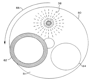
furnished with a lapping plate 50, as shown in Fig. 10.
The lapping plate 50 has a lapping surface 51 made of a
soft metal material. For example, a 15 inch diameter
lapping plate 50 made of a copper composite with polymers
may preferably be used. Such a copper composite lapping
plate is also available from Engis Corp. The flatness of
the lapping plate 50 is preferably determined using a
flatness gauge 52, also available from Engis Corp. The
flatness gauge 52 is preferably calibrated on a flat
granite block. The lapping plate surface 52 is preferably
slightly concave at its center with respect to its outer
edge. Thus, as shown in Fig. 10, the flatness gauge 52
will show a negative reading at an inner position near the ,
lapping plate's center. The concavity of the lapping plate
may preferably be 0.0002 to 0.0005 inches of concavity at ,
the center of the lapping plate 50 with respect to the
outer edge of the lapping plate 50. (The concavity shown
in Fig. 10 is exaggerated for illustration purposes.) It
is important to maintain concavity of the lapping plate 50
CA 02245498 1998-08-OS
~'~VO 97!28925 PCT/LTS97/OIZ66
-28-
so that the lapping plate 50 will have a near perfectly
flat surface 51 (zero mil flatness) when used during the
lapping process. The copper composite material which forms
' the lapping plate 5o undergoes expansion over time. It is
difficult to bring the lapping plate 50 to zero mil
i:latness if it is in a convex position. This, in turn,
will adversely affect the z-dimensional stability of the
lapping process.
The lapping plate 50 is conditioned to form small
ridges of cantrolled height in the lapping surface 51. The
lapping plate 50 may preferably be conditioned using a
diamond conditioning ring 54 as shown in Fig. 21. The
diamond conditioning ring 54 has a surface 56 embedded with
diamonds which form the ridges in the surface 51 of the
lapping plate 50 when the plate 50 is rotated while in
contact with the ring 54. Diamond conditioning rings 54 of
various grits are available from Engis Corp. A course grit
conditioning ring (60-80 grit) is preferably used if the
lapping process is to employ a diamond slurry having
diamond particles greater than 10 ~m in size. Otherwise, a
finer grit diamond conditioning ring (140-170 grit) may be
used. For a copper-composite lapping plate 50, the lapping
plate 50 should preferably always be wet with W-Lubricant
(also available from Engis Corp.) before diamond
conditioning. A typical duration for diamond conditioning
is 2 minutes at &0 rpm rotation of the lapping plate 50,
but will depend on the slurry size used.
Diamond conditioning applies a rough ridged
surface 51 to the lapping plate 50, and may also be used to
obtain the desired concavity of the lapping plate. The
position of the diamond conditioning ring 54 during the
conditioning process may preferably be determined depending
on the initial flatness of the lapping plate 50. The
_ preferred position of the conditioning ring 54 for a
concave lapping plate 50 is shown in Fig. 11. Far a convex
lapping plate 50, as shown in Fig. 12, the flatness gauge
52 will show a positive reading at an inner position of the
lapping plate near the center of the lapping plate 50. The
CA 02245498 1998-08-OS
WO 97/28925 PCT/LJS97/01266
-19-
preferred position of the diamond conditioning ring 54 for
a convex lapping plate 50 is shown in Fig. 13. As shown,
one edge of the conditioning ring 54 is aligned with the
outer edge of the lapping plate 50. Fig. 14 shows a
lapping plate 50 in which the lapping plate surface 51 is
hollow or concave between the outer edge and center of the
lapping plate 50. For such a lapping plate 50, the
flatness gauge 52 will show a negative reading at a center
position between the center and outer edge of the lapping
plate 50. For this type of lapping plate, the preferred
position of the diamond conditioning ring 54 is shown in
Fig. 15. As shown, the diamond conditioning ring 54 is
centered over the concavity in the lapping plate surface
51.
After diamond conditioning, the lapping plate 50
is thoroughly cleaned so that wipes of the lapping plate
surface with a clean cloth do not show any traces of copper
particles remaining on the plate. The flatness of the
lapping plate 50 is then preferably re-measured, using the
flatness gauge 52, and the plate re-conditioned, if
necessary, in order to obtain the desired concavity.
A second conditioning step follows the diamond
conditioning. During this step, as shown in Fig. 16, free
diamond particles in a liquid slurry 58 are sprayed from a
nozzle f0 onto the surface 51 of the lapping plate 50.
Diamond lapping/polishing slurries are available from Engis
Corp. in a wide variety of diamond particle sizes (0.5 um -
gum) suspended in a mineral oil. The diamond particle
size used depends upon the finish of the polished surface
30 and rate of material removal and polishing which are
desired. Diamond size also affects the shear forces which
will be applied to the surface being lapped. During this
second conditioning step, the diamond slurry 58 is sprayed
onto the surface 51 of the lapping plate 50 for preferably
approximately 5 seconds with the plate rotating at
approximately 50 rpm. A clean and dry ceramic conditioning
ring s2 is then placed on the lapping plate 50, at one of
the roller arms on the polishing machine, ahead of the
CA 02245498 1998-08-OS
VhC 97!28925 PCT/US97/0126(
-20-
spray position. The ceramic conditioning ring 62 is
preferably centered over the lapping surface of the lapping
plate 50, as shown. The ceramic conditioning ring 62, also
available from Engis Corp., helps to embed the fine sized
diamonds from the slurry 58 into the lapping plate 50,
specifically, into the ridges formed by the diamond
conditioning ring 54 during the first conditioning step.
This prevents the diamonds from rolling on the lapping
plate surface during the lapping process. With the ceramic
conditioning ring 62 in place, the second conditioning step
may preferably proceed for approximately 1 minute with the
nozzle 60 dispensing the diamond slurry 58 onto the surface
51 of the lapping plate 50 for 3-4 seconds after a 40
second interval. The conditioned lapping plate 50 is now
prepared for lapping a workpiece, such as a substrate wafer
upon which a photoresist-metal layer has been deposited, or
similar microstructure parts.
The workpiece to be lapped is mounted onto the
lapping plate 50 for lapping. A piece to be lapped may,
for example, be mounted on the plate using the vacuum
holddown on an Accupol Vacuum Fixture, from Lapmaster.
This device has a built-in thickness monitoring capability.
The Accupol Vacuum Fixture may be placed on a flat granite
block to zero the thickness monitoring gauge on the
fixture. The electroplated wafer substrate, or other piece
to be lapped, is then mounted on the vacuum chuck of the
fixture, and the fixture is placed on the lapping plate 50
ahead of the ceramic conditioning ring 62. The angle
between the vacuum chuck and the lapping plate surface 51
is preferably as close to 90° as possible. The relative
positions on the lapping plate surface 51 of the diamond
slurry spray 58, ceramic conditioning ring 62, and
workpiece to be lapped 64, with respect to the rotation of
the lapping plate 50, indicated by arrow 66, are as shown
in Fig. 17. Weights are applied to the mounting fixture t:o
bring the contact pressure between the workpiece 64 and the
surface 51 of the plate 50 to a maximum of 5 psi. The
weight to be placed on the micro part being lapped is based
CA 02245498 1998-08-OS
WO 97!28925 PCT/US97IO1Z66
-2 2.-
on the geometry and dimensions of the parts. Small sized
structures (e. g., l0o~m X 100~cm parts, 50~,m high) require
the starting weight to be minimized in order to avoid
adhesion losses due to shear forces. Increased contact
pressure may be required to lap large dimension parts.
Weights, conditioning rings, etc., should not be left on
the lapping plate 50 when it is not in use.
The lapping process may begin by starting
rotation of the lapping plate 50 at, e.g., 25 rpm and
increasing the rotation slowly to 40 rpm. The diamond
slurry 58 is preferably dispensed for 2-3 second periods at
regular intervals of 30-40 seconds. Shear forces applied
to the piece being lapped, and the characteristics of the
surface finish finally achieved, are controlled in part by
the diamond size in the slurry. Larger slurry size results
in larger shear forces and a rougher final finish.
The lapping method and apparatus of the present
invention reduces shear forces by the use of the diamond
slurry 58 in combination with the soft metal lapping plate
50. As lapping proceeds, the diamond particles embedded in
the ridges of the lapping plate 50 will be dislodged from
the lapping plate 50 as shear forces increase, rather than
causing damage to the photoresist or metal layer being
lapped. Thus, lapping of a photoresist-metal layer can be
accomplished without loss of adhesion between the
photoresist-metal layer and the substrate beneath due to
high shear forces. The risk of tearing or shredding of the
photoresist layer surface is similarly reduced.
The lapping plate 50 should periodically be re-
conditioned using the diamond and ceramic conditioning
rings in the manner described above. Re-conditioning
should preferably occur after every 20-30 minutes of
lapping, or when the cutting rate decreases significantly
(by over 50~). The lapping plate 50 is preferably cleaned
with de-ionized Water and a soap solution, and thoroughly
dried, before it is re-conditioned using the diamond and
ceramic conditioning rings and the process described
earlier. Re-conditioning is necessary because, after some
CA 02245498 1998-08-OS
WO 97!28925 PCT/US97l01266
-22-
time, the ridges formed in the surface of the lapping plate
50 during the initial conditioning using the diamond
conditioning ring 54 become worn out.
' The amount of material cut from the piece being
lapped 64 is monitored during the lapping process using the
' thickness gauge on the vacuum fixture. For some
electroplated metals, the lapping process just described
will cause metal from a microstructure to smear into
adjacent photoresist areas. This smearing 68 is
l0 illustrated in Fig. 18 which shows the substrate with
photoresist and metal layer of Fig. 4 after initial lapping
using the method just described. This smearing is
generally not acceptable. Thus, when the structure height
of the workpiece 64 is reduced to within 20-30 microns of
the final desired height, it is preferable that a finish
lapping step be used. The lapping plate 50 is
reconditioned, as described above, and finish lapping
proceeds using a 1 ~m dimond slurry and a moderate contact
pressure weight of 2-3 psi at a rotational speed of 40 RPM
for a prolonged period of time. The finish lapping step
removes an additional 15-25 um of material from the surface
being lapped. This removes any smearing 68 from the
workpiece surface. Finish lapping is preferably
interrupted to inspect the workpiece surface when the
height is within 10 ~m of the final desired height. If
same smearing remains, the weight on the lapping parts may
be increased to increase the contact pressure during the
finish lapping step. At the completion of this step all
electroplated areas on the surface of the workpiece 64
should be in contact with the lapping plate surface 51.
When the desired thickness {structure height) is reached,
the piece 64 is removed from the lapping plate 50. In
order to remove the vacuum fixture from the plate 50, it is
slid radially outward, and never lifted vertically up from
the lapping plate 50.
Once the lapped parts are reduced to within
3-5 ~cm of the final desired height, a polishing step is
preferably used to apply a final smooth finish to the
CA 02245498 1998-08-OS
WO 97128925 PCT/US97/01266
-23-
workpiece surface. This additional polishing step is
accomplished using a hard polishing plate covered by a
polishing cloth. For example, a stainless steel plate with
a surface flatness of 0.0002 inches, covered with a self
adhesive or PSA backed nylon polishing cloth, supplied by
Beuhler Corp., may be used. This cloth covered polishing -
plate is preferably used on a separate polishing or lapping
machine from the lapping machine upon which the initial
diamond lapping steps of the present invention take place.
The polishing cloth is initially saturated with a 1 ~Cm
diamond polishing slurry available from Engis Corp.
Preferably, the workpiece 64 and workpiece holder are
cleaned thoroughly before mounting the workpiece 64 on the
polishing machine. This will prevent any particles from
the Zapping machine from being transferred to the polishing
machine. Use of a separate vacuum holder for each separate
lapping or polishing machine is preferred. Finish
polishing preferably proceeds for approximately 15 minutes
with a polishing plate rotation rate of 80 rpm. Finish
polishing preferably cuts an additional 3-4 ~cm of material
from the surface to be polished. The final polishing step
produces a work piece with a polished mirror-like finish at
the specified structure height.
The lapping and polishing method just described
has been used to re-planarize the surface of photoresist-
metal layers including metal microstructures made of
nickel, nickelJiron, and copper. Surface profilometry of
the lapped and polished samples reveal height variations
within individual microstructure parts of substantially
less than 0.5 ~Cm, and variations of 1-2 ~Cm over an entire
area of 50 X 30 mm. Scanning electron micrographs of the
sample show no smearing of lapped and polished parts.
A variation on the lapping and polishing method
and apparatus of the present invention just described may
be accomplished using a steel or glass mounting plate,
instead of the vacuum fixture, for supporting the workpiece
64 on the lapping plate 50. The mounting plate 70, shown
in Fig. 19, may preferably be made of glass or steel and
CA 02245498 1998-08-OS
1V0 97!28925 PCTIUS97/OI266
-24-
m.ay be approximately 6 inches in diameter, with both
surfaces paralleled and flattened to a tolerance of less
than 5 X 10⁻⁵ inches. The mounting plate 70 is heated to
approximately 55-60°C. A wax, e.g., the low temperature
wax made by Hyprez, and available from Engis Corp., is
melted onto the mounting plate 70. The workpiece 64 is
placed on the center of the mounting plate 70, and is
secured thereto by the hardening of the wax. Glass support
pieces ?2 are also secured to the mounting plate 70 using
the wax. During the time period when the wax is cooling,
some weight may be applied to the plate to assure good
adhesion between the glass support pieces 72 and the
mounting plate 70. The glass support pieces 72 may
preferably be 10 mm x 10 mm, or 20 mm diameter glass
pieces, which are approximately 1500 ~m thick, and arranged
in a hexagon arrangement near the edge of the mounting
plate 70 and surrounding the workpiece 64 mounted in the
center of the mounting plate 70. The glass support pieces
72 are thicker than the heights of any structures plated
onto the workpiece 64 to be polished. This is illustrated
in the cross-sectional view of Fig. 20.
After the lapping plate 50 has been conditioned
using the diamond conditioning ring 54, the ceramic
conditioning ring 62, and the procedure described earlier,
the mounting plate 70 may be positioned on the lapping
plate to begin the lapping process. Weights are placed on
the back of the mounting plate 70 in order to bring the
contact pressure between the glass support pieces 72 and
the polishing surface 51 of the lapping plate 50 to a
maximum of 5 pounds per square inch (psi). The glass
support pieces 72 are then lapped using a 60 rpm plate
. rotation and a 30 um diamond slurry dispensed for 3-4
seconds at approximately 40 second intervals until the
- glass support pieces 72 are reduced to a height
approximately 400 um higher than the final desired height
of the piece being polished. The heights of the glass
support pieces 72 are measured periodically during the
CA 02245498 1998-08-OS
WO 97128925 PCT/LTS97l01266
-25-
lapping process. Lapping should not proceed for more than
ten minutes in one continuous cycle before the heights of
the glass pieces 72 are remeasured. After each
measurement, the positions of the weights placed on the
hack of the mounting plate 70 are adjusted, to adjust the
contact pressure between each glass piece 72 and the
lapping plate 50, to thereby level the thicknesses of the
glass support pieces 72. This is done to minimize the
ultimate height variations across the workpiece 64.
The lapping plate 50 is then re-conditioned using
the diamond conditioning ring 54, ceramic conditioning ring
62, and the conditioning procedure described earlier.
Since a smaller diamond slurry size will now be used for
lapping, a finer grit diamond conditioning ring is
preferably employed during the conditioning process.
Lapping of the glass support pieces 72 and workpiece 64
then proceeds using a 15 ~m diamond slurry, until the
structure being lapped is within 10-15 E,cm of the final
desired height. Once again, the height of the glass
support pieces ?2 is periodically measured, and the
positions of the weights on the mounting plate 70 are
periodically adjusted, to level the heights of the glass
support pieces. At the completion of this phase of the
lapping process, the glass support pieces 72 should have
height variation tolerances within 5 um.
The lapping plate 50 is preferably once again re-
conditioned using the diamond conditioning ring 54, ceramic
conditioning ring 62, and conditioning procedure described
earlier. Since a relatively small diamond slurry size will
be used for the next lapping step, a fine grit diamond
conditioning ring 54 is preferably employed in the
conditioning procedure. Finish lapping of the workpiece 64 ,
may then proceed, using a diamond slurry size of 1 um, for
removing a final 15-20 ~Cm of material from the piece 64.
wring this lapping step, the duration of the slurry
dispensing period is preferably increased to approximately
5 seconds, and the dispensing interval is reduced to
approximately 20 seconds. After the workpiece 64 is
CA 02245498 1998-08-OS
fVO 97128925 PCT/US9710I266
-26-
reduced to its desired height, the mounting plate 70 is
removed from the lapping plate 50. Preferably, a finish
polishing step, using a hard polishing plate covered by a
' polishing cloth saturated with a diamond slurry as
described above, may be used to apply the final mirror-like
finish to the piece being polished. To remove the
workpiece 64 from the mounting plate 70, the mounting plate
is re-heated, and the workpiece 64 slid gently off.
'Prichloroethylene (TCE) may be used to dissolve any
l0 residual wax from the back of the workpiece substrate 64.
The alternative lapping and polishing method and
apparatus just described, using a mounting plate 70 instead
of a vacuum holddown fixture, produces the same desirable
surface ffinish as the lapping and polishing procedure
described earlier. As with the previously described
procedure, the use of a diamond slurry for lapping allows
planarization of photoresist and metal microstructure
layers, while minimizing the risk of loss of adhesion of
the photoresist or metal, and shredding or tearing of the
photoresist, due to the high shear forces present in
previously known cutting and milling processes.
As previously discussed, the lapping and
polishing method and apparatus of the present invention is
well suited for the re-planarization of photoresist-metal
layers needed for the fabrication of precision single level
and multilevel microstructures. The present invention may
also be employed, however, for the planarization and height
reduction of preformed photoresist sheets which are used
either for the formation of metal microstructures, or as
photoresist structures having independent utility. The
.reduced shear forces made possible by the lapping and
, opolishing method and apparatus of the present invention
maces it particularly well suited for the removal of
:material from preformed photoresist sheets, because the
risk of shredding or tearing the photoresist sheet, or of
causing loss of adhesion between photoresist sheets or
between photoresist sheets and substrates of other
:materials, is minimized.
CA 02245498 1998-08-OS
WO 97J28925 PCT/US97/01266
-27-
An exemplary microstructure fabrication process
employing preformed photoresist sheets, in which the
lapping and polishing method and apparatus of the present
invention may be employed, is described with reference to .
Figs. 21-26. Referring to Fig. 21, a relatively thick
(e.g., 1-3 mm) preformed photoresist sheet 100 is exposed -
to X-rays 101 passed through an X-ray mask 102 having X-ray
absorbers 103 thereon in patterns which result in regions
105 in the pre-formed sheet 100 which are sufficiently
exposed to X-rays to be removed by developer, but with the
regions 105 extending only part way through the thickness
of the photoresist sheet 100. The photoresist sheet 100 is
then exposed to a liquid developer which removes the
exposed photoresist to form void regions 106, as shown in
Fig. 22. Another photoresist sheet 108 is formed by a
similar process to have void regions 109 therein. The two
relatively thick photoresist sheets 100 and 108 are then
bonded together at their exposed surfaces in a properly
aligned manner so that the void regions 106 and 109
properly align with each other, as illustrated in Fig. 23.
The layer 10o may then be planarized using the lapping and
polishing method and apparatus of the present invention to
remove photoresist material from the layer 100 and reduce
the layer 100 to a thickness wherein the regions 106 are
fully exposed, as illustrated in Fig. 24. Use of the
lapping and polishing method of the present invention to
reduce the photoresist layer 100 allows the height of the
layer 100 to be controlled within strict tolerances,
produces a mirror-like surface on the photoresist layer
100, and may be accomplished with minimal risk of damage to
the photoresist layer 100. As shown in Fig. 25, a further
photoresist sheet 110, having open regions 111 thereon, may
be formed on the two layers 100 and 108 in an entirely
identical manner employing the lapping and polishing method
of the present invention to reduce the height of the
photoresist sheet 110. After the desired number of layers
are formed in the laminate, the laminate may, if desired,
then be bonded to a substrate 113 which has a surface
CA 02245498 1998-08-OS
'WO 97/28925 PCTJUS97/01266
-28-
thereon appropriate for electrodeposition of a multilevel
metal microstructure, as illustrated in Fig. 26. The now
top layer photoresist sheet 108 may then be reduced in
height using the lapping and polishing method of the
present invention to reduce the thickness of the~sheet 108
- to a thickness which exposes the open regions 109, allowing
electrodeposition of metal into all of the regions 109,
:106, and 111. However, it should be understood that the
:Laminate of layers 108, 100 and 110 of photoresist may
itself have independent utility without being bonded to a
substrate as a mold for electrodeposition. For example,
the open regions 106, 109, and 211 may comprise multiple
:Fluid channels to allow routing of liquids or gasses
through the laminate for use in pressure sensors, alarm
devices, hydraulic or pneumatic actuators, etc. Precise
control of the size of the channels thus formed is achieved
by the lapping and polishing method of the present
invention which allows controlled reduction of the
photoresist sheets of which the laminate is formed to the
desired thicknesses. The smooth mirror-like surfaces
achieved by the polishing method of the present invention
also enhances the ability of multiple photoresist sheets to
be securely adhered together by solvent bonding (using,
e.g., a chemical composite of PMMA). Surface tension
:Forces when using the solvent bonding technique are very
:Large when the surfaces being bonded together are very
smooth.
It is understood that the invention is not
confined to the particular embodiments and exemplary
applications set forth herein as illustrative, but embraces
all such modified forms thereof as come within the scope of
the following claims.
v== t~fd~;l~t,A a ~'(~a.i~:"trs~q~'