Note: Descriptions are shown in the official language in which they were submitted.
CA 02245549 1998-08-04
WO 97/29384 PCT/SE97/00068
-1-
ASSEMBL~Y AND METHOD FOR TESTING
INTEGRATED CIRCUIT DEVICES
° TECHNICAL FIELD OF THE INVENTION
The present invention relates generally to electronic
product testing. More particularly, the present invention
relates to a testing assembly capable of testing and
evaluating an integrated circuit device operable at high
frequencies and having a large number of input and output
terminals.
Test signals are applied, if desired, to each
terminal of the integrated circuit device to permit
testing of the entire integrated circuit device. Test
signals can be applied both to differential terminals, and
to single-ended terminals.
BACKGROUND OF THE INVENTION
The fabrication process by which an integrated
circuit device is formed is a complex process. The
integrated circuit device is fabricated upon a wafer, the
integrated circuit (IC) wafer, and subsequently packaged
into an integrated circuit (IC) package.
Even when the fabrication process is closely
controlled and maintained under strict supervision,
defective integrated circuit wafers are sometimes formed.
And, packaging errors, such as missed connections or
misconnections, can occur during packaging of the
' integrated circuit device. Testing for defects and
packaging errors is therefore required to ensure that a
defective IC package is not used in-an electronic circuit.
CA 02245549 1998-08-04
WO 97129384 PCT/SE97/00068
-2-
On-wafer testing, subsequent to fabrication of the
IC wafer and prior to packaging of the integrated circuit '
device can detect defects on the integrated circuit
device. Testing for packaging errors must necessarily be
performed subsequent to packaging operations. Sometimes,
on-wafer testing is partially or completely deferred, and
testing occurs only after packaging. Such deferral is,
however, at the cost, typically, of the resultant need to
discard an increased number of packaged, integrated
10circuit devices. Defects which would otherwise be
detected on-wafer are detected only after packaging of the
integrated circuit devices.
With the trend towards evermore densely populated
integrated circuit devices having more highly integrated
i5 components operable at higher frequencies of operation,
the problems attendant to the testing of an integrated
circuit wafer or a packaged integrated circuit device
formed therefrom become more complex.
As the integrated circuits have become increasingly
2~ more highly-integrated, boundary scan techniques for
detecting faults have become widely utilized. Standard
methodologies of boundary scan testing have been set
forth. For instance, the Institute of Electrical and
Electronics Engineers (IEEE) standard test access port and
2~ boundary scan architecture, IEEE Standard 1149.1-1990, has
been promulgated to set forth industry-wide standards for
boundary scan testing.
In general, such standards call for the formation of
a test access port (TAP) state machine which allows
30 control and access to a boundary scan architecture. To
implement the boundary scan architecture, the integrated
CA 02245549 1998-08-04
WO 97/29384 PCT/SE97/00068
-3-
circuit device must include the boundary scan cells which
are implemented between component terminals and internal
logic circuitry of the integrated circuit device. The
boundary scan cells are also connected together to form
a shift register path around the periphery of the
integrated circuit device, thus giving rise to the term
boundary scan.
Boundary scan techniques can also be utilized to test
the integrated circuit device while still on-wafer.
I0 Testing of the internal logic of the integrated circuit
device is possible by way of the test port. Boundary scan
functions can be used for the testing of primary inputs
and outputs of the integrated circuit device to achieve
controllability and observability of the chip-interior
side of the input and output terminals.
Conventionally, automatic test equipment (ATE) is
utilized for testing of integrated circuit devices.
Conventional ATE typically includes a "testhead" and a
workstation to provide operator control of the integrated
circuit~device undergoing testing, the "device under test"
(DUT). A fixture is required to interconnect, or
interface, the testing equipment with the integrated
circuit device. Such a fixture is of dimensional, and
other, characteristics corresponding to the particular
integrated circuit device. A probe card having pin
' contactors, or probe "needles", for connecting with
terminals of the integrated circuit device connects the
integrated circuit device with the test resources of the
ATE. The ATE typically utilizes three kinds of test
resources: drivers which drive logic inputs, comparators
CA 02245549 '1998-08-04
WO 97/29384 PCT/SE97/00068
-4-
for interpreting output data, and programmable power
supplies.
As the integrated circuit devices become increasingly
integrated and have increasing numbers of input and output
terminals, commensurate increase in the capacity of ATEs
to test the integrated circuit devices, particularly at
the high frequencies of operation of the integrated
circuits is not practical. Further, differential
terminals are oftentimes utilized in high-speed integrated
circuit devices. Differential terminals are formed of
terminal pairs in which differential signals are offset
in voltage relative to one another, one signal referred
to as the positive signal and the other signal referred
to as the negative signal. An external positive
differential of signals applied to a terminal pair
corresponds to an internal logical "1", an external
negative differential corresponds to an internal logical
"0«. To be able to measure correctly a differential
signal in a non-idealized environment, differential
receivers are required. Existing ATEs include merely
voltage comparators capable of quantizing signals in three
voltage windows relative to a ground potential and are
additionally inadequate to test many integrated circuit
devices for this reason.
Therefore, existing apparatus and methodologies of
testing complex, integrated circuit devices are inadequate
to test properly the integrated circuit devices. And, as
the size, complexity, and operational frequencies of
state-of-the-art, integrated circuit devices continue to
increase, the need for improved manners by which to test
CA 02245549 1998-08-04
WO 97/29384 PCT/SE97/00068
-5-
the integrated circuit devices shall become even more
~ pressing.
Testing apparatus which permits appropriate and
economic testing of such integrated circuit devices,
operable at high frequencies of operation, is therefore
necessary.
It is in light of this background information related
to testing apparatus for testing integrated circuits that
the significant improvements of the present invention have
IO evolved.
SUNINIARY OF THE INVENTION
The present invention advantageously provides a
testing assembly, and an associated method, for testing
an integrated circuit device, once fabricated. Static
testing, both functional and parametric testing, and also
dynamic testing of the circuit device can be performed
through operation of the testing assembly.
Testing of an integrated circuit device having almost
any number of input and output terminals is possible.
Such terminals can be formed of single-ended terminals or
differential terminal pairs, or any combination of such
different types of terminals.
Testing operations canbe performed either on-wafer
or after packaging operations have been performed and the
packaged integrated circuit packages have been created.
When testing operations are performed upon the integrated
circuit packages, connections formed during the packaging
operations can further be tested.
Test signals can be applied to large numbers of
terminals concurrently without the conventional
CA 02245549 1998-08-04
WO 9'7!29384 PCT/SE97/00068
requirement to utilize a large number of channels,
otherwise required to test the integrated circuit devices: '
Additionally, test signals can be applied to an
integrated circuit device to permit dynamic testing of the
S circuit device to provide indications of operability of
the integrated circuit device at high frequencies.
Testing of integrated circuit devices, both while
still on-wafer and subsequent to packaging, can be
economically performed. Integrated circuits determined
to have either defects or connection errors can be marked,
or otherwise set aside, to ensure that such defective
circuit devices are not used in an electronic circuit.
In these and other aspects, therefore, a testing
assembly, and an associated method, tests an integrated
circuit having a plurality of terminals. A voltage signal
generator generates test signals of selected voltage
levels. A signal rain interconnects the voltage signal
generator and at least selected terminals of a first group
of the plurality of terminals of the integrated circuit.
The signal rail concurrently applies the test signals
generated by the voltage signal generator to the selected
terminals. A test signal-response indicator is coupled
to at least selected terminals of a second group of the
plurality of terminals of the integrated circuits. A test
signal-response indicator is coupled to the selected
terminals of the plurality of terminals of the integrated
circuit. The test~signal-response indicator indicates
values of output signals generated at the second group of
terminals responsive to application of the test signals
to the terminals. If the output signals indicated by the
test signal-response indicator are of other than desired
CA 02245549 2002-06-21
7
values, a circuit defect. or connection problem might be the
cause of such indication.
More specifi.cal.ly, the present invention provides a
testing assembly for testing an integrated circuit device
having a plurality of terrn.inals, the testing assembly
comprising a voltage signal generator for generating test
signals of selected voltage levels, a first signal rail
coupled to receive the test signals generated by the
voltage signal generator and positionable to extend along
at least a portion of the integrated circuit device, the
first signal r~~il for conducting the test signals generated
by the voltage signal generator therea:long, and a first
group of impedance elements positioned in series with the
first signal rail, the impedance elements of the first
group of impedance elements corresponding in number with a
first subset of the terminals of the plurality of terminals
of the integrated circuit device, each impedance element of
the first group of impedance elements coupled between the
first signal rail and a terminal of at least first selected
terminals of a first group o.f the plurality of terminals,
thereby to apply the test signals conducted along the first
signal rail to the first selected terminals, each impedance
element of the first group of impedance elements of an
impedance level generally matching impedance levels of at
least portions of the integrated circuit device. The
testing assembly further comprises testing means that is
capable of testing at least one element of the integrated
circuit device, the one element selected from the group
consisting of a receiver, a transmitter, and a termination
unit, and a test signal.-response indicat.orcoupled to
selected terminals of a second group of the plurality of
terminals of the integrated circuit device, the test
signal-response indicator for indicating values of output
signals generated at the terminals responsive to
application of the test signals to the terminals.
CA 02245549 2002-06-21
7a
The present invention also provides, in a method for
dynamic testing of an integrated circuit device having an
internal circuit portion and a plurality of bidirectional
terminals, each bidirectional terminal having a receiver, a
S transmitter, and a pulse-signal comparato.r-receiver, an
improvement of a met:hoc3 for testing dynamic operation of
the internal circuit portion by applying a test pulse
having a first selected xoulse width thereto utilizing a
test signal generator, the test signal generator r_apable of
generating a pulse having no smaller than a second pulse
width, the second pulse width larger than tlhe first pulse
width, the method comprising the steps of generating a
first signal pulse at the test signal generator, the first
signal pulse having a first-signal minimum signal value and
IS first-signal maximum signal value, generating a second
signal pulse at the test signal generator, the second
signal pulse having a second-signal minimum signal, the
second-signal minimum signal value greater than the first-
signal minimum signal value, and a second signal-maximum
signal value, the second-signal maxirnum signal value
greater than the first-signal maximum signal value, the
second signal pulse generated at a selected time delay
relative to generation of the first signal pulse during the
step of generating the first signal pulse, thereby to be
offset in phase relative to the first ;signal pulse,
concurrently applying the first signal pulse and the second
signal pulse to the pulse-signal comparator receiver of the
integrated circuit device, forming a test pulse at the
pulse signal comparator-receiver of the integrated circuit
device responsive to application of the firat and second
signal pulses, respectively, during the step of applying,
the test pulse of a pulse width responsive to the phase by
which the first and second signal pulses, respectively, are
offset from one another, providing the test pulse formed
during the step of forming to the transmitters of the
bidirectional terminals, and observing operation of the
CA 02245549 2002-06-21
7b
integrated circuit device responsive to the test pulse
provided during the step of providing.
The present invention also provides, in a testing
assembly for testing a device under test., the device under
test having a plurality of terminals, the testing assembly
having a plurality of probe elements, each probe element
for contacting with a separate terminal of the plurality of
terminals, an improvement of a contact determiner for
determining electrical contact of each of the probe
elements with each of the at least selected terminals of
the device under test, the contact determiner comprising a
plurality of switch devices, a separate switch device of
the plurality of switch devices associated with each
separate probe element of the testing assembly, each switch
device having a first side and a sE=cond side, a voltage
source coupled in series to the first side of each switch
device of the plurality of switch devices, a plurality of
annunciators, a separate annunciator associated with each
separate terminal of the at least selected terminals of the
device under test and probe element of the testing
assembly, each annunciator coupled to a second side of a
switch device of the plurality of switcku devices associated
with a corresponding one of the at least selected
terminals, and each switch device of the plurality of
switch devices positioned in a closed position when the
probe element associated therewith fails to contact with a
terminal of the plurality of terminals, thereby to power
the annunciator to annunciate lack. of the electrical
contact between the probe element and the terminal.
The present invention also provides a method for
testing an integrated circuit device having a. plurality of
terminals, the method comprising the stet:>s of connecting a
testing assembly to at least a portion of they plurality of
terminals of the integrated circuit device, the integrated
circuit device having a plurality of elements that share
access to either a single terminal or a single set of
CA 02245549 2002-06-21
7c
terminals, disabling at least a first element of the
integrated circuit device, enabling at least a second
element of the integrated circuit: device, testing the
second element of the inte<:lrated circuit device, :reading an
output response of the integrated circuit device, and
terminating the testing of the second element of the
integrated circuit device.
A more complete appreciation of the present invention
and the scope thereof can be obtained from the accompanyin_q
drawings which are briefly summarized below, the following
detailed descr.ipti.on of the presently-preferred embodiments
of the invention, and the appended c.l<~im..
BRIEF DESCRIPTION OF THE DRAWINGS
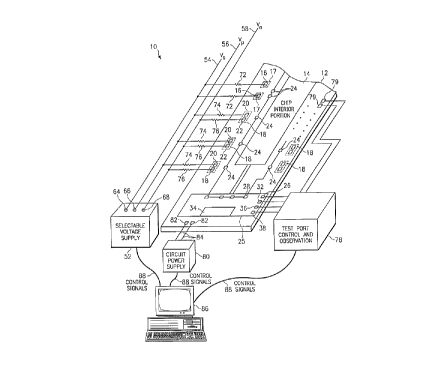
E'igure 1 is a partial, functional block, partial
perspective illustration c>f the testing assembly of an
embodiment of the present invention positioned to test an
exemplary integrated circuit device.
Figure 2 is a simplified circuit schematic of
circuitry including a differential, bi-directional
terminal, exemplary of a terminal fc»~med on the integrated
circuit pictured together with the testing assembly in
Figure 1.
Figure 3 is a flow diagram which lists the steps of a
2~ method of an embodiment of the present invention for
performing static tests upon differential receivers of
bidirectional terminal pairs.
Figure 9 is a flow diagram which lists the steps of a
method of an embodiment of the present invention for
performing static tests upon differential transmitters of
bidirectional terminal pairs.
Figure 5 is a flow diagram which lasts the steps of a
method of an embodiment of the present invention for
performing tests upon built-in differential termination
units of bidirectional terminal pairs.
CA 02245549 1998-08-04
WO 97/29384 PCT/SE97/00068
_g_
Figure 6 is a flow diagram which lists the steps of
a method of an embodiment of the present invention for
performing static tests upon receivers of single-ended
terminals. '
Figure 7 is a flow diagram which lists the steps of
a method of an embodiment of the present invention for
performing static tests upon transmitters of single-ended
terminals.
Figure 8 is a flow diagram which lists the steps of
a method of an embodiment of the present invention for
performing tests upon built-in termination units of
single-ended terminals.
Figure 9 is an illustration of a manner by which
narrow pulses can be formed during operation of an
embodiment of the present invention to permit dynamic
testing of an integrated circuit device.
Figure 10 is a simplified circuit schematic
illustrating portions of the testing apparatus of an
embodiment present invention and portions of an exemplary
integrated circuit undergoing testing by the testing
assembly.
Figure 11 is a flow diagram which lists the method
steps of a method of an embodiment of the present
invention to perform dynamic testing of an integrated
circuit device.
Figure 12 is a circuit schematic of a portion of a
testing assembly of another embodiment of the .present
invention.
Figure 13 is an enlarged view of a single probe
element which forms a portion of the testing assembly
shown in Figure 12.
CA 02245549 1998-08-04
WO 97129384 PCT/SE97/00068
-9-
DETAILED DESCRIPTION
- Referring first to Figure 1, a testing assembly,
shown generally at 10, is positioned together with an
integrated circuit device 12, a portion of which is
illustrated in the figure. The integrated circuit device
12 illustrated in the figure is fabricated as part of an
integrated circuit wafer.
In conventional manner, many integrated circuit
devices are typically fabricated upon a single integrated
circuit wafer. As mentioned previously, once fabricated,
the integrated circuit devices are packaged to form
integrated circuit packages. The testing apparatus 10 is
also operable to test a packaged integrated circuit
package, and tha Packaged-integYatBd circuit package can
l5 instead be illustrated to form the integrated circuit
device 12 in the figure. Additionally, while the testing
assembly l0 is positioned together with only a single
integrated circuit device 12, the testing assembly may
also concurrently test additional numbers of the
integrated circuit devices fabricated upon the wafer.
The portions of the integrated circuit device 12
illustrated in the figure include a chip interior portion
14, typically formed of a large number of circuit
elements. The circuit elements are fabricated and
interconnected to form a desired circuit. The chip
' interior portion 14 is coupled, in conventional manner,
to input and output terminals, here single-ended, bi
directional terminals 16, each forming a cell 17 and
differential, bi-directional terminal pairs 18, each
formed of two terminals 20 and 22. When on-wafer, the
terminals are sometimes referred to as "bond pads", and,
CA 02245549 1998-08-04
WO 97129384 PCTlSE97/OOU68
-10-
once packaged, the terminals analogously are formed as
"pins" or "leads." -
Two single-ended terminals 16 and three differential
pairs of terminals 20 and 22 illustrated in the figure are
merely exemplary of the terminals typically forming
portions ofan integrated circuit device. Typically, an
integrated circuit device includes large numbers of
single-ended or differential terminal pairs, or
combinations thereof.
10As mentioned previously, as integrated circuit
devices increasingly become more complex and include
greater numbers of input and output terminals, use of
conventional testing apparatus to test for proper
operation of the integrated circuit device has become, at
times, impractical. Such conventional, testing apparatus
additionally is typically unable to test properly
differential terminal pairs, or to test circuits which are
operable at high freguencies.
The testing apparatus 10 overcomes the problems
associated with conventional testing apparatus utilized
to test integrated circuits. The apparatus 10 permits the
application of testing signals to an integrated circuit
having even very large numbers of terminals. The
terminals can include single-ended, bi-directional input
and output terminals, differential, bi-directional input
and output terminals, or combinations of such terminals.
And, test signals generated by the testing apparatus can
further be applied to integrated circuit devices to test
their operability at high frequencies.
The integrated circuit of the exemplary integrated
circuit device 12 incorporates the standard, boundary scan
CA 02245549 1998-08-04
WO 97!29384 PCT/SE97/00068
-11-
elements in accordance with the aforementioned IEEE
' Standard 1149.1. The illustrated portion of the
integrated circuit therefore further includes boundary
scan cells 24 associated with each of the single-ended
terminals 16 forming the cells 17 and the terminals 20 and
22 of the differential terminal pairs forming the cells
18. The boundary scan cells 24 are connected together to
form a boundary scan register.
The boundary scan register formed of the boundary
scan cells 24 is coupled to additional on-chip test logic
25, conventional of boundary scan circuitry here including
the elements pictured in the block. A test data input
(TDI) 26 and an instruction register 28 form portions of
the test logic 25. A test data output (TDO) 32 is also
coupled to the boundary scan register and the instruction
register.
A test access port (TAP) controller 34, functionally
operative as a state machine, is further pictured to
receive inputs supplied at a test clock (TCK) terminal 36
and to a test mode select (TMS) terminal 38.
Additional details relating to, and describing
operation of, the boundary scan architecture can be found
in the aforementioned IEEE Standard.
The testing assembly 10 includes a selectable voltage
supply 52 operable to generate test signals of selected
voltage levels. The test signals are generated on supply
rails 54, 56, and 58 which are coupled to the voltage
supply 52 by way of output ports 64, 66, and 68,
respectively, of the voltage supply.
3d The supply rail 54 contacts with the single-ended
terminals 16 forming the cells 17 through resistors 72,
CA 02245549 1998-08-04
WO 97/29384 PCT/SE97/00068
-12-
the supply rail 56 contacts with the terminals 20 of the
terminal pairs forming the cells 18 through resistors 74,
and the supply rail 58 contacts with the terminals 22 of
the terminal pairs forming the cells 18 throughresistors
76. The resistors 72, 74, and 76 are each of impedance
values which match closely the signaling environment in
which the device under test is constructed to operate.
While, for purposes of illustration, only the
terminals formed at the left-hand side (as-shown) of the
portion of the integrated circuit device are shown in the
figure, the supply rails can similarly be positioned to
permit contact with additional terminals of the device,
typically positioned near additional edge surfaces, or
elsewhere, of the integrated circuit device.
The test signals formed at the output port 64 are of
selected voltage levels V8 which may be of selected
sequences of voltage levels, as shall be described in
greater detail below. Test signals of voltage levels Vp
are formed at the output port 66 of the voltage supply,
and test signals of voltage levels Vn are formed at the
output part 68 of the voltage supply. The voltage levels
of the test signals are generated to be of values, e.g.,
to function as a stimulus to receivers, to function as
load voltages for transmitters, and to function as a
stimulus and/or load voltage for built-in terminations.
Such receivers, transmitters and built-in terminations
form portions of the cells 17 and 18, as shall be noted
below.
The testing assembly 10 further includes an observer
3(! and controller 78 which contacts with the test logic 25.
Values of the boundary scan cells loaded into the test
CA 02245549 1998-08-04
WO 97!29384 PCT/SE97/00068
-13-
logic 25 responsive to generation and application of the
- test signals to the integrated circuit device 12 are
observed by the controller 78. If the values observed by
the controller 78 are other than desired values, a defect
of the integrated circuit device 12 might exist. The
observer and controller 78 can also be utilized for
additional functions, inter alia, to test unidirectional
terminals in conventional manner.
During operation of the testing assembly 10, test
signals are generated. The test signals are applied to
the terminals 16, 20 and 22. The values of the boundary
scan cells are loaded into the test logic, and a
determination can be made of the operability of the
integrated circuit device 12 responsive to the
observations of the test port observer and controller 78.
The illustrated portion of the integrated circuit
further includes terminals 79, here coupled to receive
signals generated by the controller and observer 78. As
shall be described in detail with respect to Figure 9
below, the terminals 79 extend to uni-directional
receivers which form portions of the integrated circuit.
The testing assembly 10 further includes a plurality
of power supplies, of which the circuit power supply 80
is exemplary. The power supply 80 supplies operative
power to the power contacts 82 formed on the integrated
' circuit device 12 by way of lines 84. Each power supply
can also have multiple numbers of contacts.
The selectable voltage supply 52, the test port
observer and controller 78, and the power supply 80 are
coupled to an exemplary work station 86 by way of cables
88. Control signals generated at the work station are
CA 02245549 1998-08-04
WO 97129384 PCT/SE97/00068
-14-
transmitted upon the cables 88 to control operation of
such devices, and signals generated at such devices can
also be supplied to the workstation thereby.
Figure 2 illustrates an exemplary, differential
S terminal pair forming a cell 18 together with additional
circuitry which forms a portion of the integrated circuit
of the integrated circuit device 12 shown in Figure 1.
The terminal pair forming the cell 18 includes a positive
terminal 20 and a negative terminal 22 formed upon, or
otherwise accessible at, a surface of the integrated
circuit device 12.
The positive terminal pad 20 is coupled to an input
terminal of an amplifier forming a receiver 96 and to an
output of an amplifier forming a transmitter 98, through
a resistor 102. Analogously, the negative terminal 22 is
coupled to a negative input of the receiver 96 and to a
negative output of the transmitter 98 through the resistor
104. ° The resistors 102 and 104 are of impedances
designated by RD.
Differential inputs received at the terminal pads 20
and 22 are applied to the receiver 96, and internally-
generated output signals applied to the transmitter 98 on
line 106 are supplied to the terminal pads 20 and 22.
The terminal pair forming the cell 18 is also
illustrated to include a built-in termination unit 108
formed of a positive termination resistor 112 and negative
termination resistor 114. The resistor 112 is coupled
between the terminal pad 20 and a signal ground, and the
resistor 114 is coupled between the terminal pad 22 and
the signal ground.
CA 02245549 1998-08-04
WO 97129384 PCT/SE97/00068
-15-
A switch element 116 includes switches 117A and 117B
positioned in-line between the terminal pads 20 and 22 and
the termination resistors 112 and 114-, respectively.
Positioning of the switches of the switch element 116
in the illustrated embodiment is controlled by the
boundary scan cells, here a flip-flop 118 thereof,
connection thereto represented by the line 120. The
boundary scan cells are similarly coupled, here by a flip-
flop 122 thereof, to the enable control input of the
transmitter 98, such connection indicated by the line 124
extending between the flip-flop 122 and the transmitter
98. The boundary scan cells are further similarly
coupled, here by a flip-flop 126 thereof, to the receiver,
such connection indicated by the line 127 extending
IS between the flip-flop 126 and the enable control input of
the receiver 96. The flip-flops 118, 122, and 126 may,
e.g_, alternately be formed of a mode register of test
logic.
Boundary scan cells 128 and 129 are further
illustrated in the figure. The cell 128 is coupled to
line 106 through a multiplexer 130 to the transmitter 98,
and the cell 129 is coupled to the output of the receiver
96. Line 131 forms a second input to the multiplexer 130.
As shall be described with respect to Figure 9 below,
narrow pulses are generated on the line 131 when
performing dynamic testing of the integrated circuit
device. Both. cells 128 and 129 are coupled to core
circuit logic of the chip interior portion 14 (shown in
Figure 1).
Figure 2 further illustrates a built-in high-speed
pulse detector 132 formed of the elements positioned
CA 02245549 .1998-08-04
WO 97/29384 PCT/SE97/00068
-16-
within the block, shown in dash, in the figure_ More
particularly, the pulse detector 132 includes a pair of '
flip-flops 133 and 134. The flip-flop 133 is coupled to
the receiver 96 and also to receive a fixed signal, here
a logical "one" generated by another portion (not shown)
of the circuit undergoing tests. The signal of the
logical "one" value is here, representative of a "passed"
test . < An output of the flip-flop 133 is coupled to an
input of the flip-flop 134. An output of the flip-flop
134 is also provided to a reset input of the flip-flop
133. Operation of the pulse detector 132 shall be
described more fully with respect to Figures 10-11 below.
Once the testing assembly 10 is positioned to contact
the terminals of the integrated circuit device 12 which
is to undergo testing, test procedures can be performed
to test the operation of the integrated circuit device.
In one embodiment, static tests are performed upon the
terminals first to determine the functionality of the
integrated circuit devices and then, if the circuit is
2~ determined to be functional, to determine the parameters
of operation of the device viz., parametric testing of the
circuit is performed to determine if the integrated
circuit meets parametric specifications. And, dynamic
testing of the integrated circuit device is performed to
determine whether the integrated circuit device is
operable at desired frequencies of operation.
While not separately shown, it should, of course, be
understood that a single-ended terminal pair could
similarly be illustrated together with the. additional
circuitry shown in Figure 2_
CA 02245549 1998-08-04
WO 97129384 PCT/SE97/00068
-17-
Figure 3 illustrates the method steps of a method,
- shown generally at 135, for performing static tests upon
the differential receivers, of which the receiver 96 of
the terminal pair 18, shown in Figure 2 is exemplary. The
static tests are performed upon the differential receivers
to determine their functionality and the parameters of
their operation. First, and as indicated by the block
13&, the differential transmitters, such as the
transmitter 98 shown in Figure 1, are disabled, for
example, by way of the test port of the tap machine 34.
The built-in termination units, such as the built-in
termination unit 108 are disabled, as indicated by the
block 137. Disabling of the transmitters by way of, e.g.,
line 124 and termination units by way of, e.g., line 120
can also occur concurrently or in reverse order.
Thereafter, and as indicated by the block 138, the
receivers are tested to determine their sensitivity and
common mode range. Such. testing can be performed, for
example, by applying, in an iterative procedure together
with blocks 140 and 141 noted below, minimum positive and
negative differential voltages at the extremes of the
common mode range on the positive and negative supply
rails 56 and 58, respectively, such rails forming portions
of the testing assembly 10 shown in Figure 1.
Responses formed by the receivers can be read, as
indicated by block 140, via the boundary scan cells by,
for example, a test port observer and controller 78
forming the portion of the assembly ZO of Figure 1. Then,
and as indicated by the decision block 141, a
determination is made as to whether further testing is
required. If so, i.e., if the iterative procedure is
CA 02245549 1998-08-04
WO 97129384 PCT/SE97/00068
-18-
completed, the yes branch is taken back to block 138.
Otherwise the no branch is taken to block 142 and the
receiver test is terminated.
Static tests can analogously be performed upon the
differential transmitters of the differential terminals.
Figure 4 illustrates a method, shown generally at 143,
listing the method steps of a method for performing static
tests upon differential transceivers. First, and as
indicated by the block 144, the differential transmitters,
such as the transmitter 98 shown in Figure 2, are enabled.
The transmitters are enabled, for instance, by way of the
test port of the boundary scan circuitry, as above
described. In the exemplary terminal pair illustrated in
Figure 2, the transmitter 98 thereof is enabled responsive
to appropriate input on line 124. Then, and as
indicated by the block 146, the differential receivers,
of which the receiver 96 shown in Figure 2 is exemplary,
are enabled. And, as indicated by the block 147, the
built-in termination devices are disabled_ Again, other
orders of sequences, or concurrent enabling and disabling
is possible. In the terminal pair 18 illustrated in
Figure 2, the switches 117 and 117B of the switch element
116 are opened, responsive to appropriate commands
generated on the line 120.
Thereafter, the transmitters are tested for level and
drive strength of both pullup and pulldown circuitry on
both their positive and negative outputs, as indicated by
the block 148. With reference back to Figure 2, a logical
"1" stored at the cell 128 activates the positive pullup
and negative pulldown. Analogously, a logical "0" stored
at the cell 128 activates pulldown on positive and pullup
CA 02245549 1998-08-04
WO 97/Z9384 PCT/SE97/00068
-19-
on negative. When testing the transmitters with the
testing apparatus, for instance, the voltage levels of the
test signal generated on the supply rail 58 is first
caused to be of a low voltage level and the voltage level
of the test signal generated on the supply rail 56 is
generated at two different levels. The response to such
different signal levels is observed. after each test
step, the circuit response is read, as indicated by block
149.
By generating test signals on the supply rail 56 of
a low value, and by generating test signals on the supply
rail 58 of two different values, circuit pullup on
negative output of the transmitter are tested.
In analogous manners, the circuit can be tested for
pulldown responses for both positive and negative outputs.
To test for circuit pulldown response on positive outputs,
the test signals generated on the supply rail 58 are
selected to be of high voltage levels and the test
signals generated on the supply rail 56 are selected to
be two separate values, and the receiver response to such
differing levels is observed.
To test for pulldown response of the circuit
responsive to a negative output, the test signals
generated on the supply rail 56 are set at high voltage
levels, and the test signals generated on the supply rail
' 58 are selected to be of two different values. The
receiver response is then observed.
As indicated by the decision block 151, a
determination is made as to whether further testing is
required. If so, the yes branch is taken back to block
148. Otherwise the no branch is taken to block 152 and
CA 02245549 1998-08-04
WO 97/29384 PCT/SE97/00068
-20-
the transmitter test is terminated. Individual ones of
the above-noted tests can be performed, and when no
further testing is required transmitter testing is
terminated.
Figure 5 illustrates a method, shown generally at
153, for testing the built-in termination units, such as
the unit 108 shown in Figure 2, according to an embodiment
of the present invention. First, the built-in termination
units are enabled, as indicated by the block 154. In the
IO terminal pair 18 shown in Figure 2, the built-in
termination unit 108 is enabled by closing the switch
elements 117A and 117B by way of appropriate input on the
line 120. As indicated by the block 156, the receivers
are enabled. And, as indicated by the block 158, the
differential transmitters are disabled, for example, by
way of the boundary scan circuitry. Again concurrent
enabling and disabling or other sequences are possible.
The termination units are then, as indicated by the
block 160, tested for impedance matching. With respect
to the testing apparatus 10 shown in Figure 1, test
signals are generated on the supply rails 56 and 58. The
voltage level of the test signal generated on the supply
rail 58 is first set to be slightly higher than the
voltage level of the test signal generated on the supply
rail 56.
Then, the voltage level of the test signal generated
on the supply rail 58 is set to be somewhat less than the
voltage level of the test signal generated on the supply
rail 56. Such test can be repeated at several different
voltage levels, thereby to determine the impedance
matching of the resistors of the built-in termination unit
CA 02245549 1998-08-04
WO 97/29384 PCT/SE9?/00068
-21-
as a function of voltage level. After each of such test
steps, the circuit response is read, as indicated by block
161. Then a determination is made, as indicated by the
decision block 162, as to whether additional impedance
matching testing is required. If so, the yes branch is
taken back to block 160. Otherwise, the no branch is
taken to block 164.
As indicated by the block 164, the differential
transmitters are enabled, again, for example, by way of
the boundary scan circuitry. Then, and as indicated by
the block 166, the impedance characteristic of the
termination unit is tested. The transmitter outputs are
set to generate high output signal levels and the test
signal generated on the supply rail 58 is selected to be
of two separate values. The termination unit impedance
is determined as a function of voltage level.
As indicated by the decision block 168, a
determination is made as to whether further impedance
testing is required. If so, the yes branch is taken back
to block 166. Otherwise the no branch is taken to block
169 and the testing is terminated. The testing process
can thereby be iteratively performed.
Figure 6 illustrates a method, shown generally at
173, for performing static tests upon single-ended
receivers. First, and as indicated by the block 174, the
transmitters are disabled, for example, by way of the
boundary scan circuitry. Then, the built-in termination
units, on terminals including such units, are disabled,
as indicated by the block 176.
Then, as indicated by the block 178, the receivers
of the single-ended terminals are tested to determine
CA 02245549 1998-08-04
WO 97/29384 PCT/SE97/00068
-22-
their gain and offsets from nominal trigger points. With
respect to the testing assembly 10 shown in. Figure 1, test '
signals are generated on the supply rail 54. The test
signals are formed of high and low voltage levels. Then,
as indicated by the block 180, the receiver responsive to
each input voltage value of the test signal is observed
by the test port observer and controller 78. Thereafter,
a determination is made at decision block 181 a to whether
further testing is required. If so, the yes branch is
taken back to block 178. Otherwise, the no branch is
taken to block 182, and testing is terminated.
Figure 7 illustrates a method, shown generally at
183, for performing static tests on single-ended
transmitters. First, and as indicated by the block 184,
the transmitters and receivers of the single-ended
terminals are enabled. Then, and as indicated by the
block 186, the built-in termination units are disabled.
Then, the transmitters are tested to ensure the
functionality of their level and drive strength pullups
and pulldowns, as indicated by the block 188. Pullups and
pulldowns are activated in manners analogous to those
described with respect to method block 148 shown in the
flow diagram of Figure 4, pertaining to the positive
terminals of the terminal pairs. In one embodiment, four
tests are performed upon the circuit. The single-ended
transmitter pullup capabilities are tested in a two-pass
procedure in which the test signal generated an the supply
rail 54 is selected to be of two different values. The
receiver responses of the terminals are observed. The
single-ended transmitter pulldown capabilities are
CA 02245549 1998-08-04
WO 97/29384 PCT/SE97/00068
-23-
similarly tested. After each test sequence, the circuit
response is read, as indicated by block 189.
Then, and as indicated by the decision block 190, a
determination is made as to whether further testing is
required. If so, the yes branch is taken to block 188.
Otherwise, the no branch is taken to block 191 and the
transmitter test is terminated. Iterative execution of
the above-listed test procedures can thereby be performed.
Figure 8 illustrates a method, shown generally at
193, of a method for testing built-in termination units
of single-ended terminals. The termination units of the
single-ended terminals are analogous to the termination
units of the terminal pair 18 shown in Figure 2.
,_ , , ,__ ,_, ,_ ,__ ,____,
FlrSt, and a5 .1IIG11~c~teQ ~7y tFle 1J10CK 194, t.Cle .p1111t-
in termination units are enabled. And, as indicated by
the block 196, the receivers of the single-ended terminals
are enabled. Then, and as indicated by the block 198, the
single-ended transmitters of the single-ended terminals
are disabled.
The impedances of the termination units are then
tested, as indicated by the block 199. Again, the testing
can be performed in a two-pass process wherein the voltage
levels of the test signals generated on the supply rail
54 are of two different values, and the responses of the
receivers of the terminals are observed, as indicated by
the block 200.
As indicated by decision block 201, a determination
is made as to whether further testing is required. If so,
the yes branch is taken back to block 199. Otherwise, the
no branch is taken to block 202 and the testing is
CA 02245549 1998-08-04
WO 97/29384 PCT/SE97/OOU68
-24-
terminated. The mufti-step testing procedure above-
described can thereby be iteratively performed.
Operation of the testing apparatus l0 further permits
dynamic testing of an integrated circuit device, such as
the device 12 shown in Figure 1.
Figure 9 illustrates a manner by which narrow pulses
can be generated during operation of an embodiment of the
present invention. The pulses are utilized to perform
dynamic testing of the circuit device undergoing tests.
As mentioned previously, state-of-the-art, integrated
circuits are constructed to be operable at increased
frequency levels. Existing testing circuitry is unable
to generate test signals to perform dynamic testing of
such circuits. Figure 9 illustrates a manner by which
IS test pulses can be created of pulse widths of small time
duration (i.e., narrow pulse widths).
The pulses so-generated can be utilized for purposes
of dynamic testing of the integrated circuit device
undergoing tests. Signals of characteristics
corresponding to those of waveforms 202 and 204 are
generated by the observer and controller 78 (shown in
Figure 1) and applied to the terminals 79. The terminals
79 form inputs of a receiver portion 206 of a uni-
directional terminal.
The signals 202 and 204 are slightly out-of-phase
with one another, and the value of the signal 204 is less
than the value of the signal 202 at all times but for when
the signal 204 changes state from a low value to a high
value prior to the time at which the signal 202 changes
from a low value to a high value.
CA 02245549 1998-08-04
WO 97/29384 PCT/SE97/OOObB
-25-
The receiver 206 is operative as a differential
comparator and generates a positive-valued output pulse
when the value of the signal 204 is greater than the value
of the signal 202 and returns to a low logical value at
other times, thereby to form pulse 208. The phase
difference between the signals 202 and 204 is
determinative of the pulse width of the pulse 208. By
proper selection of the phase difference, the pulse 208
generated by the receiver 206 is caused to be of
characteristics which can be used for dynamic testing of
the integrated circuit device undergoing testing. The
pulses, such as pulse 208, generated by the receiver 206
can be applied to other circuit elements of the integrated
circuit device undergoing testing, 'thereby to dynamically
test the operation of such circuitry.
High-frequency signals are not required to be
generated externally by the tester apparatus as long as
signals are maintained in a desired phase relationship to
one another in a manner analogous to the relationship of
the signals 202 and 204 illustrated in Figure 9.
Figure 10 illustrates portions of the testing
apparatus i0 and the integrated circuit device 12 shown
previously in Figure 1. The supply rails 56 and 58 and
resistors 74 and 76 of the testing apparatus 10 are again
shown. During dynamic testing, the supply rails are set
' to appropriate signal ground voltage levels. Portions of
a terminal pair 18 are similarly again shown to include
terminals 20 and 22, a receiver 96, and a transmitter 98.
The transmitter 98 is coupled to receive narrow
pulses, such as the narrow pulse 208 generated as
described with respect to Figure 9 above. The built-in
CA 02245549 1998-08-04
WO 97/29384 PCT/SE97/00068
-26-
high speed pulse detector 132 is also again illustrated
in the figure. As noted previously the pulse detector '
132 includes a pair of flip-flops 133 and 134. As further
noted previously, the flip-flop 133 is coupled to the
receiver 96 and also to receive a fixed signal, here a
logical "one" generated by another portion (not shown) of
the circuit undergoing tests. The signal of the logical
"one" value is here, representative of a "passed" test.
An output of the flip-flop 133 is coupled to an input of
10the flip-flop 134. An output of the flip-flop 134 is also
provided to a reset input of the flip-flop 133. Pulses
can be applied to single-ended -terminals in manners
analogous to their application to the differential
terminals described with respect to Figure 10.
Figure 11 illustrates the method steps of a method,
shown generally at 222, for performing a high-speed,
dynamic test of an integrated circuit device utilizing the
narrow pulses, such as the pulse 208 described above.
First, and as indicated by block 224, the built-in
termination devices are disabled. Then, and as indicated
by the block 226, the pulse detectors, such as the pulse
detector 212, are cleared by scanning a logical "one"
through the boundary scan cells of the boundary scan
circuitry of the integrated circuit.
Then, and as indicated by the block 228 , the pulse
detectors are "armed" by scanning a logical-value "zero"
into the flip-flop 216. Then, and as indicated by the
block 232, signals, such as the signals 202 and 204 are
generated and applied to a receiver, such as the receiver
206 shown in Figure 9, thereby to form a test pulse.
Then; and as indicated by the block 234, results of the
CA 02245549 1998-08-04
WO 97/29384 PCT/SE97/00068
-27-
test can be determined by evaluating the values of the
- boundary scan circuitry.
Figures 12 and 13 illustrate a portion of the testing
' assembly 10 of a further embodiment of the present
invention. For the integrated circuit device undergoing
testing to be tested properly, contact must be made by the
testing apparatus with the terminals of the integrated
circuit device undergoing testing. If contact is not
appropriately made, the testing operations are likely to
IO be inadequate. Therefore, it is important to ensure that
the testing apparatus contacts with all of the terminals
of the integrated circuit.
The circuitry illustrated in Figures 12 and 13,
referred to generally at 238, provides an indication of
contact between the testing apparatus and the terminals
of the integrated circuit device undergoing testing. The
circuitry 238 is exemplary of the circuitry which provides
indications of contact of the various bidirectional
portions of the device undergoing testing. Here, the
circuitry 238 is shown to test the contact of the testing
apparatus to three exemplary terminals 16, 20, and 22 of
the integrated circuit device undergoing testing. Such
circuitry is duplicated for each terminal 16, 20, and 22,
as appropriate, of the integrated circuit device
undergoing testing.
' , The signal rails 54, 56, and 58 are again shown to
extend to terminals 16, 20, and 22 through resistors 72,
74, and 76, respectively, as previously shown in Figure
1. The resistors 72, 74, and 76 are preferably of low
impedance values to permit operation of the circuit with
low levels of current drain. The circuitry 238 here is
CA 02245549 1998-08-04
WO 97/29384 PCT/SE97/00068
-28-
shown to include a contact-check reference voltage line
240 upon which a reference voltage is generated. A
transistor 244 is associated with each of the terminals
16, 20, and 22. A gate electrode of each of the
transistors 244 is coupled to an appropriate one of the
signal rails 54, 56, or 58. Remaining electrodes of the
transistors 244 are coupled between the voltage line 240
and light emitting diodes 246. The diodes 246 are coupled
to an offset potential (e. g., a ground potential? through
resistor 248. If adequate contact with any of the
terminals 16, 20, and 22 is not formed, the transistor 244
associated with such terminal turns-on, the diode 246
associated therewith turns-on, and a signal is generated
on line 247. Line 247 is coupled to a bad contact alarm
250, and appropriate annunciation is made.
The voltage levels of the supply rails 54, 56, and
58 and of the line 240 are selected such that, when the
contact is made with a terminal 16, 20, or 22, as
relevant, the voltage drop across the corresponding one
20of the resistors 72, 74, or 76 causes the voltage
differential between the line 240 and the gate electrode
not to be great enough to turn the transistor on.
Conversely, if the proper contact is not made with the
terminal, the voltage differential between the gate
electrode of the associated transistor and the line 240
is great enough to turn the transistor on, and power the
associated diode 246. While the illustrated embodiment
utilizes p-channel MOSFET transistors 244, other
transistors can, of course, instead be utilized with
30appropriate changes in biasing voltages on the lines 54,
56, and 58, as appropriate.
CA 02245549 1998-08-04
WO 97/29384 PCT/SE97/00068
-29-
During initial positioning of the testing apparatus
together with an integrated circuit device, the signal
generated on line 247 can be used in a feedback control
arrangement to determine when the testing apparatus is
S properly positioned. Lighting of the diodes 246
facilitates troubleshooting operations, if necessitated,
to complete the proper contacting of the testing apparatus
with the integrated circuit undergoing testing.
Figure 13 illustrates an exemplary physical
10 arrangement of contact detecting circuitry for probe card
fixturing of a device under test which forms a portion of
the testing assembly I0 including the circuitry 238 shown
in Figure 12. The small distance separating the resistor
and the probe tip is shown in Figure 13. Such small
distance facilitates high-speed, i.e., dynamic testing
operations. Inadequate connections between the testing
assembly and terminals of the integrated circuit
undergoing testing are detected and indicated so that
appropriate correction of the connection can be
effectuated. While the physical arrangement of the
circuitry 238 utilized in the testing of a packaged
integrated circuit is not separately shown, the
arrangement is similar but for the positioning of the
transistors 244 thereof.
Operation of various of the embodiments of the
present invention permits an integrated circuit device
having almost any number of input and output terminals to
be tested. Static testing, both functional and parametric
testing, and also dynamic testing of the circuit device
can be performed.
CA 02245549 1998-08-04
WO 97/29384 PCT/SE97/00068
-30-
The integrated circuit device undergoing testing can
.include single-ended terminals or differential terminal '
pairs, or any combination of such different types of
terminals. '
Testing operations can be performed either on-wafer
or after packaging operations have been performed and the
packaged integrated circuit packages have been created.
When testing operations are performed upon the integrated
circuit packages, connections formed during the packaging
operations can further be tested.
Test signals can be also be applied to an integrated
circuit device to permit dynamic testing of the circuit
device to provide indications of operability of the
integrated circuit device at high frequencies. Testing
of integrated circuit devices, both while still on-wafer
and subsequent to packaging, can be economically
performed. Integrated circuits determined to have defects
found to have either defects or connection errors can be
marked, or otherwise set aside, to ensure that such
defective circuit devices are not used in an electronic
circuit.
The previous descriptions are of preferred examples
for implementing the invention, and the scope of the
invention should not necessarily be limited by this
description. The scope of the present invention is
defined by the following claims.