Note: Descriptions are shown in the official language in which they were submitted.
CA 02245567 1998-08-04
WO 97/28611 PCT/US97/01996
TITLE
Synchronization and downconversion in TDM/TDMA systems
Field Of The Invention
The present invention relates to a method and apparatus
for the synchronization of the data in a telecommunications
system and downconversion of data modulated onto a radio
frequency carrier.
Background Of The Invention
In the area of telecommunications, there have been
advances in Fiber-to-the-Curb (FTTC) technology in which
devices in the home are connected to the telephone central
office via a network of one or more optical fibers
connecting the central office to network points called
Broadband Network Units (BNUs) which in turn connect to the
subscriber home via a coaxial cable, and to the devices in
the home via a passive splitter and in-home coaxial wiring.
In these FTTC networks, signals can be routed to the home
via a single coaxial cable connecting the home to the BNU.
Using the FTTC configuration with a coaxial drop cable,
devices in the home including telephones, computers and
televisions will be connected to the coaxial network.
Because there are multiple devices in the home which will
all transmit back to a central receiver, and because
telecommunications services require accurate clocks for data
recovery and transmission, it is important to have a method
of synchronization which allows the devices in the home to
recover an accurate system clock, and to transmit and
receive on the correct frequencies and at the correct data
rates.
In addition to the above mentioned problem, there are
multiple devices in the home which are connected to the BNU
on a single coaxial cable, a multiple access protocol such
as Time Division Multiple Access, Code Division Multiple
Access, or Frequency Division Multiple Access is used to
CA 02245567 1998-08-04
WO 97/28611 PCT/US97/01996
access the BNU from the devices in the homes. These
multiple access protocols typically require an accurate bit
clock as well as an accurate carrier frequency.
When data is received at the BNU, it is necessary to
process the signal, which is typically a radio frequency
signal, and recover the information transmitted from the
devices. A first step in recovering the information is
downconversion, in which the radio frequency signal is
shifted in frequency to a baseband signal. This process can
be complex and can require an excessive amount--of signal
processing power due to the high data rates and the high
speed sampling required to digitize the radio frequency
signal.
Another difficulty which is encountered in such a
system is the fact that other services such as traditional
cable TV may be provided on the same coaxial drop cable, and
thus it is important to select frequencies for both
downstream (BNU-device) and upstream (device-BNU)
transmission which do not interfere with the cable TV
services which are typically in the 50-750 MHz frequency
range.
For the aforementioned reasons there is a need for an
accurate, low cost method of synchronization in a FTTC
system which employs a coaxial drop to the home, and to
select frequencies for downstream and upstream transmission
which permit use of the coaxial cable for the transport of
other services at other frequencies. It is also necessary to
have an efficient method of downconversion.
Summary Of The Invention
In a FTTC system transmission of downstream data from a
BNU to devices in a residence is accomplished by
transmitting downstream data on a downstream radio frequency
(RF) carrier in which both the downstream data rate and
2.
CA 02245567 1998-08-04
WO 97/28611 PCT/US97/01996
downstream RF carrier are integer multiples of a sub-
harmonic of a master clock.
Data from devices in the residence is transmitted to
the BNU on an upstream RF carrier, and both the upstream RF
' S carrier and upstream data rate are integer multiples of a
sub-harmonic of a master clock.
In one embodiment, a 155.52 Mb/s data signal is
received at the BNU over an optical fiber and within the BIU
(in the BNU) the clock recovered from this signal serves as
a reference clock, from which a 19.44 MHz clock (1/8 of the
155 Mb/s clock signal) is produced. A local oscillator at
622.08 MHz is locked to the 19.44 MHz clock. The 622.08 MHz
clock serves as a carrier for the downstream data, which has
a data rate of 51.84 Mb/s. A 51.84 MHz clock can be easily
derived from the 155.52 MHz clock. A 38.88 MHz receive clock
is also generated at the BIU, based on locking to the 19.44
MHz clock.
At the NIM (in the device in the home) the 622.08 MHz
carrier is recovered, as is the 51.84 MHz bit clock.
Because these two signals are synchronous, a number of
methods can be used to derive them. A 19.44 MHz clock,
?7.76 MHz clock, and 38.88 MHz clock can all be readily
generated, since the system is synchronous and all of the
frequencies are harmonically related. Upstream transmission
to the BIU can take place at a carrier frequency of 38.88
MHz, with a data rate of -19.44 Mb/s.
In an alternate embodiment, the downstream transmission
takes place at a carrier frequency of 19.44 MHz, with a data
rate of 51.84 Mb/s. This embodiment has the advantage of
not disrupting the spectrum above 550 MHz, thus leaving all
of that spectrum available for cable TV or other
applications.
A method of digital downconversion is used for
reception of upstream data in the BNU in which a baseband
signal is generated by a downconversion process in which the
first step is sampling of the RF passband signal at a rate
3.
CA 02245567 2002-06-18
which i~ equal to 4/3 the upstream,carrier freguency.
Subsequent to this sampling, a baseband signal is generated
by multiplication of the sampled bandpass signal by e-~~,
where n represents a discrete time variable. The complex
baseband signal is separated into a real and imaginary part
to create the I and Q channels. The resulting baseband
signals, one for the I channel and one for the Q channel,
are interpolated to produce three output samples for every
input sample. Low pass filtering is performed on the
interpolated signals, and the resulting filtered baseband
signals are decimated by eight to produce one output sample
for every eight input samples.
An advantage of the present invention is that a minimum
of phase-locked-loops are required, and that downconversion
can be accomplished in a cost effective manner on a silicon
integrated circuit, since many of the multiply operations in
the digital signal processing steps can be eliminated.
These and other features and objects of the invention
will be more fully understood from the following detailed
description of the preferred embodiments which should be
read in light of the accompanying drawings.
In a first aspect, the present invention provides an in
fiber-to-the-curb telecommunications system having
a broadband digital terminal connected to a broadband
network unit via a telecommunications link and at least one
network interface module connected to said broadband network
unit via a subscriber network, a method of network
synchronization comprising the steps of:
a~ generating a downstream carrier frequency at
said broadband network unit, said carrier frequency being
an integer multiple of a sub-harmonic of a master clock
signal:
4
CA 02245567 2002-06-18
~ generating a downstream data clock signal, said
downstream data clock signal being an integer multiple of
a sub-harmonic of said master clock signal;
c) transmitting downstream data modulated onto said
downstream carrier frequency at a rate which is
equal to said downstream data clock; and
d) receiving said downstream data on said
downstream carrier frequency at said network
interface module.
In a second aspect, the present invention provides a
broadband network unit for use in connection with a
fiber-to-the-curb telecommunications system having a network
clock, said broadband network unit comprising:
a) means for deriving a downstream data clock signal
which is synchronous to said network clock;
b) means for generating a downstream carrier
frequency, said downstream carrier frequency being
an integer multiple of a sub-harmonic of said
network clock:
c) means for transmitting downstream data a~ a
rate determined by said downstream data clock signal
to a network interface module wherein said
downstream data is modulated onto said
downstream carrier frequency; and
d) means for receiving upstream data from said
network interface module.
4A
CA 02245567 2002-06-18
In a third aspect, the present invention provides a
-- network interface module for use in connection with a
fiber-to-the-curb telecommunications system having network
clock, said network interface module comprising:
a) means for receiving downstream data from a
broadband network unit on a downstream carrier
frequency which is an integer multiple of a
subharmonic of said network clock:
b) means for generating an upstream data clock
which is an integer multiple of a subharmonic
of said network clock;
c) means for generating an upstream carrier
frequency which is an integer multiple of a
subharmonic of said network clock: and
d) means for transmitting upstream data at a rate
determined by said upstream data clock to said
broadband network unit wherein said upstream
data is modulated onto said upstream carrier
frequency.
4B
CA 02245567 2002-06-18
Brief Description Of The Drawiaga
The accompanying drawings, which are incorporated in
and form a part of the specification, illustrate the
embodiments of the present invention and, together with the
description serve to explain the principles of the
invention.
In the drawings:
FIG. 1 shows a Fiber-to-the-Curb (FTTC) network with a
point-to-multipoint coaxial network connecting the Broadband
Network Unit (BNU) with devices in the home.
FIG. 2 illustrates synchronization within a FTTC
system;
FIG. 3 illustrates a frequency plan for a FTTC system;
4C
CA 02245567 1998-08-04
WO 97128611 PCT/US97/01996
FIG. 4 illustrates the steps for downconversion;
FIG. 5 illustrates the I and Q data streams prior to
and after interpolation; and
FIG. 6 illustrates the use of a polyphase filter in
filtering the interpolated data stream.
Detailed Description
Of The Preferred Embodiment
In describing a preferred embodiment of the invention
illustrated in the drawings, specific terminology will be
used for the sake of clarity. However, the invention is not
intended to be limited to the specific terms so selected,
and it is to be understood that each specific term includes
all technical equivalents which operate in a similar manner
to accomplish a similar purpose.
In the FTTC system illustrated in FIG. 1, a Broadband
Digital Terminal (BDT) 230, typically located in a telephone
central office, receives signals from a Public Switched
Telephone Network (PSTN) 210 and an ATM network 220.
Signals are transmitted via an optical fiber 260 to
Broadband Network Units {BNUs) 240, typically located within
500 ft. of the subscribers' residences 290. In a preferred
embodiment a BNU serves 8 residences 290. In an alternate
embodiment, a BNU is used to serve 16 residences 290. In a
preferred embodiment, 64 BNUs are connected to a BDT 230.
The BNU 240 contains a Broadband Interface Unit {BIU)
250 which is a transceiver for signals on a subscriber
network. In a preferred embodiment BIU 250 connects to
devices in the residence 290 via a subscriber coaxial cable
network which is comprised of a coaxial drop cable 270, a
passive splitter 280, and in-home coaxial wiring 272. The
subscriber coaxial cable network forms a shared media
because various devices in the residence 290 communicate
with the BIU 250 over the subscriber coaxial cable network.
In a preferred embodiment each BIU 250 has connections for
5.
CA 02245567 1998-08-04
WO 97/28611 PCT/US97/01996
two subscriber coaxial cable networks, and four BIUs 250 are
used to serve 8 residences 290.
In an alternate embodiment, twisted copper pair cables
axe used to form a twisted pair network connecting the BNU
240 to the residence 290. In this embodiment, the BIU 250
transmits and receives a high-speed digital signal over the
twisted pair. When used herein the term subscriber network
refers in general to the connection between the BNU 240 and
the devices in the residence 290.
In residence 290, various devices are used for
communications services transported over the FTTC system.
These devices include telephone 294 which is connected to
the FTTC network via a Premises Interface Device (PID) 296
which receives the signal from the coaxial cable and
generates a telephone interface as specified in Part 68 of
the FCC rules. A television 299 is connected to the network
via a television set-top 298. A computer with a Network
Interface Card (NIC) 292 can receive and send data over the
FTTC network.
In the FTTC system digital signals are used to carry
voice, video, and data signals to the devices. Asynchronous
Transfer Mode (ATM) protocols and formats can be used to
carry the signals. The system requires bi-directional
communications between the devices in the residence 290 and
the BNU 240, and information is transmitted in the return
direction, for example, from the devices to the BNU 240 for
changing channels on the television 299, carrying out voice
conversations on the telephone 294, or using network
services on the computer with NIC card 292. The system
provides for the transport of ATM cells in the return
direction as well as the forward (BNU to devices) direction.
Because the system is synchronous, it is necessary to
create clocks for services which are not synchronous with
the aforementioned clocks. This can be easily accomplished
using the techniques developed for synchronous digital
transmission, which include the use of pointers and floating
6.
CA 02245567 2001-04-12
payloads which provide for the transport of non-synchronous
signals in a synchronous transport system.
A shared media is formed by the subscriber coaxial
network and devices connected to the subscriber coaxial
network use a multiple access protocol to transmit to the
BIU 250 in the BNU 240. A number of multiple access
protocols can be used including Frequency Division Multiple
Access (FDMA), Code Division Multiple Access (CDMA) and Time
Division Multiple Access (TDMA). When a TDMA protocol is
used the devices will be assigned opportunities for the
transmissions to the BIU 250, and, when ATM protocols are
used, will transmit one or more cells in the opportunities.
The TDMA protocol requires the receiver in the BIU 250 to be
of the burst mode type, which can receive the bursts
transmitted by the devices in residence 290.
In all embodiments, a number of modulation and multiple
access techniques can be utilized. Typically, 16QAM
modulation will be used for the downstream signal, while
burst mode QPSK and a Time Division Multiple Access
technique will be used for the upstream transmission.
Although signals can be transmitted on the subscriber
coaxial cable network in baseband form when the splitter 280
has the appropriate low frequency characteristics, it is
generally more appropriate to transmit signals in both the
forward and return direction on passband signals which axe
centered about some non-zero frequency.
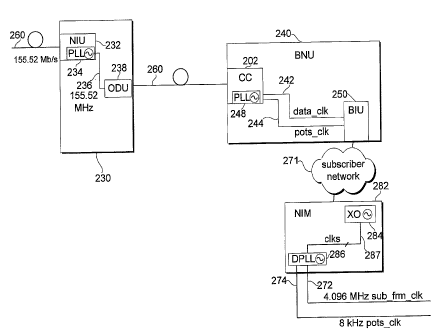
An embodiment for synchronization in a FTTC system is
illustrated in Fig. 2. At the BDT 230, a 155.52 Mb/s signal
is received on optical fiber 260. The signal is received by
Network Interface Unit (NIU) 232 which contains a Phase
Locked Loop (PLL) 234. The PLL 234 recovers, in conjunction' _
- with other circuitry within NIU 232, a 155.52 MHz clock signal 236
The 155.52 MHZ clock signal 236 is transmitted to an Optical
Distribution Unit (ODU) 238 which~transmits data to, and
receives data from BNU 240 via an optical fiber 260.
7,
J
CA 02245567 2001-04-12
Within the BNU 240 a Common Control (CC) card 202
receives the optical signal, and a PLL 248 on the Common
Control card 202 recovers the 155.52 MHz clock signal. Iri:a
preferred embodiment, a 19.94 MHz clock signal 242 and a 8
kHz POTS clock signal 249 are derived and transmitted to a
Broadband Interface Unit 250.
The BIU 250 transmits and receives data over coaxial
cable 270 which is connected to Network Interface Module
(NIM) 282. NIM 282 is part of one of the in-home devices
including the PID 294, television set-top 298, and computer
with NIC card 292. The NIM is connected to the BIU 250 via
the subscriber network 271. In a preferred embodiment the
subscriber network 271 includes the coaxial cable 270,
splitter 280 and in-home coaxial cable 272. In an alternate
embodiment the NIM 282 is directly connected to coaxial
cable 270. In yet another embodiment, the subscriber network
271 is a twisted pair drop cable connected to one or more
devices in the residence 290. The NIM 282 receives
downstream signals, an,d has a local crystal oscillator 284
which generates clock signals 287. A Digital Phase Locked Loop
(DPLL) 286 is used, 'in conjunction with the received data,
to generate a 4.096 MHz subscriber frame clock signal 272
and a NIM 8 kHz POTs clock signal 279.
In the upstream direction the NIM transmits data at a
rate of 19.44 Mb/s to BIU 250 on a carrier frequency of
38.88 MHz. In a preferred embodiment this carrier frequency
and the data clock are not phase locked to any downstream
signal.
FIG. 3a illustrates the clocks which are generated at
the BNU 290 which include a synchronous 155.52 MHz clock, a
downstream data clock 304 and a synchronous 19.44 MHz clock
308. As used herein, "synchronous" refers to a clock which
is.derived from a master clock, and is phase locked,
tracking the phase and frequency of the master clock.
"Deriving a clock signal", as used herein, refers to phase
8.
CA 02245567 1998-08-OS
t . . P 7 10 PCT ' ~ ~~. 10 APR 199
locking a lock clock to an incoming clock. Methods for phase
locking are well known to those skilled in the art.
FIG. 3b illustrates the clocks which are generated at
the NIM 282 and include a 19.44 MHz clock 320, a 38.88 MHz
clock 330, a 51.84 MHz clock 312 and a 77.76 MHz clock 314,
and a 155.52 MHz clock 300. In a preferred embodiment 25.92
MHz, 9.72 MHz, and 6.48 MHz clocks, as well as a 7.776 MHz
processor clocks are also generated. When used herein, the
term "generated" refers to a clock signal which is not
necessarily phase locked to another clock signal.
Transmission of data from BIU 250 to NIM 282 takes
place by modulating downstream data onto an RF carrier.
Both the carrier and downstream data clock are integer
multiples of a sub-harmonic of a master clock at BIU 25 0.
---.,
In a preferred embodiment, the master clock at BIU 250 is
synchronous 19.44 MHz clock 308, the downstream data cl ock
is 51.84 MHz clock 304, and the downstream carrier is
a
19.44 MHz signal generated from 19.44 MHz clock 308.
Other clocks which are integer multiples of sub-
harmonics of the master clock are generated in BIU 250 and
used for analog to digital (A/D) and digital to analog (D/A)
conversions. In a preferred embodiment, A/D conversion of
the signal received at BIU 250 takes place at 51.84
Megasamples per second (Msps)and digital to analog
conversion for transmission of data takes places at 77. 76
Msps.
Data is received over the subscriber network 271 at NIM
282, and is digitally sampled. In a preferred embodiment,
the sampling of the received downstream data takes place at
a rate of 77.76 Msps. Digital fs/4 downconversion is used
subsequently to produce baseband signals. In an alternate
embodiment, an analog downconversion is used based on a
38.88 MHz signal for generation of I and Q baseband signals,
and the baseband signals are sampled at 25.92 Msps. Further
digital processing is performed on the received data using
multiples of a sub-harmonic of 19.44 MHz clock 320.
9.
~~~~~fo sH~~
CA 02245567 1998-08-04
WO 97/28611 PCT/US97/01996
In a preferred embodiment, transmission of data from
NIM 282 to BIU 240 takes place on a carrier frequency of
38.88 MHz, at a data rate of 19.44 MHz. Integer sub-
harmonics of 19.44 MHz clock 320 are used to generate both
the carrier frequency and data clock for upstream data
transmission. Analog or digital techniques can be used to
generate these clocks. '
In a preferred embodiment processing of data for
upstream transmission from NIM 282 takes place using digital
to analog conversion a rate of 155.52 MHz, using f8/4
upconversion to arrive at a carrier frequency of 38.88 MHz.
In an alternate embodiment, I and Q baseband signals are
constructed using D/A converters operating at a 19.44 Msps
conversion rate using 19.44 MHz clock 320. The baseband
signals are upconverted using 77.76 MHz clock 314.
The clocks at BIU 250 and the NIM 282 are not
restricted to the aforementioned clocks. Other clocks can be
used for internal operations such as D/A and A/D
conversions, as well as for establishing the data rate or
carrier frequencies. In a preferred embodiment, 19.44 MHz
clock 320 is not phase locked to 19.44 MHz master clock 308.
In an alternate embodiment, the 19.44 MHz clock 320 at NIM
282 is phase locked to 19.44 MHz clock 320 using phase
locking techniques known to those skilled in the art. The
advantage of phase-locking 19.44 MHz clock 320 at the NIM
282 is that it reduces the frequency uncertainty of bursts
of data arriving at BIU 250, and enables longer bursts to be
recovered successfully.
A method for the downconversion of upstream burst data
received at BIU 250 is illustrated in FIG. 4. Referring to
FIG. 4, the bandpass input signal A20 is sampled at 4/3 f~up
in step A20, where f~"p is the upstream carrier frequency.
This technique is referred to herein as f5/4 downconversion,
since after such sampling the inverted spectrum is now at
f$/4. This technique can be used as long as the band below
f$/2 remains clear before sampling .The real sampled signal
10.
CA 02245567 1998-08-04
WO 97/28611 PCT/US97/01996
is multiplied by e-~n~"~2~ A30 which generates complex baseband
samples. This signal is interpolated in step A40 to
generate 3 output samples for every input sample. In an
interpolation step A40 two zeros are added between the data
samples. Interpolation when use herein means the addition of
zeros for subsequent filtering.
Step A40 results in I and Q data streams, each at
155.52 (Msps), which are low pass filtered A50. In a
preferred embodiment this is a root-raised cosine low pass
filter with an excess bandwidth of 35$ (a. = 0.351. The
signal is decimated by eight A60 to produce downconverted
samples A70 at a rate of 19.44 Msps.
FIG. 5 illustrates the I channel before interpolation,
Io 510; the Q channel before interpolation, Qo 515; the I
channel after interpolation, IINT 520; and the Q channel
after interpolation, QINT 525. In FIG. 5 the samples
generated by the AlD conversion are represented by xn. Each
input sample in Io 510 and Qo 515 results in three output
samples in IINT 520 and QruT 525 respectively.
The filtering which takes place in step A50 of FIG. 4
can be accomplished with a digital filter which has a series
of taps, also referred to as coefficients, which are used a
multiplier on the input samples. The output of the filter
is the sum of a the interpolated samples multiplied by their
respective coefficients. In a preferred embodiment, 132
taps are used to form this filter, indicating that 132
interpolated samples are used to calculate an individual
value for the output of the filter.
FIG. 6 illustrates the use of a polyphase interpolation
filter in the I channel on data II~,T 520. A polyphase filter
can be formed by grouping the taps to form a number of sub-
filters within the digital filter. Use of a polyphase filter
Fo requires Fo taps ho, hs, h12, h18..., continuing on to 132 or
the nearest integer below 132. Similarly, F2 taps are formed
from h2, h8, h19, h2o..., and F4 taps are h4, hlo, hls, h2a.... The
11.
CA 02245567 2001-04-12
output pf each polyphase filter, yn, is given by the weighted
sum of the taps of that filter multiplied by the respective
samples xn. The output values of the filters at instances yn
can be seen to be yo =xoho-x2h6+..., yl=-x2hZ+x9hs+..., y2=x4hq-
x2hlo..., Ys=xsho-xshs....
As shown in FIG 6, the advantage, of a polyphase filter
is that in forming the groups of taps, all taps which
multiply zero valued data samples can be ignored, resulting
in a simplified filter. All multiplies which have zero
valued samples xn can be ignored in the digital realization
of the filter. The final output stream of the polyphase
interpolation filter in the I channel is the interpolated
data at a rate of 19.44 Msps. The Q channel filtering is
also performed in this manner, and the resultant
downconverted samples A70 are the complex data (I and Q) at
a rate of 19.44 Msps:
Polyphase filtering techniques are well understood by
those skilled in the art, and are discussed in the text by
R.E. Crochiere, and L.R. Rabiner; "Multirate Digital Signal
Processing," (Prentice Hall, New Jersey, 1983),
Many of the steps shown in FIG. 4, when realized in
digital logic, will be operations on samples which do not
contain information (zeros) or can be realized by a simple
sign change or multiplexing operation. As examples, the
multiply step A30 in FIG. 4 is realized with multiplexor,
and many portions of the polyphase filter 600 shown in FIG.
6 can be eliminated. Similarly, when the decimation step
A60 is included in the synthesis of digital logic to perform
steps A20,.A40, A50 and A60, a significant number of
mathematical operations can be eliminated. Methods for
synthesis of digital logic to perform the steps shown in
FIG. 4 are known by those skilled in the art.
In one embodiment sampling step A20 of FIG 4 takes
place in a discrete A/D integrated circuit, and the
subsequent steps shown in FTG. 4 are performed in an
12.
CA 02245567 1998-08-04
WO 97!28611 PCT/U897/OI996
Application Specific Integrated Circuit (ASIC) in BIU 250.
In a preferred embodiment, the analog to digital conversion
takes place in the ASIC.
Although the present invention has been described in
' 5 considerable detail with reference to certain preferred
versions thereof, other versions are possible. The goal of
the invention as a method and apparatus for the
synchronization and downconversion remains the same however.
Therefore, the spirit and scope of the appended claims
should not be limited to the description of the preferred
versions contained herein.
13.