Note: Descriptions are shown in the official language in which they were submitted.
CA 02245862 1998-08-07
W 097/29507 1 PCT~US971~2042
MULTll~r IA DE~CIY)RS FOR MEDICAL IIMAGING
TI~I~AL EIELD
.
The present ~nvention is ~ e~ted to x-ray digital radiography, including dual-
energy imaging, computed tomography (Cr~ olomography and x-ray
mi .sc ,~, nuclear medicine, inclu~ing quanl;l,lLi~ autoradiography, single
photon emission tomography (SPECI') and positron ~mjr cn tol..o~phy (PEI~;
and bio-optical imaging, including optical confocal microscopy and optical
10 tomography. The i..~ n is more particularly directed to novel gas detector
media c~ on gas-mic~ principles for use in these ap~lic~t:~ns.
R~C~ROUND OF THE INVENTION
The capture and ~7etect;~n of ionizing rsdi~t:on in an ~m~ way, without
significant loss or de~ rl~tiQn of the hnage information, is of paramount
significance in m~ c~l imaging.
Recent advances in medical ~c tector terhr ~logy make it posQ;~ for superior
images to be pro~ll r e d by means of digital electronic techniques co p~red with
2û rln~ film-screen techniques. In fact, corQ;d~rable efforts are in progress to
develop new - -~s of .~II;G~hic ~ q~ing that utilize recent advances in
ele~lr~ ics and computer technology to ill~y~ diagnostic qualib and to evolve
new dis~grosti~ mo(l~liti?s v,~ith l~d~ced p&ti..ll dose. These methods are generally
known as digital radiography.
2~ Spe~ iff~ lly, digital radiography has many a~ g; S over the conventional
;o~ ,hy such as eYpDn~l~A display of detector dynamic range, fast image
~cquisition and display, COI~ t storage, tr~- ! ir 'C . and display of stored
images without degradation, extended ~r~hilities of data analysis and image
1~~'~ ; and reduced patient dose.
Dil~.~.lt detector technologies and beam ~ ries have been proposed for
digital radiography, cl~ssified such as s~intill~tor-photodiode~ high-pressure gas
filIed ~letectors, sl~int~ tor-photo~nllltirli~r~ kinestatic charge detector, ~o~-mity
image i~ CCD, phosphor s..~ - photodiode and diode array.
SU~STITUTE SHEET (RUI E 26)
CA 02245862 l99X-08-07
WO 97/2gS07 2 PCT/US97/02042
Some of the disaclvantages p es_ ~Iy ~aced in the fîeld relate to the relatiLvely
high initial cost of the digital ~ ~&phic systems, as well as to the l~mited
dete~tor ~ on. The ~et~tor system sho~ld be condit; -~ by des}gn c~
aimed at increasing sr~t~ u~al resolution and contrast r~sol~lt;c- detective
uantum efffciency (DQE) and the signal-to-noise ratio, while m~ir ts-iring
~Yf~ ~e t sampling rates. A careful desi~n and development of the detector wouldbe ~q~~ ~d to provide a beneficial ir~r~et on x-ray capture and their f-m
conversion into charge carriers.
SUMlU~rY OF THE INVI~NIION
In the ~ es ~ invention gas micJI~s~ detectors provide high spatial,
sl and energy resolution, ~ ltin,g from fine co"~ctQr size, double layer~~ geometly, and high gain. A spatial resolution less than 2~ may be
._d, wi~h count rates higher than 107 particles/mm2.
One object of the illvention is to provide a high spatial resoluffon, high
contrast resolution, dual cne.~, gas microstrip detector for digital radiographywhich - ~ases image qualib irl digital x-ray radiography ~ ~ling dual energy
20 imaging and pro~ides ;,..~ det~ti- of low contrast ~Ir~c~ s at equal or
Iower dose than film r..d:c~.~phy.
Another ob~ect of the in~ention ~s to provide a high spatial r~oll t;~n, high
contrast rcsq~ n, gas microstrip ~el~ lor for &ulc~ ~arhy which provides
higher sensitivity and lower exposure tilmes than film fi~ A~l;ography, and which
2~ also provides imaging access at the cellnl~r level.
Acco~ .g to the ~-~s.~ ve-llion, the apr~ hility of gas-dctect~
principles on both dual-energy ~L't~ ''~n~ SUClll as for chest radiography and
mammography, and q~ autoradiography may be employed in several
de~ or e~ho~ ~nts. Overall, tlhe gas-microstrip .'etect;on principles enhance
30 dramat~cally the image quality Or the digital dual f &~ deh~lor which may be
ap~lied to general-purpose digital radiography, computer ~cci~te~l tomography
(~), microtomography and x-ray microscopy, includingx-ray confocal microscopy.
SI~tBsTlTuTF SHEET (RULE 2&)
CA 02245862 1998-08-07
W 097/29507 3 PCTr~S97/02042
Also, the same gas--~el ~c~;an principles offer notable adv~rtagPs over film
~o ~graphy by providing a higher se..s~ , much lower c.~o~ e times, as
~vell as imaging access at the cellular leveL Therefore, enhanced radioisotope
~ imaging of either tissue sD~p'es, to detennine radiopharmaceutical distribution
S at c~ lqr levels, or of electropl ~ei,is plates, for determining molecular weights,
is enabled. In ~it-n~ the ~ seA~ . ti-n is applir-r)le to other areas of
r medicine, such as PET and SPECr.
In positron-emission tomography (PET) one has to efficiently detect 511 keV
annihilation gamma rays with optir~Ql space and time resoll-ti-ns. Tr~ n~ny~
~ages obtained with PET show low contrast. Moreover, PET does not provide
q7~qte CQ '-ng s~qti~t -~ in an -~c ~t. hle PYrosl~re time of a~ Y~ tf~ly 30
tt~s.
The most traditional a~ to PET is to use a photoml~ltirli-r coupled
to each NaI or BGO s~ qtion crystal. The sc;nt;ll~tj~n light (emitted in the
l~i nsible range) is ~1~ t~t~l by a pluralib of ~-t~ml~ltirl!-r tubes in order to cover
a wide solid angle with a good resolution. This increases the complexity of the
d~t~ t~r system and P~so~i-qte~l clc~llol.ics. It is obvious that high costs -q~soci~te~
with large numbers of photo~ liers incr_ase the cost of P~:T ml-lti' e ~ ~ systems
and fi~r;fi- q~tly make their use pro' ~h;te~
In image .1~ l e cti-tg systems there is also a need for a lu. cost efficient and
large sized imaging detector readout. It is known to provide ~le~tors based uponindirect conversion of x-rays or ~ .--q rays using sc~ tor crystals with
~' ~to-liodes or photom~lltipliPrs. However, this technology is either expensive or
results in m~ r~ e images. It is known to use charge couple device (CCD)
2~ . &S, but these have a small active area that limits s;g~ifie~ ly the area of
inle~ ';o-- F~lh~,.nore, a CCD camera offers a low qn~rt--m sink a low
signal-to-noise ratio e~ c:ally for low co..h.~sl applications.
It has also been known in other technologies to use several semi-co- d~lctor
media such CdZnTe semi-con-luclu-;" amorphous selPnil~ CdSe, or amorphous
30 ~ili~c However, these materials create other problems. For instance, a CdZnTed~ lu, which has a high atomic r r~hPr and density that results in a high
~un--t~m efficiency, ~ ro~ tPly provides a poor collection '-Pf~;A~y~ As a result,
even if the detector is char~ l ri7ed by optimal detector quality parameters, noSl.la$TITUTE SHEET (Rl~LE ~i)
CA 02245862 1998-08-07
W 097/29507 4 PCTrUS97/~2042
optimized ce-~- or impurities ~n the ~ale.ial result in an i~ r performance.
It is highly desirable that a d~tector exhibit linear current-voltage charact~ t~- 5,
This can be achieved only if the semi-conductor medium has high resistivity and
the ~ t~ tC are ohmic- In contrast, r- okmic contacts (~ clringco t~ t~) lead
to the formation of ~ -t~ky diode det~ i s. These d~ lo s e~hibit no~ r
2 r charactt ~L;slics which are highly, r ~Q;rable. Also, inJecting c n ' U ' ~, act
as an oh c contact at low applied electric fields, but at a high applied ~Icch;cffelds the ~l~tectell current is space-charge limited which is an undesirable effect.
Generally, several contact studies based on electroless gold and e.a~a aled
10 metallic r~ t' (gold, indium, zinc and ~ contacts) with the CdZnTe
surface ~as;,i~ated or passivated have been sh-d:~ d However, no optimal contactfO l~t; has yet been found.
It is also well known that the high cost of a c~ystal scirf ~ tor
photomnltirl /microchannel plate system makes their use prohibitive in medlical
l!; imaging appli-- - where a large ~l-Pr of ~eterte~ ~ are ie~ d.
Spee;fi; lly~ these deviees ean ol3Eer ..~.ag~ to-high quantum efF ~ and/or
srlrl~;c~f~on~ but also with a high or even prohibitive eost by virtue of the large
l~r of ~L~t~dclec~-ve ~ s r~uir~:d. ~A(l;~io~ ly~ in some appli~tions
photomultipliers are prone to unwanted stabilities due to high applied voltages or
20 too strong m-O ~ti~ fields. Sueh deviees are used for -Ic-r me~l; ' ?,~ ray
astronomy and seientifie appli.~S-t;- ~.
The detection prineiples of the ~ . t;on may also be employed for
the direet convel~sion of x-rays or ga~a rays to an rl~f ~ ;C eharge. By coupling
the gas microstrip with a semieonduetor substrate an efficient ch&~o_ ca~LIier
2S ~ete-~ti-n and coll~t~ system of virtually any size ean be provided. This
approaeh provides higher image resolution at a lower cost than e..~ g
systems.
In P -tl~r use of the ~ 3C~.-I ~nvention's d~tecticn principles a gas
~S~rlp substrate eoated with a pv ~ le ,-,&te.;al may be eoupled ~
30 to a scir~ ti~ e~ystal or scir~f~ ;ng fiber, or indir~ via a fiber optics
systern. This eonf1O~ ' ~In provides a low-cost alternative to conVPnt;onS~l
~ o-n lt;r~;~rs ~nth ~nh~nce~ stability and ' ~n~ cnr~hilit;~ his
col~G~ .tion also provides an alternative to charge coupled devices (CCD) by
SU~TlTUTE SHEET (FiULE 261
CA 02245862 1998-08-07
W 0 97/29507 5 PCTrUS97/02042
providing a high quantum sink, a large dimensional array and high gain, re.~ s
that cannot be provided by a CCD camera.
In one embodiment of the invention, dual energy radiographic detection is
performed with a single x-ray ~c, ~ which produces high and low energy images
5 ~;~nltsneously. By ~ lt~ eGusly providing high spatial resolution and high
contrast resolution, an i~ vved sensitivity, spe~ifi~;ty of ~ t t-n, and
character zation of the tissue abnormality is obtained. ~ ~lditi-n~lly~ a dual energy
~tecto may be o~_...ted under open beam or scanning beam geometry.
The foregoing and other ob3ects of the invention which shall become
10 apparent as the ~I t~ilc(l description ~ occcds are achieved by a gas microstrip
detect~r which .~c~ s incident r~ t~ through a ;,.,I~;c~l to generate an image,
comprising: a substrate having on a first ~u.~--e a plurality of alternat;ng first
anode means and first cathode ~e~n~; a ~letector c~ ~le spaced apart from and
~osi,~5 the substrate first surface; and a zone for ~licposing a gaseous - -
1~; between the SU~DII ~te and the ~ r cathode and for r~,C~ ~ incident radiation
~ p= 1~ through the ~ ~e:~l
The l l~sc.ll invention also provides a method for obt~ir ing an image of asubject ~osed to incident radiation comprising the steps of: exposing a ~ lector
to ~ r~ projected through a s~mrle~ wherein the detector comprises
20 a gas microstrip detector, including a substrate having on a first surface a
plurality of alternating anode means and cç~l e~le means, a detector r~t~o~e
spaced apart f~om and opposing the sub~lr~le first ~ -e, and a zone for
~i~pos ng a gaseous medium between the i...b~ le and the det~_t~ cathode and
for ~c~ vi~ t radiation from the sample, ~ hc~e:n the incident r lis~tion
25 produces photons by - - ~ of the gaseous medium; abso~ g the photons in
said detector to form an ims-ging signal; and producing a digital image from the lg signal.
Other objects of the invention are apparent from the ~ nil?~l description of
~ the invention which follows.
SUBSTITUTE SHEET ~RULE 26
CA 02245862 1998-08-07
W O 97/29507 6 PCT~US97/02042
BRIEF DESCRIPTION OF THE DRAW~IGS
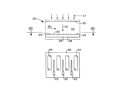
Fig. IA is a schematic side elc...lional view of a gas microstrip ~lel~lur.
Fig. lB is a top view of a gas microstrip ~ete~for. '~
Fig. lC is a schematic diagram of a gas microstrip imaging system.
Fig. lD is a schematic side elevational ~iew of a gas microstrip dr~ecfor
c~ ,r~ ~ with x-ray dir~li~ dences.
Fig. 2 is a quasi-dipole configuration of the e~ c field ~ gt' est~hlished
_~ an - ~d~ sP'~ e pair Or a ~ sl,~ cQ-f, '-
Fig. 3 is a ~ ecli~_ view of a dual-energy gas mi~ U~ 2Ct- .
Fig. 4 is a r-' -r~~ti~ ~ S~ n of a dual-energy digital radiographic
system based on se~ t~ gas microstli~p ~ete~t~ principles.
Fig. ~ is an exploded pe~ ,e~ v ew of a gas-microstrip delc~C~ ror
quanlilati~ autoradiography.
Fig. 6. is a ~p'~ fion of the energy absorption efficiency with
increaslng xenon ~ es;,..re (d = 1 cm, E = 18.6 keV) suitable for mammography
a~td quanlil&li~ hy appli~ ts
Fig. 7 is a gr~p~ t'~n of the energy absorption ~ffi 'e ~ with
i~icreasin~ ~ .s~ ~ (d = S cm, 13: = 18.6 keV).
Fig. 8 is a gr~rhi~ .es~ n of the energy absorption ~ff;C;cncy with
increasing xenon ~ s~ (d = S cm, E = 50 keV~ fluence = 2200 photons/mm2
F~.itDhle for chest, - ~lic~ hy.
Fig. 9 is a gr~ '- of the signal pro~lr-~ed with ~ ,&Sil~g
2c~non pressure (d = 1 cm, E = 18.6 keV, fluence = 2200 p~-t~ -s/mm2) e"~;tS~
25 for ~ e &~.lol~ ~iography.
Fig. 10 is a graphical r~ s~ ~ti~n of the signal produced with increasing
xenon ~ es~ur~ (d = 5 cm, 13: = ~0 keV fluence = 1.08 x 10⁵ photons/mm2)
suitable for chest radiography.
Fig. 11 is a grap~ s~ t;~n of the gain in argon with increasing
30 ,1~l 'ie ~ voltage, at di~ferent D r~ r ~ e ~ r~es, at 1 atmosphere.
Fig. 12 is a grap~ c~ n of the gain in xenon with increasing
applied voltage, at ~ ' anode c=~l~oAe ~ es~ at 1 atmosphere.
~l~3TlTUTF S~lEEr (~U' E 26~
CA 02245862 1998-08-07
W O 97/29507 7 PCTrUS97/02042
Fig. 13 is a gr~p~ l r~ ;or~ of the gain with in~,~as~.g ~,es~e, at
different urpl - ~ vQ~t~gPs> with an anode radius of one micron, and an anode--
cathode distance of 10 microns.
Fig. 14 is a graphical representation of the electric ffeld on the surface of the
S anode w th increasing anode radius, at different Q-~e cathode distances, at ani~d voltage of 400 V.
Fig. 15 is a s~h~t;~ representation of a microstrip ~l~tectQr used in
positron ~ic~;on tomography.
Fig. 16 is a ~ ,e~ view of a hybrid solid state-gaseous microstrip.
Fig. 17 is a schematic ~ s~ntation of a gas m ~ .strir c_ '~3 to a
scintillation crystal for use as a p'r~t~ ~~plffier ~ to the present invention.
Fig. 17A is a ffrst alternative p'~otQ~mr~ r acr .lil.g to the present
invention.
Fig. 17B is a second plterr~tive photoampliffer according to the ~ ~s_..t
15 invention.
Fig. 18 is a schematic ~ 3~ of a gas micf~-~r~p coupled to
scintillating ffbers for use as a photoamplifl f r~ding to the ~ ~s_..l invention.
r~~-- EMBODIM~NTS OF l~IE INVI~TION
The il-~ tiVt: imaging device comprises the front end of an imaging system,
namely the gas mie..J~rir detector. Gas-microstrip ~l~te~tQrs provide ulL~
resolution, high internal gain and low noise, and high rate devices, for co-rting
and imaging applications.
2~; Fe l ~s of the gas microstrip device include:
i. Providing an ~Ir~ high spatial r~col~lt~ due to the micron or
sv~ n size of the ;. -~..g signal colle~tors.
ii. Providing an c~ !y high position resolution in the x-y plane, if
required, due to the back side sensing electrodes.
iii. Providing a high contrast r~eolllt~on due to the ~prl;ed dual energy
detection principles.
SUBSTITUTE SHEEr (P~ULE 2~3
CA 02245862 1998-08-07
W 097/29507 8 PCT~US97/02042
iv. Providing high sensitivity, that implies a high detective ~lln -
efffcien~y (DQE), due to the very high and noiseless internal ~rlrlifi~ff~n of the
signal in the gas medium.
v. P~ z elim - - of electrostatic in~n~; ?s~ due to the applied
S phcto- - ~graphlc techniques, which ~tilize microstrips i-~t~~~ of wires.
vi. n~ ~ ~ed cost as compPred to other microstrip s~ - h to;
t~
vii. The ability to be built in very large sensitive areas.
The inventive Dnag~ng device ~1i9 Icsed herein may be used in conj~r~t~
with ~ d~t- ~ ., t~ ~r~ , q~ '-' ffve autoradiography, x-ray and
light lmicroscopy, ~o~ tc -~ pl ~, solid state devices and
photoamplifiers ~p~ ,~d in medical imaging, bio-optics, ~ os~nrç, ir ~ ~nl and
other related applic~ ns.
Gfls Microstrip D~ t~lu. s
The fabrication of microstrip detectors ~~ffli7~s photolithographic te~hniques
commonly used to f~l ;cale -- ~' ' s ~or the s~m~ u ~tor 1n~ .y. V-leWS of'
a gas microstrip ~'et~tor 20 are shown in ~igs. lA and lB, and a schematic
20 diagram OI a gas ...i.lo~ lor imaging system for r~o~ I imaging is shown
in Fig. 1C. The Fig. lA collr~ dtion is l~f~ d to as a scanning beam ~"~ t~y
although an open face geometry is possible. The detector 20 repl~~es anode-
e wires with ultrafine depositi~ns of COl ~ ;ve strips, arranged in an
anode-cathode pattern on an i~ tin~ or partially l~ting glass substrate.
In the l~r~ 1 invention, a plurality of microstrip anodes 22 are i~le,l~e~ved
with a plurality of microstrip C11t- ~des 24. The anodes 22 and c~th~ s 24 are
photoli~ho~ ~pl~ ny applied to an insulating or partially in~ t;ng substrate 26.The ~..L~ Ie 26 may be a c D~ tive glass or plastic or an electrically cor~
layer on the surface of a semi~ u~ tor. In one embodiment, the microstrip mask~0 ro ~es cQ~ anode strips, which has a width in the micron range and
d ~th ~nder CQ~ C~ e strips which are also in the micron
range. Both anodles and cathûdes may be coated with chromium, gold, other
metals or the like. Depending upon the imaging applic~t cln, the width of the
SU3~;TITUTE SHEEr (RULE 2~i~
CA 02245862 1998-08-07
W O 97/29507 9 PCT~US97/02042
anodes and cathodes may be varied acco,di~ . An clc~lr c pote~ ff~l (not shown)
t~ s ~~ .. the anodes 22 and cathodes 24. On the side of the substrate
26 opposite the anode and cathode strips 22, 24 and oriented su~stS~ntis~lly
licular thereto, a plurality of back electrode strips 28 may be provided
5 depending upon the particular end use app'icr -n of the d h ~t~r. n ,~ n"
upon the end use, the back ele l,ode mh~uslr;lJs 28 may be used to provide
position resolution and imaging capql lit;~s in the xy plane. The width of the
back electrode strips 28 may be varied ~epe~ ing upon the imaging app!ic~tion.
Those sl~illed in the art will a~.~;ate that the substrate 26 is thin enough to
10 allow induced signals on the back electrode strips 28. ~r ~e~l signals may also
be ~ d by rili7in~ a substrate with a~,o~..file resistivity. As mentioned
previously, the b. l,~I.ale 26 may be a conductive glass or plastic s~sl-ate with
suitable de~lr - -' conduction ~ lies or the substrate may be provided with an
elc_l~ -lly conductive layer on the surface of an insulator by means of ion
15 i~npl~nt~ti~ or ~lepos;t:~ln of a thin film of semilonfll~ctQr material. A detector
r~tl~ode 30 is opposed to the substrate 26 ~h~ an electric field 32 may be
applied between the d~tector ( ~f~ e 30 and the plurality of back cle~lrode strips
28.
A gas - ~ 34 is; ~ te~ . the ~etector c"t~o~l~ 30 and the
20 substrate 26 in a manner well known in the art. The ~i~t~n~e 1~l-. ~ the
substrate 26 and the ~lPtector c~t} Q~l~ 30 is typically in the illi..-PtPr range,
although other SF--ing may be employed. The gaseous medium 34 may include
argon, xenon, krypton and mixtures thereof, as well as such inert gases or theirxtures in com' - ~t;~n with polar or ~1 ~ ng compounds in a dopamt
25 c~ r - dtion. The gaseo ~ - ~tl 34 may-be; - l~te(l at high ~ S~ e, if
required by the ;. ~ g appli~~tion to provide a high ~rn- efficiency and a
limited electron range.
A plurality of primary electrons, r~ese te~l by an arrow 36, are produced
- by direct x-ray ionization of the gas ~edimn 34 and are driflted toward the anodes
30 22. When the electrons 36 reach the electric field 32 ~a~ .. the re~liv~: anodes
22 and ~ a" ~ ~es 24, the electrons 36 drift toward the a~lu~riate cathode 24 where
they experience an avs~ amrlifi-~ti~n at F~ ntly high field strength, due
to the quasi-dipole anode-cathode configuration.
SU~;TlTUTE SHEET (RU~
CA 02245862 1998-08-07
W O 97/29507 lo PCT~US97/02042
As will become apparemt, the high degree of ~ hiwed v,~ith the
pl -t~ ~aphic te~ ~ ensures that the ~d~t e tlur 20 has ~AIl~ ~eJy high gain
over large areas which heretofore had been unavailable. VVith this technique it is
possible to make very p ~.ise thin strip &I~ res (anodes and cathodes) in the
lcron (1/1000 millimeters) or submicron-range, up to 1-2 microns, w~th a
t~- of 02 microns, which adhere ve~ well to the glass substrate. In
addition, it provides a high contrast reso~ t~ dlue to the 8p~ 7 dual energy
~ti~n principl~es.
As seen in Fig. lA, a plurality of x-rays 37 may be applied in planes parallel
to the ~d~ r in a strip beam geometry. Altematively, the x-rays 37 may be
~prli=~ normally through the C~ltl ~'- 30 in an open beam g.~
The ~etecto~ 20 may also be provided with a ~s-p;ll-~ry optic system 38 or a
Kumakhov lens 39 disposed between a source of the x-rays 37 and substrate
26/---~ e-le 30 as seen in Fig. lD. These directional x-ray devices may l~e provided
in either a stfip beam geometry or an open beam geometry. The r~, ~ll~ry optic
systeln 38 ~ a plurality of light fibers that collimates the incident light or
radiation. The low angQlar ~ .C~ e of capill~ry x-ray optics, due to the small
critical angle l~or ren-c~iQn~ provides the IJ~t~ 1 for extremely f~ t scatter
~e",!~ ''C'- with lel&~ high ~ ;~&~ tr~ A K1~nDkhOV lens 39 also
~unctions to collect and guide x-rays and the like into the gas ~edil-n7 34. Use of
these gui~ e me~ ri~ms further enhances the clari~y of the i- ~;..g signal.
a gas microstrip i~ system 40 of the ~, er~ vel~ivl~ shown in Fig. lC, an
x-ray tube 42 generates a pluralib of x-rays 44 which impinge on a person or
subject 45, that is, a biological or phal -~e~ --I sample, or a p~ti~, and pass
25 to the gas ~; os~ t~tor 20. An imaging signal produced by the detector 20
is passed to a ~ 46, Ih~.J g! a filter 48 and then to an ~mrlifi~r 49. The
imaging signal is directed to an oscilloscope 50 for real-time display and/or a
computer worlr~tirn 52 for data arl ~;t;on, analysis and storage.
Fig. 2 shows a quasi-dipole co~r,~ lion 58 of the electric field ~Ir~..gl1
30 est~ h~(l between an ano~e~ o~e pair of a gas-miclo~ co~ ration,
wherein ckc~.ic field lines are ~esigro~e~l by numeral 56 and potential lines are
des~ ted by numeral 58.
Sl~;TlTUTE SHEET ~F~ULE 2~)
CA 02245862 1998-08-07
W O 97/29507 ~1 PCT~US97/02042
nual-Ener~v D&tc;lion Techniques
Dual energy radiographic ~f~h~iques have been applied to imaging for
mammography and chest radiography. The dual-energy r~Ai~aphy removes the
'age contrast between any two chosen materials. By simplifying the background
5 structure in this way, an increase in the ~l~te~t~~ lity or "conspi ty" of the target
is oht~
A major limitation in conventional chest in aging te -- iques is the presence
of unwanted interfering structures. Sp~;fi~ " o.~,l&~ g projections of other
body structures such as Fibs, can obscure or camouflage the pulmonary nodules.
10 Therefore, tumors may not be clearly differentiated from adjacent ~ .1UI~S.
Dual energy digital radiography permits c~~ ell~firn of the displayed
contrast of any two m~t~ri~lc, such as bone and soft tissue, allowing low-contrast
lesions such as such as solitary pulmona~y nodule (SPN's) or 3 ~ ~ed ~ s~y
nodules (DPN's) to be obt~ through in~l~ased cQ-~cp;r~-ity in bone-canceled
15 images. Also, c~ lesions may be .lifrt~ tetl, therefore, lul~-ols may be
clearly dirr~ t~e d from adjacent structures.
This is useful since the ~,ese,.cc of c~l~ifi--ti~ in an SPN is the most
important determinant of l~enigr~ncy. In ~ldit;on~ fine, diff~sed c~lrific~t;ons are
often only ~ te -l ~e via-dual energy te~ ?r Dual energy may Ihc . ~ be
20 viewed as a techrique to maximize the diagnostic information ci I of the x-ray
image.
A major limitation in conventional mographic te~h-~iques is the
cs_..ce of unwanted il-te~re.i,-g structures. Spe~ifi~ y~ in mammograms
obtained with the compression met~ocl, normal soft tissues of breast, tumor,
25 calcium d~osils (e~ fi~tions)~ and other ~ may overlap one another in
such a way as to mask a lesion. Therefore, tumors may not be clearly
ted f~ j5 ~~-~t mammary ~ t es. VVith the use of - ~~raphy
in dense breasts, it may be ~liff;cl~lt to reco~i7P the border of cancer infiltration.
- Breast c~lc~ tiQns ~etected in many women undergoing m ~rnlnography can
30 be either benign or ~Q~ nt, which in~ -tes the presence of breast cancer. The~ect n of m~ nt c~lcific~tions is often the only way of making an early
Ss;e of cancer. Cancers may be r i~sed~ however, when c~l~ific~tS~ns are
ol)s~ by a "~lull~ed" background, res-~ltin~ from the contrast between the soft
~ SU8~;TITIJ~ESHE~(~ULF~;)
CA 02245862 1998-08-07
WO 97129507 12 PCTrUS97/02042
tissues in the breast. Reca~qe of the si~;f; -~nre that the yl. ~e of ~n~ tir
has in the diagr~o~i~ and ~lini~l evall~ation of breast cancer, such new t~-' ri~iues
for enl g ~ ~g breast images are of primary importance.
In digital dual eIIergy mammography, the ~ ;on of cnlr;fi~n~i~ns may be
S enhanced by removing ~Ir~ - t al noise fromi the surrounding so~t tissue in the
breast. Acco ~g to the in ~on~ dual energy radio~ ~ te ~n is
perfonned w3th a single x-ray exposure, producing high energy and low energy
images ~ aneollsly, thus eliminating misregistration problems or raff~nt
motion problems that can be present in double x-ray ~a e. A ~ e-l
subtraction of these two images wil} produce a digital image which eli3minates
either rnl~ or soft tissue.
The pnnciples of dual energy detection operating on gas r~
principles are shown in Fig. 3. The contrast resolution Or the systemi is
demonstrated by means o~a mammographic phantom designed to &11~ rte x-rays
lS in the same way as a human breast comllrcssed to 4.~ cm. A gas mic.osl~
A te to 60 provides a plurali~ of back electrode strips 28 on one side of the
substrate 26 and the anodes and cathodes on the other side. Tllie pluralib of back
elccLIodc strips 28 are separated into a front nLicrostrip zone 62, which absorbs
a ~ate, ~ f ~ g~ of low energy x-ray photons 44, and a back microstrip zone
64 which Qh~lrbs a greater ~el~r~ ' 1~ of high energy x-ray photons 44. The two
m.~.~,sl.i~ zones 62 and 64 are separated by a neutral zone 66 (gro~ de~) to
increase s~ffit'ently the mean ener~y separation of the two jm~ging ~ignals
generated by their ~ eclive zones. The sublr~clion of these two signals results
in an enhanced detecff~- of microc~lrific P l ta:l!s by removing ~ red noise from
the surroundling soft tissue. A c plete small-field of v~ew (SFOV) jm aging system
is th~ ffo~ enabled, through this ~
A diagram of a dual ~ _.~, digital radiographic system based on segmented
gas mh~v~ ~tio~ r ~l~C is shown in Fig. 4 and is ~leciO0~te~l generally
by the numeral 70. A dual-energy gas-microstrip detector 70 o~e,~tes by
iS~jJ~ g the signal-coll~ti~ ffmgers inside the detector into the following three
zones: a f~ont zone 62, an inactive neutral zone 66 and a back zone 64. The ~ront
zone 62 produces the digital kJ. -~ - ~, hnage and the back seO le~t 64 producesthe digital hE~ cncrO~y image. The purpose of the inactive neutral zone 66 is to TUTESH~ET(F~U~ - 2~
CA 02245862 1998-08-07
W O 97/29S07 13 PCTrUS97/02042
harden the x-rays and Ihc.eL,. increase the energy separation 1~ the low and
high energy i~ag~s. A prefilter ~l~t~ ial 72 with an a~,~.~,. ;atel~ chosen k-edge
is placed adjacent to the x-ray tube 42 so as to produce a bimodal x-ray ~C.Ir r"
- entering the ob~ect or p' ~ntom 74. The dual-energy microstrip ~leteetor 70
5 cc rri~es an ~1 ~ x-raywindow 76which encloses the gas ~-rJ;r~.. 34. The
~etecte~ signals are ~lnplif~l, fîltered, and then displayed on a digital real-ti ne
osc~ sr~e.
On~ ~utoradio~raphy
10Several biological ~- C~rement and detection terhr iques in nuclear
medicine ~pen~l on the ~ntit~tive ev~ln~ lc.. of radiol~h~lled subst~n-~es in two-
nal separated media. Film based terhl iques are ~ pPn~ive and
il 'e but are li~nited to the study of only certain biologic~l compounds.
.ling to the invention, a new ~ te ~.c is ~ es -~ which offers notable
15 advantages over film autoradiographywith a higher sensitivity, i~ d ~etect;~ n
f~m ~, ~e ~ased exposure times, and imaging access at the cf~llr lnr level. In
fact, the inventive gas-microstrip device offers ~os~-res times over 1000 tisnes less
than film based methods, as well as higher gain and stability when comr~red to
aV~r~ -~ c photo~l~tectors and vnre proportional counters. Therefore, f~n~ -Fd
20 ra~ icotQpe ;~ g:-~g of either tissue ~nmp'cs to determine radiopl,&r. ~re-
~distril ~;-n at cellular levels, or of electro;21~ is plates for determining
mole lf-r ~ hls~ is provided.
An ~rrmrl~ly detector A~s.~ 1 for ql~nt;t~t;ve autor~A o~aphy is shown
in Fig. 5 and is ~le i,_ -ted general~y by the numeral 80. The detector 80 operates
25 in much the same ~ -~ as the other detectors p~~s~ ell hereinabove. In this
emho~iment a r~Ai~ plate source 82 is employed to emit weak radiation
which ionizes the gas ~ r~ 34 that is; -ap~ l~te(~ .. the plate source 82
and the substrate 26. A grid plate or d.t~clol cathode 83 is ~ posed bcl~._e.- the
plate source 82 and the substrate 26 in a p}ane suhs~ lly parallel thereto. In
30 the I ~ d ~mhoAiment~ the grid plate 83 is separated from the plate source 82by about .5 mm. Of course, other sp~cings may be employed. The electrons
Oer ated are drifted under the influence of an applied electric field generated by
SUBSTITUTE SHE~T (RU~E 2~)
CA 02245862 l998-08-07
W O 97/29507 14 PCTrUS97/02042
the detector cathode 30 and the pll~rality of anodes 22. Electron amp'iff~tir~ and
collection occurs in rl&tiveAL_u~ to the anodes 22.
D~te~LoA Examples
The energy absorption ~ffi~;~ s versus opeA~ ~ gas yr~oo~es are shown
in Figs. 6 - 8. In Figs. 6 and 7, the energy absorption efl~ - os for a ~ lled
.e~ecto~ have beeA~A estimated at 18.1 keV ~nammoA~Auhy and quanlilhli~t;
graphy)~ vfith an absorption depth Or 1 cm and ~ cm, A~e~Aue~ . In
Fig. 8, the energy abso~ption e~ficiency for 8 xenon-filled detector has been
estiAmated at 50 kev (chest radiography), with an absorption depth of 5 cm. It is
obs~ d that energy abs~ Aulion ewiri~n~1es up to 85% can be obP e~l for xenon
~as ~rtector media pressurized up to 10 atmospheA~es with a detector depth of S
cm. Of course, higher ALAeO !i~Ar~ s can be rtili7~-l
The signal produced with increasing gas ~. es~ is shown in Figs. 9 and 10.
In Fig. 9, the AL ~d -~t~ signal in a xenon gas-filled A~ OSt~ P detector for anabsorption depth of 1 CA~ a photon ll~ v, ~ c of 2200 photQr~/mm2, and a gas gain
of 10S at 18.1 kev is shown. The pro.~ -e 1 signal in a xenon gas-fflled microstrip
~lr~ertQr for an absorption depth of S cm, photon ~ e of 1.08 x 10⁵
photons/mm2, and a gain of 10S at 50 kev is shown in Fig. 10. Although a galn of10~ is ~ ~?' ~ gains of several magri~ldes higher are pos~ with the microstrip
e'~
In fact, the gas mnltirli~~fio~ factors (gain) with increasing applied voltage,
for argon- and xenon-fflled microstrip drte~tors, at 1 ~ -sph~re and different
anoc'e ~ o~le ~ " Ps are shown in Figs. 11 and 12"~sAue~ . The gas
~--lffrli--tio~ factor vvith increasing AuraOure~ at diA~eA~ applied voltages in~cenon gas fflled ~lPI~ofs, with an anode radius of one micmn and an anode-
cathode ~ict~n~e of 10 microns, is shown in Fig. 13.
The ck_l c field at the surAface of the anode with increasing anode radius,
at d;Arr . ano~.c ~ ' ~de ~lirt~r~es, at an applied voltage of 400 V, is shown in
Fig. 14. Overall, it has been observed that the quasi-dipole co~fig.-~ ~lion of the
anodc~ ' o~ Anic~,s~ gives rise to a hAgh electric-field slA~ ~h that
co~ l"'S to high signal gain with a relatively low applied voltage. Rer~n~e of
the small ~submicrometer3 strip size and the short ~ n~ time of the ions, the
~SU~STITUTE St lEET (RULE 26J
CA 02245862 1998-08-07
W O 97/29S07 15 PCT~US97/02042
gas-microstfip technology offers unique pulsed ?dic~ lg appli~t~ns for
nuclear medicine at high rates. Also, the ~ypose~l detection techniques have
unique image quality properties that enhance the current dual-energy -' I~ti~
techniques significantly and have an impact on the Imaging quality of an x-ray
!; digltal ~ ~iographic system.
-
Positron Fmi~sion Tomopraphy
A positron ~mi~ ~n to---o~phy (PET) imaging ~etec~or comprises a
s~inti~ or~ such as a BaF2 crystal, coupled to a IOW~ D- ~ inert-gas filled tube10 which ~e.~tes on excited state p' ~ i7~t;-n principles. The gas ~e~ectQr is
o~ led in the k-~ eQ~ ~o..n regime, which can be achieved by using a ~,I&Ii~
low bias voltage. This regime is m~int~ (l upon the appli= ~t;on of a relativelylow cle ;c field and gives fise to e~cited rather than ionized atoms which
characterize the gas response as excited state photoion 'i-n. The DC component
15 of the UV photons add to the ~ ;on produced by the bias and permits
operation of the ~ te- ~lr at slightly lower bias. Since the gas ~etertQr can operate
at an ~Il. --ly low bias current (nA), the prebreakdown regime may be very
sensitive to rh~rlg~s in incident power.
According to the present invention, a PET device, des;g.-~tell generally by the
20 numeral 100, is ~I~S~ le~l in Fig. 15. The device 100 inrllldes a photo-tube 102
which is filled with a gas 103 such as argon, xenon or the like and ~irt~in~l ata low I ~S~ul~. The device 100 i~ es a primary ~1etectjc- reg}on 104, a transfergap 106 and a l '~l e l 1 readout circuit 108.
The primary 1'~1 o ~ ~n region 104 provides a par~l-lripe~l~l BF2 crystal 110
25 which in this e~nho~liment is 25 X 45 mm2 and 8 mm thick. Of course, the crystal
110 may be any appropriately related material known for ~ne~lie~I imaging
applic~ . Disposed underneath the crystal 110 is a reverse bias zone 112
which CQ~ tS of a grid of wires 114 which in this embodiment are 50 ~m Mo
wires at 0.5 mm pitch. Tne grid 114 is positioned about 0.5 mm away from the
30 crystal 110 to ~ charge build up on the c~gstal surface. A voltage source
(not shown~ of about -30V is connected to the grid 114 for this purpose. The
region 104 r~hcr ir(~ S a conversion zone 116 which may be from 0.5 to 3 mm
wide. A pluralib of planar wires 118, which in this embo~liment are 50 ,um Mo
SU~S~ITUTE SHEE~ (RULE 26~
CA 0224S862 1998-08-07
W O 97/29507 16 PCTnUS97/02042
wires at Q5 mm pitch, are ~ osed und~ the ce ~ ,ion zone 116 and are
maintained at a voltage of about ~100 V. A preamrlifir-ti~ grid 119 is spaced
about 10 mm below the con~. ;.e~ zone 116. A metallic mesh of wires 120 is
pose~l belo~lv the preampliffcation zone 119. The mesh 120 may ce ~ ce a
S plurality of wires ~.h~ each wire is 100 ~m gold-plated 13 ~ t~rr5~1lPly
connected to about a + 25V source (not shown). The mesh 120 is coupled to a
coincidence gate 122 in the dct~tor readout circuit 108. It is within the scope of
the present ~vention that the pre-amrlif :c ~ grid may not be required for the
~.A ~I;on of the device 100.
The transrer gap 106, which is about 30 mm thick, ircl~ldes a microstr~p
~ t~ or 125 which may l~e cor~lgured from any one of the microstrip (let~tor
e ho~ e - le~ herein. The detector ~ -h rles a substrate 126 with a
plurality of anodes 128 interleaved v~ith a plurality of cathodes 129. The ~etector
12~ is positioned rn~t - '' the mesh 120.
lS In operation, the PET device 100 provides a r~ source 130 that
s an gr~ st ~n r~ nt;~~ that is absorbed in the BaF2 c~ystal 110 which
generates W seir~ t;-ln light for ionizing l~r~- :~e~ gas 103 in the photo-tube
102. This produces two 511 kev g~qm~ ray photons that are ~mitte-l in
a~y~ ;r~ly opposite direction~. This io-i7~ff~n of IJ~ e~l gas ~ rates a
large her of photo~lectrons in the conversion zone 116. The pre~plif;- -f;~n
grid 119 1 nultiplies the large number o~ p~Ct~ c~rons and generates a signal 131
that is r.,ce;veJ by the ~?teeh~r readout circuit 108 for a position reading according
to the transfer gap 106. VVhen a high bias voltage is applied to the mesh 120, the
pl-tQ~I-c~rons are acce' ated under the i~nnpnce of an applied el~tri~c field
est~lh~if~ the mesh 120 and the ~te~tor 125. I~ a single eQ- ~P~e
event is ~f~S~ , then the electron av~ ch~ is ~ eA at the coinc;de~ce gate
1~2. VVhen a eoi~ ce event is registered by the circuit 108, an enable or stop
pulse is fed back to the co ~ ~e gate 122. The pulse il llueeA firom the
electrons is fed from the pr~mp'ific~ti~n grid 119 to a preamplifier 132 and then
to a constarnt ~raction dis~ tor 134.
A start signal f~om a s~ tQr-photo~ulffpli~ 136, which is coupled to
the radiation source 130, operates a start gate in a time-to-~mplitl~-le col-v~:~lor
SUBYITUTE SHEET (F~
CA 02245862 l998-08-07
WO 97/29S07 17 PCT~US97/02042
138 while the detector 125 generates the stop pulse. The convertor 134 converts
a timing ~ ..ce 1~l~ _~.. the start signal and stop pulse for later analysis.
Hybrid Solid State-Gaseous Mic~v~
Referring now to the Fig. 16, it can be seen that ~ . otl-r. v~ri~Atin of the gas
microstrip detector in the form of a hybrid solid state-gaseous microstrip is
designated generally by the ....~ne.~l 140.
e_l~r 140 o~.~.,.tes by the direct conversion of x-rays or gamma rays, as
sented by the arrows 142, to electrical charge in an open beam geomet~y.
Alternatively, x-rays 143 may be applied to the oppos;te side of the ~t~ t~ r 140.
A mic~ rir -.~tlo l~ 140, which is similar to the embodiment ~-ese--Led in Fig.
1, includes a substrate 144 with a plurality of back electrodes 146, and a plurality
of mh~vsl~ anodes 148 lea~.l with a plurality of mic.~sll;l. calhodes 150.
Of course, the ~ e t~r 140 is lec~:v~fl in an; ~ 'c~ with noble gas 152, under
lS an applied elc~ll r field as designated by the arrows 154 in atmospheric or
s ~ - ssp' c gas ~_~3~ ,s. A plate 156 is placed in a plane suh~tS~nt;s~lly
parallel with the substrate 144 with a semiconductor material 158 l.c~ d
the~ en. The plate 156 may be a high voltage plate, a c~A-nt~ l or another
microstrip. The - i&l 158, which may he passivated or unpassivated, may be
coupled dir~ or indi,.~ via a Kn n~khov lens to the microstrip substrate 144.
In operation, the ,..I,~Ilale 144 serves not only as a collector contact to the
material 1~i8, but also as an amplifier. The plate 156 may or may not be in direct
contact with the material 158. If the plate 1~6 is not in cQnt~ with the material
158 they will be __~&.~ted by the gas medium 152. 1~ g upon the polarity
25 of the applied electric iield, the electrons or ions can be coll- 1, with high or low
gain, l.~e.e_Li~l~. Since noble gas has a work function rot-nfiA~l lower than that
of metal, a more linear detector response can be achieved. Additionally, the
~,~st:--lembo~ te~ in ~AteS or r~3 ~ e r si~ifiAAntly the space-charge ~csoci~te~l
"c efl'ects. As in the other en ho~liments, the prima~ cle~lrv~.s produced
30 by dimt x-ray - i7qt cn of the material 158 are drifted toward the anode strips
148 in the z-dimtion. When the electrons reach the field 1~l~ .. the high voltage
plate 156 and the substrate 144, the applied voltage may change polarity
depending upon the collected carrier (ion or electron). For ~Yqmple, the electrons
SUi3STITUTE SHEE~ U~ ' 26)
CA 02245862 1998-08-07
W O 97/29507 18 PCT~US97/02042
drift toward the appropriate anode 148 where the electrons expe~ 'f an
avalanche ampl;ff ~-o~ion at svfll~ y high field strength, due to the quasi-dipole
anode-cathode con4~ ..lion. The ions are collected rapidly on the adjacent
cathode which results in the detected im~ge signal. Alternatively, a plurality of
S ' '~-~t x-rays or gamma rays, "?Sig '~~ by arrows 160, may be applied in a
direction parallel to the verffcal axis of the material 1~8 to allow the device 140
to operate in a scanning beam confi~...alion.
This emhodi~- t provides the advantage of slirect c~ on of x-rays to
elr~ charge wh~ch ~ v . ' ~s higher image ressll -n. Mc ~.~., the ~1~ t~ ~t~
10 providesforef~icientchargecoll~ andsignaln~ lffrl ~~~;on. Thisembodiment
' ~ - an ~1 ~t;ve to the pl - t ~ /CCD ~ S~ a n~r ~ l f since it of Fers high
quantum sink, large dimensional arrays and high gains - features that a CCD
camera cannot offer.
Hybrid Photoamplifier
r~ f~ .g now to the Fig. 17, it can be seen that another v~ff of the gas
microstrip ~del~ lOr in the form of a hybrid p~ c~oo 'i~ is ~ te~l generallyby the numeral 170. This ho~ in.li~ co..~.ls x-rays or ~ - P rays
or W, visible, i~lr~ d light upon direct ~l.os--.e of a gas microstrip
20 p~ l ~ s r;t;ve substrate, or via any other lightwave media of prop~g~tion to an
image.
The ~letec~or 170 includes a detector housing 172 which provides a window
174 ~or ~ h a scintillation c~stal 176. A mi o~lr;~ substrate 177, which hasa l~ -tos r~;~;ve coating 178, is ,.~cc;v-:~ in the housing 172. A gaseous medium
2~; 180, which is usually a noble gas provided at an atmospheric or s~ t~-ospheric
operating gas ~ ~s e, is captured within the housing 172. D;g~ose~l on the
substrate 177 are a plurality of anodes 182 interleaved with a plurality of c~tl~odes
184. An elecll ;cal ~ot~ not shown) is applied between the alternating the
anodes 182 and the c~tho~les 18A
A plurality of x-rays or gamma rayc, as ~ s~ ~~e~l by a~Tow 186, are
directed t! -~. ~ a subject 188 which are the~ int;dtnt upon the scint~ t;n~
crystal 176 to produce light which illu~ tes the substrate 177. Photo~le~ ons
are then Pn~itte(l from the p~--tas~-citive area of the coating 178 and inifi~e
SU~STiT~JTE S~ T ~RULE 26~
CA 02245862 1998-08-07
W 0 97/29507 19 PCTAUS97/02042
avalanche ~ fir~ t;-ln around the anodes 182 on the substrate 177. The ionic -
signal is then captured on the c ' ~ ~es 184.
A first alternative is presented in Fig. 17Awherein the p' ~tosensitive coating
- 178 is applied di~ to the rear s ~ -e of the c~ystal 176 -1 of the
substrate 177. In this ~lt~rr~tive~ an applied e~-c~r-c field between the CQ9~;.1g 178
and the anode strips 182 allows the electrons to drift toward the substrate 177
where electron mult;rli- t;on takes place and the electrons are collDcte~l on the
anode strips 182.
A second alternative is presented in Fig. 17B wherein the crystal is repl~eP
with a fiber optical plate 189 which has a photosensitive coating 178 applied to the
rear surrace thereof. In addition the system can be used without a crystal or
optical system for apI~ t -ns where direct ~os--res of the p1 etosensitive coated
substrate r~eives incident light. App~ ticns in which this occurs il'~ le optical
m ~ oscol., ir~ r - L-l microscopy and other light wave applications.
An s~ ;ve to these embodiments is ~es~ ed in Fig. 18, wherein a
plurality of scint;ll~in~ fibers V0 are coupled lir~ to the coating 178. An
applied potential dilre ence l~el~ the co~ting 178 and the anodes 182 allow the
o~ ~ e ~ phato~ trons to drift toward the anodes where av~ ~ .,ltipl - tion
takes place, w~ on the image signal is detec~e~l on the c~tl~o~es 184. It v,~illbe ~ 'e~l that a lens may he coupled di~ to the coating 178 j ~cte~l of
the optical fih-ers~
Acco..lil.gly, the aprli< ~hility of the gas microstrip (letectio-~ principles to
x-ray medical i~ging and r~ e~r medicine results in imaging systems with
enhanced detector and image perfo - - e parameters is readily apparent.
2~; Advantages of the ~et~ t~ ~ of the ~ ~s_~l invention include high spatial, contrast,
and energy resolnti~n, res~ lting from the fine collector size, double layer ~
and high gain. Also provided are: i) high gain achieved with a low applied voltage,
due to the high local el~tric fields generated near the anodes; ii) large pro~lnre~l
signals due to the high gain and hfgh ql~nh~m efficiency; iii) extremely small
30 signal colr~ct;~n time due to the small anode cathode separation, high drift
velocity caused by the high electric fields, and small value of mic.u:ilril.
car~ snce; and iv) high signal-to-noise ratio due to the high gain, and low
SlJi3STITUTE SHEET ~Rl3LE 2~
= ~ .
CA 02245862 l99X-08-07
WO 97129507 20 PCT/US97/02042
microstrip r~r--it~nce; v~ high ~h~ni~ l stabili~y, low cost, and large design
size.
Thus it can be seen that the ob~ects of the invention have been ~tts-jr~~l by
the ~ and methods presented above. While in ~c .l&nce ~vith the patent
5 ~ only the best mode and ~ d emhr~' ~nt of the invention have been
described in detail, the invention is not limited thereto or thereby. Accordingly,
for an fi~ ~;ation of the true scope and breadth of the i..~..lion, r~ference
should be made to the following claims.
~l,lBSTlT~JTE SHEET (RUi E 26)