Note: Descriptions are shown in the official language in which they were submitted.
CA 02245884 2004-07-06
70677-31
1
Description
METHOD FOR HIGIi RESOLUTION MEASUREMENT OF A POSITION
Background of the lnveniion
1. held of the Invention
The present invention relates to devices to supply accurate time period
information to
position sensors which require the accurate measurement of a time period and
the methods for
accurately measuring such time periods at high resolution.
More particularly, the present invention relates to sensors based on the
prinaple of
magnetostriction which require accurate measurement of time periods and novel
methods using
magnetostrictive position sensors to make hish resolution time period
measurements without
increased power requirements.
2. hescription of the Prior Art
In general, mag~etostrictive position sensors include a ferromagnetic delay
one, which is
occasionally called a "waveguide". A pulse generator supplies a current pulse
to the delay line,
generating a magnetic field which surrounds the delay line. A remote and
movable position
CA 02245884 1998-08-13
WO 98/27401 PCTlUS96/20715
2
indicating magnet is positioned along the delay line. The magnetic field of
the position magnet
disturbs the magnetic field generated by the current pulse.
The interaction between the magnetic field of the position magnet and the
magnetic field
induced by the current pulse causes a strain or mechanical reaction within the
delay line. This
strain induced reaction force within the delay line is propagated along the
length of the delay line
as a torsional acoustic wave.
A detector, called a "mode converter", is typically attached to one end of the
delay line.
IO This mode converter detects the passage of the torsional acoustic wave and
converts it into a
representative electrical signal.
The time delay period from the excitation of the waveguide to the reception of
the
corresponding acoustic wave at the mode converter indicates the location of
the position magnet
IS along the length of the delay line.
A variety of time measurement or intervalometer techniques have been used to
convert
the time period information into a position indicating signal.
20 U.S. Patent No. 3,898,555 to J. Tellerman discloses a fixed frequency
oscillator to initiate
the excitation pulses to the delay Iine. The returned acoustic signal, in
conjunction with the fixed
frequency oscillator, develops a signal which is "pulse width modulated" by
the position of the
magnet along the delay line. An integrator converts the pulse width modulated
waveform to a DC
voltage level which forms the transducer output.
U.S. Patent No. 4,721,902 to J. Tellerman et al. discloses inter alia, a
method to convert
the pulse width modulated signal into a digital value. The patent teaches the
use of a conversion
counter to collect "counts" from a conversion oscillator during the "on" time
of the pulse width
modulated signal.
CA 02245884 2003-10-10
70677-31
3
U.S. patent No. 5,070,485 to D. Nyce discloses an analog averaging technique
to improve
resolution at low power, but offers a much slower response time.
Magnetostrictive position sensors of this type are used in the measurement and
control
industry. They find use in machine tools, in robotics, as liquid level
indicators, as well as other
applications. In many of these applications, high speed and high resolution
are both important.
In the prior art, simultaneous high speed and high resolution measurements for
magnetostrictive sensors required a high power, high frequency clock (~ 100
Mhz). Thus, it
would represent an advancement in the art to enable high resolution
measurement without the
need for high precision clocks.
It is also known in the art to use lower precision clocks to obtain higher
precision time
measurements. See EPO published Application Serial No. 0508232.
Summary of the Invention
In contrast to prior art magnetostrictive measurement systems, the present
invention
provides a novel method for measuring a time period for a magnetostrictive
device or other time
interval sensitive devices or other devices which may be arranged to be time
interval sensitive,
such as an RTD measuring device.
The method of this invention includes measuring a coarse count to approximate
a time
period to be measured using a low frequency clock (coarse clock) and measuring
a fine count of
the time period to be measured (i.e., resolve the less significant bits) using
a pulsed high frequency
clock (fine clock). The fine count is then added to the coarse count to obtain
a total high
resolution representation of the time period.
The fine counter, clock or counting device does not have to be crystal
controlled because
its calibration is checked each time by comparing it to the coarse clock,
which is crystal
CA 02245884 2004-07-06
70677-31
4
controlled. A crystal Controlled clock typically requires
settling time before it is accurate after being turned on.
This method allows the fine counter to be easily cycled
without turn-on settling.
The present invention also provides an apparatus
for performing the method according to the present invention
and includes means for measuring a coarse count, means for
measuring a fine count and a means for summing the coarse
and fine count and calculating a high resolution
representation of the time period.
Thus, in a broad aspect the invention provides a
method for measuring a time interval corresponding to a
position of a magnet associated with a magnetostrictive
device, the method comprising the steps of: a. generating a
start pulse from a SARA system; b. transmitting the start
pulse to the magnetostrictive device; c. receiving at the
SARA System an input signal from the magnetostrictive
device; d. comparing said input signal to a threshold
voltage to form a stop pulse; e. storing a coarse count
generated by a coarse clock and a tine count generated by a
fine clock at the occurrence of the stop pulse; f. adding
the coarse count and fine count to form a resultant time
interval having a resolution of less than about 280 ps; and
g. converting the interval into the position of the magnet
associated with the magnetostrictive device.
In another broad aspect the invention provides the
method for measuring temperature of an RTD using a time
interval, the method comprising the steps of: (a) charging
a capacitor; (b) generating a discharge condition for the
capacitor through the RTD; (c) comparing the voltage across
the capacitor against a preset minimum voltage to form a
CA 02245884 2004-07-06
70677-31
4a
stop pulse; (d) storing a course count generated by a course
clock and a fine count generated by a fine clock at the
occurrence of the stop pulse; (e) adding the course count
and the fine count to form a resultant time interval having
a resolution of less than about 280 ps; and (f) converting
the interval into the temperature of the RTD.
In another broad aspect the invention provides an
apparatus for measuring time intervals corresponding to a
position of a magnet associated with a magnetostrictive
device, comprising: a. a sensor advanced running period
acquisition system which includes a coarse clock and a fine
clock; b. a pulse generator connected to said acquisition
system and having means responsive to said acquisition
system for the magnet via the magnetostrictrive device for
generating a start pulse and receiving a return pulse from
the magnetostrictive device corresponding to the position of
the magnet; c. a comparator for comparing said return pulse
to a threshold voltage to generate a stop pulse for said
clocks, said comparator connected to said acquisition system
and the magnetostrictive device; d. said acquisition system
having counters to accumulate a coarse count from said
coarse clock and a fine count from said fine clock on
initiation of said start pulse, said counters terminating
accumulation when said stop pulse is received by said
acquisition system; and e. a microcomputer, said
microcomputer determines a time interval corresponding to
the position of the magnet, including adding the coarse
count to the fine count.
Brief Summary Of The Drawings
For a further understanding of the nature and
objects of the present invention and the features and
advantages thereof, reference is now made to the Detailed
CA 02245884 2004-07-06
70677-31
4b
Description in conjunction with the attached Drawings, in
which like parts are given like reference numerals and
wherein:
Figure 1 is a block diagram of one preferred
embodiment of a sensor of the present invention;
Figure 2 is a schematic diagram of one preferred
embodiment of an advanced running period acquisition system;
Figure 3 is a schematic diagram of a temperature
measurement unit with three RTDs and one reference;
Figure 4 shows a connection scheme of the
measuring circuit (Figure 1 of EPO 0508232A2);
Figure 5 shows a connection diagram of the clock
generators used in the circuit according to Figure 4
(Figure 2 of EPO 0508232); and
CA 02245884 2003-10-10
70677-31
Figure 6 shows the measuring pulse applied to the measuring circuit of Figure
4 via the
pertaining clock generators of the ring oscillator in a time-voltage-diagram
(Figure 3 of EPO
0508232).
S Detailed Description of the Preferred Embodiment of the Invention
The instant invention has been implemented in an application-specific
integrated circuit
(sometime abbreviated AS1C, herein) which also includes several additional
novel features.
Resistance measurements can be made using the same counting technique,
combined with a
capacitor cliarge/discharge scheme. The interrogation pulse generator has a
programmable
length. Reg'~sters are included for a noise rejection window and cycle time;
more fully described
in U.S. Patent Nos. 4,721,902 and 5,311,124. Every measurement includes a
scaling value relative
to a crystal controlled clock.
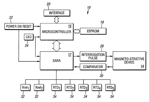
Figure 1 shows a typical structure of a sensor device generally 10 including a
sensor
advanced running period acquisition system (sometimes abbreviated as a SARA
system herein)
I2, a magnetostrictive sensing element I4, a microcontroller 16, an EEPROM 18,
an interface 20,
a power on reset 22, a C?tO 24, an interrogation pulse 26 passing from the
SARA system 12 to
the magnetostrictive device I4, a comparator 30 passing from the
magnetostrictive device 14 to
the SARA system 12, a set of temperature sensing reference devices 32, and a
plurality of
temperature sensing devices such as a resistive thermal device (sometimes
referred to as RTDs)
34.
As shown in Figure 2, the SARA system 12 includes a control unit 36 for
controlling
events and sequencing of devices communications. The SARA system I2 also
includes a high and
low cycle time, write only input registers 38a-b, a pulse length, write only
input register 40, a high
and low length, write only input registers 42s-b associated with a high noise
rejection (1-D~TR)
window, scale factor, write only input registers 44 and control, write only
input register 46.
The present method and device utilize a SARA system which includes a timing
system
having a fine clock that is an electronic circuit for measuring a short time
interval in conjunction
CA 02245884 2003-10-10
~06~~-3z
6
with a coarse clock for measuring a longer time interval. The values of these
two clocks are then
combined so that the coarse clock provides a whole number of counts and the
fine clock provides
the appropriate fraction of a whole number to yield a very accurate time
interval. The course
clock is a conventional clock such as a quartz clock, while the fine clock is
descn'bed in European
S published Application 050$232 as described fully herein.
Disclosure of European Published Application No 050$232
As shown in Figure 4, an electronic circuit for measuring a precise time
interval which is
present in the form of an electric measuring pulse comprises a ring osciDator
(OSC) which
comprises of a chain of series connected imreners (I3 - I16). A controllable
component consisting
of a NAND-gate (NA) and two additional inverters (I I, I2) switches the ring
oscillator (OSC) on
or oif, respectively. The complete clock periods thereof are counted in a
first pulse counter (Cl)
and a second pulse counter (C2). A phase indicator consisting of a storage
chain (SPK) and a
scoring logic (LOG) records the phase position of the last clock period of the
ring oscillator
(OSC) in the moment when the ring oscillator is switched off. On the basis of
the recorded phase
position, an arithmetic-logic unit (ALU) decides which of the two pulse
counters (CI) and (CZ)
contains the correct counting state and calculates the duration of the
measuring pulse from the
chosen counting state and the recorded phase position with a precision
corresponding to the
running time of an inverter.
One of the remarkable features of the circuit is an extremely high measuring
precision
around 200 pico seconds and this circuit can be inexpensively realized on a
single integrated
CMOS-switching circuit.
The invention relates to use of this electronic circuit for precisely
measuring the time
interval which is associated wish the reflection of an electric measuring
pulse, such as found with
a magnetostrictive effect.
It is common practice in measuring the reflection of a current pulse using
magnetostrictive
effects to design devices for measuring a time difference from the input pulse
to the output
CA 02245884 2003-10-10
70677-31
7
reflection as high-frequency counters or analogue circuits according to a
"Dual slope"-method.
If with this method short time intervals are to be measured with a high
precision, correspondingly
calibrated high counting frequencies are required in high-frequency counters.
A desired precision
of, e.g., 500 pico-seconds already requires a frequency of at least 2
gigahertz. Such calibrated
high frequencies, however, can only be realized with the most rapid ECL-
technologies, which is
connected with a corresponding constructive effort, for example for the
housing and for cooling,
and thus results in a very expensive device.
Thus, the object of the present invention is to provide a device for measuring
a time
difference from an input pulse to receipt of its effect which is, as regards
the circuit, designed
inexpensively and with which short time inten~als can be measured with high
precision.
This object may be achieved by the application of the principles disclosed in
the counter
of EPO 0508232 . This EPO application disclosed an electronic circuit
comprising wring
IS oscillator having a chain of series connected inverters, a controllable
Logic component which
switches the ring oscillator on or off in response to the measuring pulse
representing the time
interval, further at least one pulse counter which counts the number of the
complete clock periods
of the oscivating ring oscivator at one of the inverters, further a phase
indicator which records the
phase position of the ring oscillator in the moment when the ring oscillator
is switched off and
finally an arithmetic-logic unit connected with the pulse counter and the
phase indicator, which
outputs the measuring result as a multiple of the running time of an inverter
on the basis of the
recorded phase position and the counting state.
The core of the circuit is the controlled ring oscillator. This ring
oscillator is started with
the positive edge of the measuring pulse phased-synchronously to the measuring
pulse and then
oscillates with its own frequency which results from the running times of the
series connected
inverter steps as well as from their number.
The pulse counter counts the complete periods of the oscillating ring
oscillator as long as
the measuring pulse is applied. The trailing edge of the measuring pulse,
which corresponds to
CA 02245884 1998-08-13
WO 98/27401 PCTlUS96/20715
8
the end of the time interval to be measured, switches off the ring oscillator
via the controllable rt
logic component. The phase position of the last clock period in the moment of
the end of the
measuring pulse is recorded with the provided phase indicator. Thus, in the
pulse counter as well
as in the phase indicator there are provided all necessary information for
exactly determining the
duration of the measuring pulse or the time interval to be measured,
respectively, with a precision
corresponding to the running time of an inverter.
The measuring precision of the suggested electronic device for measuring a
time difference
is deterniined by the running time of the used inverters. In modern ASICs in
CMOS-technology
1~ today interval nlnning times around 200 pico-seconds are realizable without
any problems. Thus,
the measuring circuit is by far superior to common high-frequency counters;
moreover it can be
manufactured very inexpensively on one single chip. Another advantage is the
low current
consumption of the circuit.
In order to guarantee a safe dying of the oscillation of the ring oscillator,
the inverter chain
must not be too short as otherwise the amplitude of the ring oscillator does
not achieve the full
height in the &rst periods, which could also lead to incorrect counting states
in the pulse counters.
in the CMOS-technology here preferred, a NAND-gate presents itself as a logic
component for switching the ring oscillator on and off The running time of a
NAND-component
in the technology used here is approximately twice as long as the running time
of an inverter step.
Therefore, apart from the NAND-gate the controllable component comprises two
additional
inverters which subdivide the running time of the NAND-gate into two inverter
running times.
In a preferred embodiment, the ring oscillator comprises 14 inverters.
Together with the
two additional inverters at the NAND-component there are altogether 16 series
connected
inverter steps, which is a power of two, so that the subsequent logic
arithmetic operations are
simplified.
CA 02245884 1998-08-13
WO 98/27401 PCT/US96/207I5
9
r The switching off of the ring oscillator effected by the end of the
measuring pulse can be
effected in any phase position of its clock. If there is only one pulse
counter under unfavorable
~ conditions, the end ofthe measuring pulse could fall just on a counting
edge, and this would lead
to setup/hold-time-defects which in turn could lead to the counting state to
be incorrect. A fault
of 1 would for example mean a measuring inaccuracy of 32 inverter running
times when there are
altogether 16 inverter steps. In an advantageous development of the circuit,
there are therefore
two parallel pulse counters provided which are each operated time-shifted by
approximately half
a clock period. Thus, it is guaranteed that always at least one of the two
pulse counters is
deimedly switched off Which counter contains the correct counting state after
the ring oscillator
lU is switched offis decided by the arithmetic-logic unit on the basis of the
phase position of the ring
oscillator recorded in the phase indicator. However, the circuit basically
also works with only one
pulse counter.
In order to operate the two pulse counters with counting clocks which are each
time-
ZS shifted by half a clock period, they are preferredly connected with the
outputs of two subsequent
inverters.
A clock generator which is designed as a controllable divider precedes each of
the two
pulse counters. These clock generators have the function of converting the
period clock of the
20 ring oscillator which is sensed at the output of the respective inverter
step into a counting pulse
with a precisely known number of edges.
Preferably, the clock generators each comprise a flip-flop, the clock input of
which is
connected to the output of an inverter of the ring oscillator and the output
of which acts on the
25 input of the pertaining pulse counter, as well as a controllable inverter
at the input of which the
measuring pulse is applied and the output of which is connected to the data
input of the flip-flop.
An exclusive-or-component is used as controllable inverter which effects that.
At the output of
the flip-flop there is outputted a counting pulse with half a clock rate as
long as the measuring
pulse is applied at the input.
CA 02245884 1998-08-13
WO 98/27401 PCTlUS96/20715
The running times which inevitably occur due to the exclusive-or-component can
be
compensated by a hold-up line with a respective running time which is
preceding the clock input
of the flip-flop.
5 The phase indicator preferably comprises a storage chain and a scoring
logic. Here, the
storage chain comprises as many storage elements as there are inverters, each
storage element
being assigned to exactly one inverter and storing the logic condition thereof
at the moment when
the ring oscillator is switched off. The pertaining scoring logic compresses
the contents of the
storage chain to a figure representing the phase position of the last clock
period of the ring
10 oscillator and in addition collects the Logic condition of the first
storage element. In the chain of
storage elements the phase position of the last clock period of the ring
oscillator is recorded at
the moment when the ring oscillator is switched off by the trailing edge of
the measuring pulse.
On the basis of the thus "frozen up" last phase position and the logic value
of the first storage
element, it can be decided which of the two pulse counters contains the
correct counting state.
Particularly preferred is an embodiment in which the storage elements of the
storage chain
are D-flip-flops, the data inputs of which are connected with the outputs of
the pertaining
inverters and at the clock inputs of which the measuring pulse is applied.
When the circuit is designed as an integrated CMOS-switch circuit so-called
"matching
effects" can be utilized, as all logic function components present on the chip
have practically the
same dynamic behavior. This results in a further increase of the precision of
measurement or it
is a basic precondition for highly precise measurements.
The measuring circuit in Figure 6 designed as an integrated CMOS-circuit
substantially
consists ofa ring oscillator OSC, two pulse counters CI, C2 with pertaining
clock generators G1,
G2, a phase indicator consisting of a storage chain SPK and storage elements S
1 - S I 6 as well as
an arithmetic-logic unit ALU.
CA 02245884 1998-08-13
WO 98/27401 PCTlUS96/20715
11
The ring oscillator OSC is preceded by a NAND-gate NA as a controllable logic
component, the running time of which is subdivided into two inverters I1, I2.
At the input of the
NAND-gate NA the measuring pulse, the duration which is to be measured, is
applied. The
NAND-gate NA precedes the chain of 14 inverters i3 - I16 which are arranged in
series.
Two pulse counters C 1 and C2 are provided which are each preceded by a clock
generator
G1 or G2, respectively. The input of the clock generator G1 is connected with
the output of the
inverter I10, while the input of the second clock generator G2 is connected
with the output of the
subsequent inverter II 1.
The storage chain SPK comprises 16 equal storage elements S 1 - S 16 which are
here
designed as D-flip-flops, an inverter I 1 - I16 being assigned to each storage
element S 1 - S 16.
The clock generators G 1 and G2 preceding each of the pulse counters C 1 and
C2 each
contain a D-flip-flop FL and an exclusive-or-component EX according to Figure
5. The clock
input of the flip-flop FL is connected with the output of the corresponding
inverter I10 or I11,
respectively, ofthe ring oscillator OSC (cf. Figure 4}; its output Q directly
acts on the pertaining
pulse counter C 1 or C2, respectively, which commonly consists of a chain of
further D-flip-flops.
The exclusive-or component EX is used as a controllable inverter, the
measuring pulse
being applied to the one input A thereof, the other input B being connected to
the output Q of the
flip-flop FL, and the output of the inverter acts directly on the data input D
of the flip-flop FL.
For compensating the running time D1 on its way via the exclusive-or component
EX to the data
input D of the flip-flop FL, the clock input of the flip-flop FL is preceded
by a correspondingly
dimensioned hold-up line D2.
The measuring circuit works as follows:
With the rising edge of the measuring pulse, the duration of which is to be
exactly
determined, the ring oscillator OSC is started via the NAND-component NA phase-
CA 02245884 1998-08-13
WO 98/27401 PCT/LT596/20715
12
synchronously. The ring oscillator then oscillates with its own frequency
which results from the
running times of the inverters II - I16 as well as their number, until the
trailing edge of the
measuring pulse switches it off again. Figure 6 shows the clock periods of the
ring oscillator OSC
during the time interval TZ - T, which corresponds to the duration of the
measuring pulse.
As long as the ring oscillator OSC is oscillating, the complete clock periods
thereof are
counted by the pulse counters C1 and C2. In the process, the clock signals
tapped at the outputs
of the inverters I10 or I1 l, respectively, of the ring oscillator OSC are
converted into a counting
signal with half the number of pulses or with the double pulse width in the
preceding clock
generators G1 and G2. In the process, the running time DI of the measuring
pulse is
compensated up to the data input D of the flip-flop FL by the hold-up line D2
running in parallel
to the clock signal in such a way that the measuring pulse and the clock
signal arrive at the fiip-
flop FL phase-synchronously. The trailing edge of the measuring pulse switches
off the clock
generators G1 and G2 - and thus the connected pulse counters CI, C2.
1S
After the ring oscillator OSC is switched off in response to the negative edge
of the
measuring pulse, the present condition of the inverter chain, which represents
the phase position
of the last clock period, is transmitted to the storage elements S 1 - S 16 of
the storage chain SPK
which are assigned to each inverter I1 - I16. The scoring-logic LOG compresses
the contents of
the storage chain SPK to a five-bit-figure which indicates at which phase
position the ring
oscillator OSC was switched ofd
On the basis of the information about the phase position provided by the
scoring-logic
LOG, the arithmetic-logic unit ALU can now check which of the two pulse
counters C 1 and C2
has been switched offunder defined conditions. The arithmetic-logic unit ALU
finatIy calculates
from the counting state of the chosen pulse counters C 1 or C2, respectively,
and the recorded
phase position at the point of switching off the ring oscillator as well as
from the logic condition
of the first storage element S 1, the measuring result in the form of a figure
which indicates the
duration of the measuring pulse as a multiple of the running time of one of
the inverters I i - I16.
CA 02245884 1998-08-13
WO 98/27401 PCT/US9b/20715
I3
The duration of the time interval TZ - T2 thus determined up to a running time
of one
inverter between a rising and a trailing edge of the measuring pulse can
subsequently be further
processed.
As the running times of the inverters are not the same in every chip and are
moreover
subject to variations in temperature and voltage, it is necessary to carry out
calibrations before
the measuring circuit is initiated and when the measuring circuit is operated.
This can for example
be done by applying two measuring pulses of a known duration to the measuring
circuit and
obtaining a calibration curve by simple arithmetic, with the help of which the
later measuring
results can be converted into time differences. The arithmetic required for
doing this can be
realized by processors of a simple construction.
List of reference numerals:
OSC ring oscillator
NA NAND-gate
I1 - I16 inverters
C 1, C2 pulse counters
GI, G2 clock generators
FL flip-flop (of GI, G2)
D data input (of FL)
Q output (of FL)
EX exclusive-or-component (of
G1, G2)
A, B inputs (of EX)
Dl running time
D2 hold-up line
SPK storage chain
S I - S I 6 storage elements
LOG scoring logic
ALU arithmetic-logic unit
CA 02245884 1998-08-13
WO 98!27401 y'C'1'/(1896/20715
14
The basic principles of European Application 0508232A2 are in the SARA system
as
described and shown herein in connection with the timing system of the present
invention. The
timing system of the present invention uses a course conventional clock and a
fine clock as
described in this European Application incorporated above.
SARA System Operation
For measuring displacements of a measuring magnet of a magnetostrictive
device, the
SARA system 12 generates an interrogation or start pulse and receives a magnet
signal returning
from the magnetostrictive device 14. The magnet signal is compared in computer
30 to a
threshold voltage to form a stop pulse in SARA 12, as is well known in the
art. The SARA
system 12 then measures the time period between the start pulse and the stop
pulse in a time
measurement unit 48. The SARA system 12 then multiplies the time period by a
scale factor
stored in registers 44 and writes a result representing the time period to
four (4) 8-bit registers
so.
I5
Then, the SARA system 12 switches an INTO output 52 to its low state which
signals the
microcontroIler 16 that valid data is available for reading. The result
representing the time period
is then transferred to the p.C I6 in four (4) read cycles on one address. With
the transfer of the
last read cycle, the SARA system i2 clears an interrupt and is prepared to
receive additional
magnet signals to form the next stop pulse from the computer 30 (for mufti
magnet applications,
such as shown in U.S. Application Serial No.08/564,863, filed November 30,
1995, entitled
Magnetostrictive Position Sensing Probe with Waveguide Referenced to Tip, the
specification and
drawings of which are incorporated herein by reference). This procedure allows
a fast transfer
ofthe result into the uC 16. The p.C I6 then converts the transferred data
into a format that the
interface 20 needs (e.~ , converts the data into RS485 format).
All results can be and generally are corrected by reference measurements. The
unsealed
results are 28 bit wide, where the I 6 higher bits representing the number of
full MK clock periods,
the coarse clock, and the 12 lower bits representing a fraction of a full MK
clock period. Using
the recommended 4MHz for an MK clock, the least bit means or corresponds to a
61 ps (pico-
CA 02245884 1998-08-13
WO 98!27401 PCT/US96/20715
second) time period. The true resolution of the SARA system 12 of this
invention is typically
about 280 ps to about 180 ps, depending on temperature and supply voltage.
Only cyclic reading
for fast downloading of the results is also provided to permit the reading of
four registers 50 at
one address by using an internal counter to multiplex the address (calculated
from the original
5 data course and fine counters 51). All functions are controlled using
registers 38,40,42,44,46
which are connected to an 8-bit pC interface 54. The SARA system I2 offers two
modes for the
planed position and temperature measuring:
- everyone (the pC must be fast enough to read before new results come in)
which
10 can be as many as placed on the system.
- one addressable position (1 of 16) or 8 temperature ports for (RTD) port no.
(1
of 8)
15 The SARA system 12 is designed to be operated in a continuous measuring
mode. The
SARA system 12 is able to generate and transmit or send an interrogation pulse
having a
programmable length of up to 255 MK clock periods if the startout pin is
connected to the startin
pin. The SARA system 12 is also designed to operate in an external start mode
where the time
measurement will start either with the interrogation pulse or an incoming
pulse (ref. magnet)
either one coming from the startin pin disconnected from the startout pin.
Two 16 bit registers for programming a High Noise Rejection Window 42 a, 42b,
and
cycle time 38a, 38b. The window is a lower value, and will enable the stopin
after the internal
counter (internal to SARA) has counted out the cycle time 38a, 38b, has
reached the value of the
window 42 a, 42b and uC can adjust window 42a, 42b from one reading to the
next depending
on the location of the magnets) in the magnetostrictive device. Every
measurement includes a
scaling 44 with a 24 bit value, made by the internal high speed ALU (internal
to SARA).
Interrupts 52 and one bit change in the status register 53 will be generated
when new results are
available. The cycle time 38a, 38b is reached or an overflow (temperature
measurement only for
CA 02245884 1998-08-13
WO 98J27401 PCT/CTS96/20715
16
fixed high value) error occurs. Interrupts will be cleared by reading the
result register 50 four
times, or the interrupt clear register through I/O port 54.
The SARA system 12 includes a control unit 36 which is a state machine
programmed for
the desired sequence of events as necessary to operate the particular
magnetostrictive position
sensor 14, reads the discharging times for temperature and processes a result
from those
measurements. The 8 bit control register 46 stores control information that
comes in from a bus
54. The 8 bit length register 40 stores the desired pulse width of the
interrogation pulse. The
cycle time high and low registers 38a-b store 16 bit information for the rate
at which the
interrogation sequence repeats. The high and low HNR (high noise rejection)
registers 42a-b
store 16 bit information for a time window around the expected termination of
the measured time
interval. Any pulses occurring outside of the window are rejected as described
more fully in
United States Patent No. 4,721,902.
The I/O interface bus, or port, 54 is a uController interface, preferably
based on the Intel
pC family of controller interfaces, available from the Intel Corporation. It
is used for bi-
directional communication with an external microprocessor (not shown) as
needed. The time
measurement unit 48 determines a 28 bit result stored in the result registers
50 for the magnet
position from the duration of the time period between the start pulse and the
stop pulse. If the
scale factor is 1.0, then the 16 higher bits of the result are the count of
full periods of an internal
(or external) crystal controlled coarse clock 56 such as MK clock which
determines a coarse
count. The I2 lower bits of the result are derived from a pulsed (oscillator)
ring counter or fine
clock 58 of a type described above which determines a fine count. The time
measurement unit
48 also includes three 8 bit registers 44 to store the 24 bit scaling factor.
The scaling factor is used to determine the number of inches (centimeters) a
bit represents,
e.g., assume the crystal clock operates at 2 MHz, the speed of sound in the
waveguide is 9.05125
us per inch, and an output scaling of 0.013487 inches per bit is desired, then
the scaling factor
would be O1B9EDh which would mean that a measurement count of 000186AOh would
be stored
as 100.000 inches after scaling.
CA 02245884 2003-10-10
70677-31
17
The resuh registers 50 comprise four 8 bit registers which are used to store
the total count
which represents the magnet position.
The pController 54 also contn'butes to the measuring efficiency of the SARA by
varying
the threshold voltage of the comparator 30 so that the signal from the sending
element (distant
magnet) is maintained at an easily measured value. The lrController 54
performs this task by
using an SPOT (electron potentiometer) 60 to vary the voltage as the magnet or
sending element
gets further away from the source. Additionally, the SPOT control mechanism
can be used to
vary the signal with time and to adjust and maintain the signal strength.
The lrController 54 may include an SPOT with control logic that controls the
SPOT as
executed by the Controller as shown in U.S. Patent 5,640,109, entitled Pulse
Detector by
David Nyce.
Additionally as shown in Figure 2, temperature measurements are determined by
a
temperature measurement unit 62 which uses the time measurement unit 48 and
resulting time
period to determine the temperature of the RTD 34. The temperature measurement
unit 62 is
detailed in figure 3, which shows that temperature measurement unit 62
includes a capacitor Co
64 which is discharged over the temperature sensing RTDs 34, an SNS or a
Schmitt trigger input
66 which is connected to the capacitor 64, and a transitor 68. When the
voltage reaches the
threshold voltage of the SNS input 66, the time measurement is stopped and a
CHA output 70
switches from high impedance to low, so that the capacitor 64 is recharged.
The discharge time or time period to be measured depends on the resistance of
each RTD
34 and switching transistors 68, a supply voltage, the capacitor 64 and the
threshold voltage of
the SNS input 66. By using reference resistors 32, 78, it is possible to
eliminate these influences
(except the influence of the RTD). The SARA system 12 measures the time
between start and
stop pulses, or for discharging a capacitor to a threshold voltage.
CA 02245884 1998-08-13
WO 98/27401 PCT/US96/20715
18
The temperature measurement unit 62 as shown in Figure 3 translates a
resistance into a
time period. This allows measurement of the RTDs 34 or other resistances. In
operation, the
charge or CHA pin 68 charges up the measurement capacitor Co 64 to the power
supply voltage.
Then, the charge pin 68 will disconnect. A port Po 72 turns on a transistor Q
R~f 68 through a
current limiter R~~f 74 and a speed up capacitor Cue. 76. This discharges the
capacitor Co 64
through the resistor R~ 78 to be measured. The sense or SNS pin 66 senses when
the capacitor
Cfl 64 becomes discharged to a certain threshold voltage. The time period
between turning on the
port PQ 72 and when the capacitor Co 64 is discharged is the time period that
proportional to the
resistance of the resistor Ran 78. This time period is stored, and the same
operation is repeated
for each resistance to be measured, e.~, a port P, 72a, a resistor R, 74a, a
speed up capacitor C,
76a, a transistor Ql 68a, are used to measure a resistance of a resistor R
lmp, 78a, etc. The
resulting time periods are measured in the same way as described for Figure 2
for measurement
of the position magnet. When all the measurements are completed, the
temperature measurements
(R~."~1 through RT",~) are scaled by the measurement of the resistor RR~f 74.
The resistor RR~f 74
is a precision resistor with a very low temperature coe~cient and is used as a
resistance reference.
The SARA system 12 was developed for measuring running periods and discharging
times
to calculate levels and temperatures, e.g., ASIC. The SARA system I2 is a CMOS-
Sea-of-Gates-
Chip, and runs on 3.3 volts. To reach the highest possible accuracy, the SARA
system 12 needs
a big buffer capacity on every supply pin (CX61-CX64).
As stated above, temperatures are determined by a resistance relation
calculation based
on the discharging times of reference resistors and a Pt1000 80 (RTD Platinum
'I000 Ohms). As
described above, a capacitor is charged by a charge or CHA output 70 and
switches the CHA
output 70 off (high impedance) and a port output to become high, so that the
capacitor is
discharged over a resistor and a transistor. Inside the SARA system 12 the
time measurement is
started. If the voltage ~of a capacitor reaches the threshold voltage of a
schmitt-trigger or SNS
input 66 (or the external comparator 30 which is connected to the SNS input
66), the time
measurement is stopped and the CHA output becomes high again to charge the
capacitor for the
next measurement. The SARA system 12 has two modes for the temperature
measurement:
CA 02245884 1998-08-13
WO 98/27401 PCT/LTS96/20715
19
- the discharge time of one resistor (port) is measured
- the discharge time of port 0 up to port x is measured one after the other
To calculate the unknown resistor (Rtmp), the value of the reference resistor
is multiplied
by the ratio of the discharge times of Rtmp and Rref.
To have a higher accuracy, the following algorithm to calculate the
temperature is used:
The multiple mode is used to measure the discharge times of port 0 up to port
6. The discharge
times of 256 of such measurements are added, so that for each port a sum of
256 measurements
is stored in the pController. Two ports measure reference resistors, the other
ports are for the
RTDs (Pt1000), which have a resistance of ca. 1000 iZ at 0°. The
reference resistors have known
resistances of 1000 S2 and 2000 ~2. The difference of the sums of Rref2 and
Rrefl (Sdiff = Sret2 -
Srefl) is used as a 1000 ~2 reference. Because of delay times, for example,
the time to switch the
transistor Q1, contain all values and offset Toff'. The transient offset Toff
is measured every
measurement so that the delay time can ultimately be factored out of the
measured time. By
calculating the difference Sdii~ the oi~'set Toff is dropped. The sum of the
1000 ~2 resistor Srefl
contains the offset, so that the offset itself can be calculated with Toff =
Srefl - Sdiff. Toff is
subtracted from all sums of the RTDs. These corrected sums are linear to the
resistors of the
RTDs. To obtain their resistance they are divided by the 1000 S2 reference
Sdiff. The resistance
of a Pt1000 is almost linear to the temperature, so that a linear equation can
be used to calculate
the temperature from the resistance. The delay time Toff is not exactly the
same time for each
port. To eliminate this error, the delay time can be determined individually
for every port and then
stored in the EEPROM to use it for the calculation.
The resistance of the Pt1000 is not exactly linear to the temperature, and
they have
_ variations from piece to piece in the absolute resistance, but they have the
same temperature
coe~cient. This can also be considered in the calculations, by adjusting for
the slight nonlinearity,
as shown in reference manuals for Pt1000.
CA 02245884 1998-08-13
WO 98127401 PCT/US96/20715
Thus, the SARA system 12 yields a method to increase the resolution of
measurement of
a time period for a given frequency of precision oscillator in a position
sensor, without requiring
averaging or summing of several time periods to obtain said increased
resolution. It includes:
5 a precision oscillator first means for providing a coarse count for the more
significant bits
of the time measurement,
a high frequency oscillator second means for providing a fine count for the
less significant
bits of the time measurement,
1~
a register for storing coarse and fine counts from said first and second
means, said register
containing the complete high resolution measurement of the time period
representing the
position measurement or other measurement by time for use to determine the
value of a
physical variable such as time or resistance.
The precision oscillator is crystal controlled. The high frequency oscillator
may be a ring
oscillator.
A complete set of coarse and fine counts is obtained as the result of
supplying as few as
one excitation pulse to the waveguide.
The interrogation pulse for excitation of the waveguide has a programmable
length. For
measuring resistance in conjunction with a position sensor, the charging of a
capacitor, the
measuring of the time required to discharge to a threshold voltage said
capacitor and control
circuitry to cause said charge and discharge to occur is used and the
resistance to be measured
changes in response to temperature changes, and this change in resistance is
used to measure
temperature.
Control circuitry is used to multiplex among more than one resistance to be
measured, and
at least one of such resistances is a stable resistance for use as a
calibration reference.
CA 02245884 1998-08-13
WO 98/27401 PCT/US96/20715
21
For position sensing, a raw count represents the position measured and storing
also a
scaling factor for scaling the raw count to desired units.
k
The sensor for position sensing also has a window in time surrounding the time
during
which a return pulse is expected to arrive, said window defining a time period
outside of which
signals will not be accepted by the receiving circuitry, said window timing
derived by using the
contents of a coarse count register and subtracting the desired number of
counts.
Although the invention has been described in conjunction with specific
embodiments, it
is evident that many alternatives and variations will be apparent to those
skilled in the art in light
of the foregoing description. Accordingly, the invention is intended to
embrace all of the
alternatives and variations that fall within the spirit and scope of the
appended claims.