Language selection

Search

Patent 2245965 Summary

Third-party information liability

Some of the information on this Web page has been provided by external sources. The Government of Canada is not responsible for the accuracy, reliability or currency of the information supplied by external sources. Users wishing to rely upon this information should consult directly with the source of the information. Content provided by external sources is not subject to official languages, privacy and accessibility requirements.

Claims and Abstract availability

Any discrepancies in the text and image of the Claims and Abstract are due to differing posting times. Text of the Claims and Abstract are posted:

  • At the time the application is open to public inspection;
  • At the time of issue of the patent (grant).
(12) Patent: (11) CA 2245965
(54) English Title: MINIATURE CARD EDGE CLIP
(54) French Title: PINCE LATERALE POUR CARTE MINIATURE
Status: Deemed expired
Bibliographic Data
(51) International Patent Classification (IPC):
  • H01R 4/26 (2006.01)
  • H01R 4/64 (2006.01)
  • H01R 4/66 (2006.01)
  • H01R 13/648 (2006.01)
  • H01R 12/04 (2006.01)
  • H01R 12/18 (2006.01)
  • H01R 12/32 (2006.01)
(72) Inventors :
  • DELPRETE, STEPHEN D. (United States of America)
  • BARNUM, DAVID M. (United States of America)
  • SOUSA, LUIS A. (United States of America)
(73) Owners :
  • THOMAS & BETTS INTERNATIONAL, INC. (United States of America)
(71) Applicants :
  • THOMAS & BETTS INTERNATIONAL, INC. (United States of America)
(74) Agent: MACRAE & CO.
(74) Associate agent:
(45) Issued: 2001-12-18
(86) PCT Filing Date: 1997-12-22
(87) Open to Public Inspection: 1998-07-02
Examination requested: 1998-08-12
Availability of licence: N/A
(25) Language of filing: English

Patent Cooperation Treaty (PCT): Yes
(86) PCT Filing Number: PCT/US1997/023422
(87) International Publication Number: WO1998/028818
(85) National Entry: 1998-08-12

(30) Application Priority Data:
Application No. Country/Territory Date
08/771,978 United States of America 1996-12-23

Abstracts

English Abstract


An edge clip is disclosed for electrically connecting
a conductive pad on the surface of a printed circuit board
or its edge to an external connector. The edge clip (10)
is substantially U-shaped, with first and second opposing,
non-parallel sides (12, 14) defining a space therebetween.
For connection, the printed circuit board edge is fitted into
the space such that the opposing sides provide spring-like
deflective force against the pad and the printed circuit board
(38), thereby providing a more reliable connection. The edge
clip may include an alignment feature for facilitating alignment
prior to soldering. The alignment feature may include small
projections formed on the edge clip to align with, and fit into,
holes on the printed circuit board. Scored sections (28) may
be disposed on one edge of the clip to facilitate removal of
the edge clip from a carrier during assembly. Further, the
edge clip may include a center beam (54) extending away
from one of the opposing surfaces to provide contact with
another metallic surface, such as a miniature card case, thereby
providing additional grounding capabilities which can provide
protection against static discharge.


French Abstract

La présente invention concerne une pince latérale destinée à connecter électriquement une plage conductrice placée sur la surface d'une carte à circuit imprimé ou le bord de cette dernière à un connecteur externe. La pince latérale (10) de la présente invention présente une forme essentiellement en U, un premier et un deuxième côté (12, 14) opposés et non parallèles définissant un espace entre eux. Pour établir la connexion, on introduit le bord de la carte à circuit imprimé dans cet espace de manière que les côtés opposés exercent une force de déviation du type ressort contre la plage conductrice et la carte à circuit imprimé (38), assurant de cette manière une connexion plus fiable. La pince latérale peut comprendre un élément d'alignement permettant de faciliter l'alignement avant la soudure. L'élément d'alignement peut être constitué de petites projections formées sur la pince latérale, lesquelles projections s'alignent avec les trous de la carte à circuit imprimé dans lesquels elles s'introduisent. Des pré-rainures (28) peuvent être formées sur un bord de la pince afin de faciliter la séparation de la pince latérale et d'un support du pince au cours de l'assemblage. La pince latérale peut en outre comprendre une patte centrale (54) s'étendant depuis l'une des surfaces opposées afin d'établir le contact avec une autre surface métallique, telle qu'un boîtier de carte miniature, ce qui permet de multiplier les fonctionnalités de mise à la masse pouvant assurer une protection contre les décharges d'électricité statique.

Claims

Note: Claims are shown in the official language in which they were submitted.


-8-
CLAIMS
1. An edge clip for electrically connecting a conductive pad
disposed on a printed circuit board surface to an external
contact proximate to the printed circuit board edge, the printed
circuit board having a predetermined thickness dimension,
comprising:
a first planar member formed from a resilient conductive
material;
a second planar member connected to said first planar member
by a connecting member, said first and second planar members
being non-parallel and defining a space therebetween which
decreases from a point adjacent said connecting member to a point
at ends of said first and second planar members which are distal
from said connecting member, said space defined between the ends
of said planar members in an undeflected state being less than
the thickness of the printed circuit board,
first and second legs extending from said first planar
member to respective end; and
a center beam which extends angularly away from said first
planar member;
whereby, for connection purposes, the printed circuit board
is fitted into said space such that said first and second planar
members provide spring-like deflective force against the pad and
the printed circuit board, thereby providing a more reliable
connection, and further whereby said connecting member disposed
between said first and second planar members can be placed in
electrical connection with at least one external contact in order
to provide connectivity between the pad and the at least one
external contact.
2. The edge clip of claim 1 further including first and second
scored sections disposed at the ends of said first and second
legs, respectively.
3. The edge clip of claim 2 further including first and second


-9-
protrusions disposed on said first and second legs, respectively,
said protrusions formed to interlock with holes disposed in the
printed circuit board.
4. The edge clip of claim 1 wherein said first and second
planar members have different length dimensions, said first
planar member having a longer length dimension than said second
planar member.
5. The edge clip of claim 1 wherein said first and second
planar members have different length dimensions, said second
planar member having a longer length dimension than said first
planar member.
6. The edge clip of claim 1 wherein said edge clip is formed
from a copper alloy having a thickness which exhibits both
flexibility and resiliency, whereby said planar members can be
deflected.
7. The edge clip of claim 1 wherein said edge clip is stamped
from a plated copper sheet.
8. An edge clip for electrically connecting a conductive pad
disposed on a printed circuit board surface to an external
contact proximate to the edge of the printed circuit board, the
printed circuit board having a plurality of alignment holes and
a predetermined thickness dimension, comprising:
a first planar member formed from a resilient conductive
material;
first and second legs extending from said first planar
member to respective ends thereof, said first and second legs
including first and second scored sections disposed at ends of
said first and second legs, respectively, said first and second
legs including first and second protrusions disposed thereon,
respectively, such that said protrusions interlock with the


-10-
alignment holes disposed in the printed circuit board;
a second planar member connected to said first planar member
by a connecting member, said second planar member having a
smaller length dimension than said first planar member, said
first and second planar members being non-parallel and defining
a space therebetween which decreases from a point adjacent said
connecting member to a point at ends of said first and second
planar members which are distal from said connecting member, said
space defined between ends of said planar members in an
undeflected state being less than the thickness of the printed
circuit board; and
a center beam which extends angularly away from said first
planar member to provide electrical contact with a feature other
than the printed circuit board pad and the external contact,
whereby, for connection purposes, the printed circuit board
is fitted into said space such that said first and second planar
members provide spring-like deflective force against the pad and
the printed circuit board, thereby providing a more reliable
connection, and further whereby said connecting member disposed
between said first and second planar members can be placed in
electrical connection with the external contact in order to
provide connectivity between the pad and the external contact.
9. A vertically installed edge clip for use with a printed
circuit board having an edge and a surface portion, at least two
locating holes of predetermined diameter being formed in the
surface portion, consisting of:
a planar body section having first and second distal ends;
a planar edge section disposed on said first distal end of
said planar body section, said planar edge section offset at a
predetermined angle relative to said planar body section;
at least first and second lead sections disposed on said
second distal end of said planar body section, said at least
first and second lead sections offset at a predetermined angle


-11-
relative to said planar body section,
said edge clip being vertically mounted on the printed
circuit board by inserting said at least first and second lead
sections in the at least two locating holes in the surface
portion of the printed circuit board such that said planar edge
section is proximate to the edge of the printed circuit board,
said at least first and second lead sections facilitating
maintaining proper alignment of said edge clip with respect to
the printed circuit board.
10. The edge clip of claim 9 wherein said first and second lead
sections are arranged approximately perpendicular to said planar
body section.
11. The edge clip of claim 10 wherein said first and second lead
sections decrease in width at respective distal portions thereof.
12. The edge clip of claim 10 wherein said planar edge, section
is approximately perpendicular to said planar body section.
13. The edge clip of claim 12 wherein said first and second lead
sections are secured to the printed circuit board by solder.
14. The edge clip of claim 12 wherein the printed circuit board
includes a conductive pad disposed on the surface thereof between
at least one of said locating holes and the edge, and said planar
body section is adhered to the conductive pad by solder.
15. The edge clip of claim 12 wherein said edge clip is stamped
from a plated copper sheet.
16. The edge clip of claim 9 having at least one planar surface
which can be held by a suction device of a pick and place machine
for surface mount installation.

Description

Note: Descriptions are shown in the official language in which they were submitted.


CA 02245965 1998-08-13
WO 98/28818 PCT/US97/23422
-1-
TITLE OF THE TNVENTION
MINIATURE CARD EDGE CLIP
CROSS REFERENCE TO RELATED APPLICATIONS
Not Applicable
STATEMENT REGARDING FEDERALLY SPONSORED
RESEARCH OR DEVELOPMENT
Not Applicable
BACKGROUND OF THE INVENTION
The use of removable, self-contained electronic devices
such as memory cards designed according to the MCIF
Specification is known. Such devices offer advantages
because of their relatively convenient size, typical plug and
play compatibility and ease of removal, among other things.
However, these advantages are dependent upon providing
reliable electrical connection between the removable device
and the host device. It is therefore desirable to have
small, reliable connectors for interfacing such removable
devices and host devices.
BRIEF SUMMARY OF THE INVENTION
An edge clip is disclosed for providing an electrical
pathway between a conductive pad on the surface of a
miniature card printed circuit board and an external
connector proximate to the edge of the printed circuit board.
The edge clip includes first and second opposing, non-
parallel, planar members defining a space therebetween. For
connection purposes, the printed circuit board is fitted into
the space. The opposing sides then provide spring-like
deflective force against the pad and the printed circuit


CA 02245965 1998-08-13
WO 98/28818 PCT/US97/23422
-2-
board, thereby providing a more reliable connection. The


planar members provide spring-like deflective force against


the pad and printed circuit board because, in an undeflected


state, the space defined between the opposing members is less


than the thickness of the printed circuit board. In order


to secure the edge clip in place more permanently the clip


may subsequently be soldered to the pad. A connecting member


disposed between the first and second opposing members is


then placed in electrical connection with an external


connector in order to provide connectivity between the


printed circuit board an external device.


The edge clip may also include an alignment feature for


facilitating alignment of the edge clip with respect to the


printed circuit board pad. The alignment feature is an


interlocking protrusion and recess. While the protrusion may


be formed on either the printed circuit board or the edge


clip, in the preferred embodiment the protrusion is formed


on the malleable legs of the edge clip by bending or stamping


to provide bumps which will align with the corresponding


holes formed in the printed circuit board.


The edge clip may also include a center beam which


extends away from the clip to provide electrical contact with


a feature other than the printed circuit board pad and the


external contact . For example, a center beam can be employed


to deflect against a miniature card metal housing to provide


protection against damaging static discharge.


Alternatively, the edge clip may include a planar body


section having location leads and a planar edge section


extending respectively from distal ends thereof. The planar


edge section and the body section are approximately


perpendicular and are connected by a rounded edge. The leads


and the body section are also approximately perpendicular and


connected by a rounded edge. The location leads facilitate


positioning the edge clip on a printed circuit board. More


particularly, position locating holes are drilled in the


printed circuit board prior to installation of the edge clip


- CA 02245965 1998-08-13
WO 98/28818 PCT/US97/23422
-3-
and the edge clip is mounted on the printed circuit board by
inserting the leads into the locating holes such that the
planar edge section is proximate to the edge of the printed
circuit board. The edge clip can then be more securely
attached to the printed circuit board by means such as
soldering.
BRIEF DESCRIPTION OF THE SEVERAL VIEWS OF THE DRAWING
l0 The present invention will be more fully understood from
the following detailed description of the drawing, in which:
Fig. 1 is a perspective view of a miniature card edge
clip;
Fig. 2 is a top view of the edge clip of Fig. 1;
Fig. 3 is a side view of the edge clip of Fig. 1;
Fig. 4 is a front view of the edge clip of Fig. 1;
Fig. 5 is a perspective view of an alternative
embodiment of the edge clip;
Fig. 6 is a top view of the edge clip of Fig. 5;
Fig. 7 is a side view of the edge clip of Fig. 5;
Fig. 8 is a front view of the edge clip of Fig. 5;
Fig. 9 is a side view of the edge clip of Fig. 1
connected to a printed circuit board;
Fig. 10 is a partially cut away side view of the edge
clip of Fig. 9 disposed in miniature card;
Figs. 11 and 12 are perspective views of a second
alternative edge clip;
Fig. 13 is a bottom view of the second alternative edge
clip;
Fig. 14 is a side view of the second alternative edge
clip; and
Fig. 15 is a perspective view illustrating installation
of the second alternative edge clip on a printed circuit
board.


CA 02245965 1998-08-13
WO 98/28818 PCT/ITS97/23422
-4-
DETAILED DESCRIPTION OF THE INVENTION


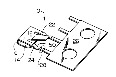
Referring now to Figs. 1-4, a U-shaped edge clip 10


suitable for use in conjunction with a miniature card printed


circuit board is illustrated. The edge clip includes a first


planar member 12 and a second planar member 14 which are


joined by a connecting member 16. The first and second


planer members are non-parallel, defining a space 18


therebetween. More particularly, the planar members are


offset by from 5-15 degrees, and the space defined


therebetween is greatest adjacent the connecting member,


decreasing toward an end 20 distal to the connecting member.


The edge clip also includes first and second legs 22,


24 which extend from the first planar member. More


particularly, the first and second legs extend from opposite


sides of the first planar member and, prior to installation


of the edge clip on a printed circuit board, are connected


to a clip carrier 26. In order to facilitate removal of the


edge clip from the clip carrier, a scored breakaway section


28 is formed at the interface between the edge clip and the


clip carrier such that the edge clip easily breaks away from


the clip carrier at the scored section when the edge clip and


carrier are bendably moved relative to one-another.


Referring now to Figs. 5-8, in an alternative embodiment


the edge clip includes upper and lower planar members 30, 32


which are connected by a connecting member 34. The upper and


lower planar members are non-parallel and define a space 36


therebetween which decreases from the cross member to the


distal end of the lower planar member. As such, the edge


clip squeezably deflects against the edge of a printed


circuit board when mounted thereto, and tends to remain in


a fixed position prior to soldering thereto.


Referring now to Figs. 3, 7, 9 and 10, for connection


purposes the printed circuit board 38 is fitted into the


space defined between the opposing members. In an


undeflected state, i.e., before fitting to the printed


circuit board, the space defined between the opposing members


CA 02245965 2001-02-O1
-5-
is less than the thickness 40 of the printed circuit board. The
edge clip is preferably manufactured from a copper alloy having a
thickness which exhibits both flexibility and resiliency. The
edge clip could also be ,tamped from a plated copper sheet. The
planar members thus provide spring-like deflective force against
the pad and printed circuit board when fitted thereto. In order
to secure the edge clip in place more permanently the clip may
subsequently be soldered to the pad 42.
The first and second planar members have different length
dimensions in order to facilitate installation of the edge clip
on the printed circuit board. In particular, the first planar
member 12 is longer than the second planar member 14, thereby
allowing the distal end 20 to be butted against the lower surface
of the printed circuit board, after which the edge clip is
rotated until the edge enters the space 18. Such a feature is
useful if the space 18 at: the distal end 20 is less than the
thickness of the printed circuit board, since it can be difficult
to press the edge clip st:raight onto the printed circuit board
edge.
When the printed circuit board is installed in a miniature
card housing 44, the connecting member disposed between the first
and second opposing members can be placed in electrical
connection with an external connector 46 in order to provide
connectivity between the printed circuit board and external
device 48. More particularly, as the miniature card is inserted

CA 02245965 2001-02-O1
- Sa -
into a host device the edge clip contacts the external connector,
which deflects to provide secure and reliable connection.
As shown in Figs. 1-4, 9 and 10, the edge clip may also
include alignment features for facilitating alignment of the edge
clip with respect to the printed circuit board pad. Each
alignment feature is an :interlocking protrusion 50 and recess 52
which are configured to align and securely interlock. While the
protrusion may be formed on either the printed circuit board or
the edge clip, in the preferred embodiment the protrusion is
formed on the metal edge clip


CA 02245965 1998-08-13
WO 98/28818 PCT/US97/23422
-6-
legs by bending or stamping to provide bumps which will align


with the corresponding holes drilled in the printed circuit


board.


The edge clip may also include a center beam 54 which


extends away from the clip to provide electrical contact with


a feature other than the printed circuit board pad and the


external contact. For example, the center beam can be


employed to deflect against a conductive miniature card


housing to provide protection against damaging static


discharge. The center beam extends angularly upward from the


first planar member in order to provide such connection.


More particularly, the center beam extends at an angle


relative to the first planar member which will allow


deflection against the conductive housing.


A second, surface mountable alternative embodiment of


the edge clip is illustrated in Figs. 11-15. The second


alternative edge clip includes a planar body section 60


having a planar edge section 62 and two location leads 64


extending from distal ends thereof. The planar edge section


62 and the body section 60 are approximately perpendicular


and are connected by a rounded edge. The leads 64 and the


body section 60 are also approximately perpendicular and


connected by a rounded edge. Each lead 64 includes a width


dimension that decreases at a portion of the lead distal from


the body section 60.


The location leads 64 facilitate positioning the edge


clip on a printed circuit board 66 for surface mount type


installation. More particularly, position locating holes 68


are drilled in the printed circuit board 66 prior to


installation of the edge clip. The edge clip is then mounted


vertically on the printed circuit board such that the


location leads 64 are inserted into the locating holes 68,


the body section 60 is parallel to the surface 70 of the


printed circuit board, and the planar edge section 62 is


proximate to the edge 72 of the printed circuit board.


vertical mounting allows use of a "pick and place" machine


CA 02245965 1998-08-13
WO 98/28818 PCT/US97/23422
_7_
for installation. For example, a layer of paste may be
placed on pad 64 and the pick and place machine can put the
edge clip in place on the paste for soldering. The edge clip
is then connected to the printed circuit board by soldering
means such as infrared reflow. The alignment leads 64
maintain edge 62 in position relative to the edge of the
printed circuit board during reflow.
In order to connect the edge clip to the printed circuit
board, the holes 68 may be plated through such that the
location leads are soldered to the printed circuit board.
Such connection may also optionally serve to electrically
connect the edge clip to components mounted on the printed
circuit board. Alternatively, a conductive pad 74 may be
disposed on the surface of the printed circuit board
proximate to the location leads 64 and body section 60. The
body section and/or lead may then be soldered to the pad.
Other alternative embodiments and modifications of the
above described edge clip will be apparent to those of skill
in the art. It will therefore be appreciated that the
present invention is not to be viewed as limited to the
specific embodiments described herein, but rather should be
viewed as limited only by the spirit and scope of the
appended claims.

Representative Drawing
A single figure which represents the drawing illustrating the invention.
Administrative Status

For a clearer understanding of the status of the application/patent presented on this page, the site Disclaimer , as well as the definitions for Patent , Administrative Status , Maintenance Fee  and Payment History  should be consulted.

Administrative Status

Title Date
Forecasted Issue Date 2001-12-18
(86) PCT Filing Date 1997-12-22
(87) PCT Publication Date 1998-07-02
(85) National Entry 1998-08-12
Examination Requested 1998-08-12
(45) Issued 2001-12-18
Deemed Expired 2012-12-24

Abandonment History

There is no abandonment history.

Payment History

Fee Type Anniversary Year Due Date Amount Paid Paid Date
Request for Examination $400.00 1998-08-12
Application Fee $300.00 1998-08-12
Registration of a document - section 124 $50.00 1999-04-28
Maintenance Fee - Application - New Act 2 1999-12-22 $100.00 1999-12-03
Maintenance Fee - Application - New Act 3 2000-12-22 $100.00 2000-09-27
Final Fee $300.00 2001-08-21
Maintenance Fee - Application - New Act 4 2001-12-24 $100.00 2001-09-27
Maintenance Fee - Patent - New Act 5 2002-12-23 $150.00 2002-11-04
Maintenance Fee - Patent - New Act 6 2003-12-22 $150.00 2003-11-05
Maintenance Fee - Patent - New Act 7 2004-12-22 $200.00 2004-11-04
Maintenance Fee - Patent - New Act 8 2005-12-22 $200.00 2005-12-02
Maintenance Fee - Patent - New Act 9 2006-12-22 $200.00 2006-11-30
Maintenance Fee - Patent - New Act 10 2007-12-24 $250.00 2007-11-30
Maintenance Fee - Patent - New Act 11 2008-12-22 $250.00 2008-12-01
Maintenance Fee - Patent - New Act 12 2009-12-22 $250.00 2009-12-01
Maintenance Fee - Patent - New Act 13 2010-12-22 $250.00 2010-11-30
Owners on Record

Note: Records showing the ownership history in alphabetical order.

Current Owners on Record
THOMAS & BETTS INTERNATIONAL, INC.
Past Owners on Record
AUGAT INC.
BARNUM, DAVID M.
DELPRETE, STEPHEN D.
SOUSA, LUIS A.
Past Owners that do not appear in the "Owners on Record" listing will appear in other documentation within the application.
Documents

To view selected files, please enter reCAPTCHA code :


To view images, click a link in the Document Description column. To download the documents, select one or more checkboxes in the first column and then click the "Download Selected in PDF format (Zip Archive)" or the "Download Selected as Single PDF" button.

List of published and non-published patent-specific documents on the CPD .

If you have any difficulty accessing content, you can call the Client Service Centre at 1-866-997-1936 or send them an e-mail at CIPO Client Service Centre.


Document
Description 
Date
(yyyy-mm-dd) 
Number of pages   Size of Image (KB) 
Claims 2001-02-01 4 179
Representative Drawing 2001-11-14 1 10
Cover Page 2001-11-14 1 48
Abstract 1998-08-12 1 55
Description 1998-08-12 7 339
Claims 1998-08-12 5 203
Drawings 1998-08-12 5 71
Cover Page 1998-10-29 2 75
Abstract 1998-08-13 1 58
Description 1998-08-13 7 339
Claims 1998-08-13 5 206
Drawings 1998-08-13 4 76
Description 2001-02-01 8 336
Representative Drawing 1998-10-29 1 4
Assignment 1999-04-28 1 40
Prosecution-Amendment 2001-02-01 8 286
Correspondence 2001-08-21 1 33
Correspondence 1999-07-20 1 1
Assignment 1999-06-25 2 52
Assignment 1998-08-12 10 309
PCT 1998-08-12 3 117
Correspondence 1998-10-27 1 32
PCT 1998-08-13 2 79
Prosecution-Amendment 2000-10-03 1 29