Note: Descriptions are shown in the official language in which they were submitted.
CA 02246084 1998-08-28
1
METHOD OF PATTERNING SEMICONDUCTOR MATERIALS AND OTHER
BRITTLE MATERIALS
RELATED APPLICATION
This application is related to a Canadian patent
application serial no. entitled "Method of
cleaving a semiconductor wafer" to T. Simpson et al., filed
concurrently herewith and incorporated here by reference.
FIELD OF THE INVENTION
This invention relates to a method of patterning
brittle materials, and in particular to a method of
patterning semiconductor materials.
BACKGROUND OF THE INVENTION
Patterning of the materials used in the semiconductor
industry is one of the major steps in fabrication of
microelectronic devices, integrated circuits and
optoelectronic devices including semiconductor lasers.
Conventionally known methods of patterning comprise
selectively masking a semiconductor material with a
photoresist or any other masking material, followed by
etching. Known etching methods include selective wet
chemical etching, or dry etching, e.g. plasma and reactive
ion etching. (E. g. see Van Nostrand's Scientific
Encyclopedia, 7th Edition, Ed. by Douglas and Glenn
Considine, NY, 1989, pp. 1851-1852. Anisotropic etching
processes are known for defining microscopic structures of
sub-micron dimensions.
Nevertheless, there are limitations associated with
known etching process, for example in etching multilayer
structures of different materials, because etchants are
material specific and often only one layer of a particular
CA 02246084 1998-08-28
2
material can be etched with a specific etchant. Thus
etching through several layers of different materials may
requires numerous steps and be time consuming and costly.
Control of etch rates, sidewall and perimeter profiles may
present challenges requiring careful control of etch
parameters, which is also necessary to reduce unwanted etch
damage, and etch residues and edge distortions and provide
reproducible and consistent etch processes. Etching of deep
structures may be time consuming, or require multiple steps.
Endpoint control is required to prevent underetching and
overetching, undercutting and other distortions. Etchants
may include hazardous or be reactive materials requiring
special handling expense for safe handling, and high purity
materials to prevent contamination of sensitive
semiconductor structures. Furthermore, there are some
materials which cannot be readily etched using conventional
techniques, e.g. some dielectrics such as lithium fluoride,
lithium niobate.
Therefore a need exists for development of alternative
methods for patterning brittle materials, and particularly
semiconductor materials, which would for example avoid
multiple step etching for patterning through multi-layer
structures, and allow rapid deep patterning, and be
applicable to an extended list of materials.
SUMMARY OF THE INVENTION
Thus, the present invention seeks to provide a method
of patterning brittle materials, including semiconductors,
which avoids or reduces the above-mentioned problems.
Therefore, according to a first aspect of the present
invention there is provided a method of patterning a brittle
material, comprising the steps of:
selectively masking the material;
CA 02246084 1998-08-28
3
implanting unmasked regions of the material with ions
to a pre-determined depth;
annealing to cause exfoliation of the material from the
implanted regions.
Thus a method of patterning brittle materials such as
semiconductors, ceramics. etc, is provided for a wide range
of applications.
The dose of ion implantation, the depth of ion
penetration, and the rate and temperature of the annealing
are determined so as to cause exfoliation, and separation of
the material from the implanted regions, thereby patterning
the material, by ion induced selective area exfoliation.
Typical ions suitable for the implantation step are the
light ions of hydrogen or helium or isotopes thereof, or an
inert gas of neon or its isotopes, depending on the material
to be patterned. Annealing of the material may be performed
by, for example, rapid thermal annealing, furnace annealing,
annealing by use of electron beams, ion beams, or laser
beams. These methods provide thermal heating of the material
up to a required temperature causing exfoliation and
separation of the implanted regions as will be described in
more detail below. This method of patterning is applicable
to a crystalline or non-crystalline material, provided the
material is sufficiently brittle to cleave during
exfoliation. Exfoliation occurs when the implanted ions lead
to the formation of pressurized voids within the material
thus initiation cleavage, preferably along natural cleavage
plans of the material. For multi-layered semiconductor
structures, the method may allow for patterning through
several layers of the structure at the same time when the
ions are implanted below the mufti-layered structure. The
mask may be removed either before or after the annealing
step. Typical depths of patterning semiconductor materials
CA 02246084 1998-08-28
4
according to the above method may range from about few
nanometers to about tens of micrometers depending on the
application, and the lateral dimensions of exfoliated pieces
may range from a few micrometers to several centimeters.
The method is thus potentially applicable to a wide range of
materials and structures including for example applications
in semiconductor processing for integrated circuits and
optoelectronic devices.
More complex patterns may be defined with multiple
masking steps and implantation steps. For example, masking
and implantation may be repeated a number of times before
performing annealing to cause exfoliation. Multiple implants
with different ions, energies and doses in different areas
of the sample may be made before the annealing and
exfoliation. Masks may be removed before or after annealing,
as required. Alternatively, multiple exfoliation steps may
be performed sequentially. The mask may be removed before or
after the annealing step.
Multiple implantations at different energies may be
performed through the same mask for deep patterning of the
material, the mask being removed either before or after the
annealing step. The step of annealing may be a multi-stage
process, wherein multiple annealing is performed, each
subsequent annealing being performed at a higher temperature
than the previous one, with the temperature of last stage
annealing being performed at the temperature required for
exfoliation.
For crystalline materials, when edges of masks are
oriented along certain crystallographic directions of the
material, exfoliation occurs along natural cleavage planes
and results in the formation of high quality sidewall facets
of the exfoliated material and of the complimentary
CA 02246084 1998-08-28
patterned material remaining at the boundaries of exfoliated
regions.
Typical materials for the mask include metals, e.g.
gold, nickel or aluminum; dielectrics e.g. silicon dioxide
or silicon nitride; organic materials e.g. conventional
photoresists, or a combination thereof. Materials used for
the mask must be thick enough to stop the implanted ions,
robust enough to withstand the implantation without
significant deformations, and allow definition of a required
edge profile of the mask. Preferably, the mask is defined by
use of photo-lithography, etching and lift-off techniques.
Masks may be removed by suitable processes being well known
in semiconductor industry, for example, plasma asking,
chemical etching, mechanical polishing, or ion etching.
To facilitate exfoliation of the material along pre-
determined boundaries, the method may further include a step
of forming trenches at the boundaries and along the
perimeter of the material to be exfoliated.
Preferably, these trenches are formed by etching, or,
alternatively, by the method of patterning of the present
invention. Conveniently, the depth of trenches is equal to
or deeper than the depth of patterning of the material.
BRIEF DESCRIPTION OF THE DRAWINGS
The invention will now be described in greater detail
with references to the attached drawings wherein:
Figure 1 schematically illustrates consecutive steps of
the method of patterning brittle/semiconductor according to
a first embodiment of the invention;
Figure 2a is a photograph of nickel TEM grids used in
the experiments;
CA 02246084 1998-08-28
6
Figure 2b is a top view SEM photograph of the patterned
structure remaining on GaAs wafer after exfoliation of the
material according to the method of Fig. 1;
Figures 3a and 3b are SEM photographs of the sidewall-
facets of InP and GaAs patterned wafers correspondingly;
Figures 4a and 4b are SEM photographs of an InP wafer
annealed at 350°C and 450°C correspondingly;
Figures 5a to 5d are SEM photographs of a InP patterned
wafer annealed at a ramp rate of 1°C/sec, 4°C/sec,
20°C/sec
and 100°C/sec correspondingly;
Figure 6 is a SEM photograph of patterning of a InP
wafer containing an InGaAsP buries layer;
Figure 7 illustrates patterning of InP wafer resulting
in formation of high quality sidewall-facets.
DETAILED DESCRIPTION OF THE PREFERRED EMBODIMENTS
A method of patterning a brittle or semiconductor
according to the first embodiment of the invention was
demonstrated using a GaAs semiconductor wafer. The method
proceeds in steps which are schematically illustrated in
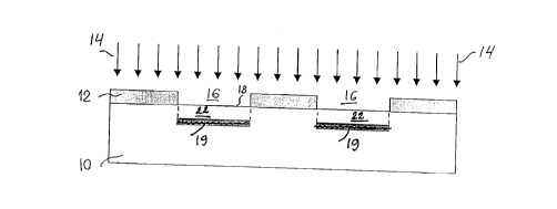
Fig. 1. The wafer 10 is patterned by selectively masking the
surface with a photoresist mask 12 (Fig. 1a). Then the
masked wafer is implanted with a suitable dose of helium
ions 14, which penetrate deeply into unmasked regions 16 of
the wafer 10, and majority of the ions come to the rest at a
projected range Rp, some distance below the surface 18 of
the wafer 10, the distance being the depth 20 of ion
penetration shown in Fig. 1b to 1d. The implanted wafer is
then rapidly thermally annealed at a rate and up to a
temperature causing selective explosive exfoliation, as will
be described in more detail below, causing separation of
pieces 22 of GaAs from the implanted regions, leaving a
CA 02246084 1998-08-28
7
complimentary structure with cavities 23 on the wafer (Fig.
1c). Thus the wafer 10 is patterned according to the details
of the mask 12 to the depth 20 determined by ion
implantation. Fig. 1d shows the wafer 10 after thermal
annealing and exfoliation of the implanted regions with the
mask 12 still on the wafer, the boundaries of the
complimentary patterned material remaining on the wafer
being designated by numeral 21. The mask is then removed as
shown in Fig. 1e.
The method will now be described in greater details
below. The GaAs wafer 10 is a conventional wafer having a
<100> oriented surface, having thickness of several hundred
micrometers and lateral dimensions of several centimeters.
Which may be partially processed to define microelectronic
or optoelectronic devices structures. Optionally, the wafer
is cleaned pre-treated in a conventional manner before
patterning, e.g. an oxygen plasma descum is used to remove
hydrocarbons, followed by a chemical etch to remove surface
oxides (e. g. 1:10 NH40H:H20 by volume, for GaAs). A vapor
treatment of hexamethyldisilazane is applied to promote
resist adhesion.
The wafer is then patterned by coating the wafer with
photoresist, i.e. Shiple 1827 photoresist, having thickness
of 3.5 micrometers using an SVGTM track and according to
program instructions. The photoresist is soft baked on the
SVG track, and exposed with Cannon wafer Stepper with an
appropriate reticle for approximately 0.86 seconds to
produce patterns in a range up to 100 micrometers
dimension, typical of those required for defining integrated
circuit devices and optoelectronics devices structures.
The wafer and reticle are oriented so as to achieve a
pre-determined orientation of the mask pattern to the
crystallographic directions of the wafer. The photoresist
CA 02246084 1998-08-28
g
is then developed conventionally, i.e. using SVG track and
MF319 developer, and hard baked at about 110C on the SVGTM
track. An oxygen descum is performed in a Tegal 901e
providing removal of about 300 angstroms of the photoresist,
after which the wafer exposed to a deep W light source to
cross link the mask pattern and to reduce pattern
distortion. Thus, the surface of the wafer 10 is
selectively masked with the resulting mask 12.
Implantation is performed by implanting a dose of
4x10¹⁶ of helium ions 14, having energy of 3 MeV and
penetrating into the wafer 10 to the depth 20 of about 4
micrometers. The depth to which exfoliation is required
determines the implantation energy. The required energy is
calculated using commercially available simulation software,
for example "TRIM", or from experimental measurement. A
typical energy is on the order of 1 MeV for a range of
depths of 1-2 microns, depending on the type of substrate.
In practice, the ion energy may range from tens of eV to
many MeV, depending on the application. The dose to which
the ions are implanted will depend to some extent on the
energy; typically a deeper implant requires a higher dose to
produce exfoliation. Typical implant doses are about 4x101s
ions/cm2 for a helium ion implantation and 1x101' ions/cmz
for a hydrogen ion implantation. The temperature of the
substrate during implantation is not critical if it is near
room temperature, so that typical beam heating effects on
the order of 50°C (producing a substrate temperature of less
than 100°C) does not significantly affect the outcome of the
process. For substrate temperatures significantly above room
temperature, the implanted ions may diffuse out of the
implanted region during the implantation step and therefore
exfoliation may not occur. Optionally, the implanted wafer
CA 02246084 1998-08-28
9
is stripped in the Gasonics for about 10 minutes at about
175°C, the step being repeated if necessary.
The annealing step is performed in a rapid thermal
annealer (RTA) where, after loading the wafer and purging
the chamber (e.g. with nitrogen gas), the temperature is
ramped rapidly (typically 2-10 seconds) to about 350°C.
Heating causes the implanted regions 22 to exfoliate from
the wafer. Since exfoliation typically occurs during the
temperature ramp-up, it is not necessary to hold the wafer
at the final temperature for any length of time. Then any
exfoliated pieces 22, which remain on the wafer, are blown
off with filtered nitrogen and collected. The photoresist
mask is removed from the wafer and exfoliated pieces by
chemical solvents or by plasma asking.
There is a minimum temperature required to achieve the
exfoliation process. The minimum temperature was determined
to be 300°C for GaAs or InP substrates, and 350°C was
preferred. In practice, the exfoliation process occurs
more completely when the temperature ramped as quickly as
possible to the minimum temperature. The exfoliation will
occur almost instantaneously across the entire wafer once a
critical temperature is reached. Heating beyond that point
appears to have no additional effect on the exfoliation.
There is a practical limit to how high an annealing
temperature. III-V semiconductor materials such as GaAs will
begin to decompose noticeably at high temperatures, e.g.
800°C; an overpressure P or As overpressure during
annealing may be used to suppress surface decomposition.
More significantly, in practice, diffusion of impurities
occurs well below decomposition, and may be detrimental to
structures or devices defined in the substrate. For example
diffusion of dopants may render active devices inoperable.
Therefore, the maximum temperature for the exfoliation
CA 02246084 1998-08-28
process is only a practical maximum dictated by other
devices or structures which are present on the wafer, and
when there is a need to minimize surface decomposition. It
may be possible to choose the order of fabrication for
particular devices so that the devices subject to a
restricted thermal budget are the exfoliation step.
The physics of ion implantation induced exfoliation has
been studied for many years, being initially focused on
exfoliation of thin films and blister formation in Nb under
He ion bombardment, see, e.g. articles by M. Kaminsky, IEEE
Traps. Nucl Sci. , NS-18, 208 (1971) and by S.K. Das and M.
Kaminsky, J. Appl. Phys., 44, 25 (1973). Recently the
research has been intensified in regard with a technology
known as "Smart-Cut" which relies on non-selective area
implantation of light ions into silicon and subsequent
annealing to induce fracture of a complete layer parallel to
the wafer surface, see, e.g. "Application of hydrogen ion
beams to Silicon on Insulator material technology" by
Michael Bruel in Nuclear Instruments and Methods in Physics
research B 108 (1996), p. 313-319. It was found that the
implanted ions lead to the formation of small platelets of a
size of a few nanometers between planes of the crystal. As
the dose increases, more of the platelets are formed, and
eventually they grow together to form voids or bubbles of
tens of nanometers in diameter. The implanted ions form a
pressurized gas within the bubbles. As the dose increases,
presence of the voids in the crystal causes stress which
eventually builds-up to the point where plastic deformation
occurs to relieve the stress, i.e. the formation of blisters
and flaking of the caps of the blisters. At the point that
this occurs, the blister is one large pressurized void. This
will occur at random points across an implanted region and
the blisters are typically quite large (1 millimeter). In
CA 02246084 1998-08-28
11
our experiments, the dose is only high enough to form small
pressurized voids where they have not yet grown together. We
believe that the annealing step causes the pressure of the
gas in these voids to increase to the point of plastic
deformation. The fact that the voids are still quite small
is important for producing sharply defined boundaries
between implanted and unimplanted regions, i.e. high quality
sidewall-facets.
A series of experiments has been performed, including
patterning of GaAs and InP substrates according the
description above with light ions of hydrogen and helium
having energies within a range of 800 keV to 3 MeV and doses
between 1x10¹⁶ ions/cm2 to 2x10¹⁶ ions/cm2. Masking was
accomplished by three methods: patterned photo resist on
GaAs, by Au patterns on the InP/InGaAsP/InP structures and
by thin Ni screens of various mesh dimensions (transmission
electron microscopy sample grids). The Ni grids, with
openings ranging between 50 and 250 microns on edge, were
held in close proximity to the sample surface during
implantation to provide square patterning. Typical results
of the experiments are illustrated by Figures 2 to 5. Fig.
2a shows a set of Nickel TEM grids 30, 32, 34 which had been
used in the experiments, and Fig. 2b shows an electronic
photograph of a top view of the single crystal InP patterned
according to the grid. A three minute anneal at 350C of a
sample of InP, which had been implanted with 450 keV energy
protons to a fluence of 1x101' cm-2, resulted in the
exfoliation of the material from the implanted areas. The
period array of the square recesses, 150 Nm on edge,
reproduces the image of the TEM grid that was used as an
implant mask. The newly exposed surface has formed at the
end of range (Rp ~ 3.6 Vim) of the implanted protons. The
sidewall-facets of the material remaining on the wafer are
CA 02246084 1998-08-28
12
shown in Fig. 3a. For this implantation the relative
orientation of the TEM grid and InP lattice was arbitrary.
Similar experiments have been performed for GaAs wafer and
the results are illustrated in Fig. 3b where the sidewall
formation is shown. Similar to designations of Fig. l,
numerals 18, 19 and 21 in Figures 2 and 3 correspondingly
represent the top of the wafer, bottoms and sidewall-facets
of the cavities made after exfoliation. As mentioned above,
the method described has a low sensitivity to final
annealing temperature. This result is illustrated by Fig. 4.
Fig. 4a and 4b correspond to annealing temperatures of 350°C
and 450°C respectively, the annealing ramp rate being the
same and equal to 100°C/sec. It is seen that the exfoliation
occurs in a similar manner, resulting in similar sidewall
formation and similar roughness of the bottom of the
cavities remained on the wafer. In figure 5, the importance
of the temperature ramp rate is demonstrated. At the lowest
ramp rate studied, 1°C/s, it appears that a single blister
has formed in each implanted region (fig. 5a). Although
these blisters have cracked open, most have lost a
relatively small fraction of the blister decke. At 4°C/s
ramp rate, exfoliation is occurring; however, it is still
very variable across the sample and where it appears it
largely incomplete (fig. 5b). An increase of the ramp rate
to 20°C/s, as shown in figure 5c, dramatically changes the
character of the exfoliation, which is now nearly total. By
100°C/s, figure 5d, the implanted regions are uniformly
exfoliated and the unimplanted regions remain intact,
without the imperfections observed at 20°C/s. Additionally,
at the higher ramp rates the exfoliated material is observed
to be primarily in the form of single blocks, released
intact from the implanted regions. These release
characteristics suggest that rapid temperature ramp produces
CA 02246084 1998-08-28
13
a more laterally uniform force on the overlayer, forcing it
away from the substrate and forming the walls along the
perimeter via cleavage. At lower ramp rates, the voids
likely combine to form a single blister which may then crack
open, releasing the trapped gas.
Exfoliation in a crystal containing a buried alloy
layer has also been observed (Fig. 6) . InP with a InGaAsP
layer 40 grown 2 Eun below the surface was masked with Au
stripes (not shown), each 2 ~.m thick, 8 ~m wide and several
millimeters in length. The stripes were deposited parallel
to the wafer flat, i.e. along a (100) symmetry direction of
the crystal. The mask was removed immediately after
implantation. Examination of the areas between the stripes
shows that there has been complete exfoliation, the result
of which is shown in Fig. 6. The sidewall-facets 21 are
observed to be relatively vertical, with imperfections near
the bottom of the wall 42, at the intersection with the
floor 19.
It was found that in the experiments where the mask had
straight edges oriented along [100] and [010] directions on
an <001> cut wafer exfoliation resulted in the formation of
extremely high quality sidewall-facets of pieces of the
exfoliated material and of the patterned material at natural
cleavage planes of the crystal. An SEM picture shown in Fig
7 illustrates typical results of the experiments where
vertical high quality sidewall-facets 21 of the patterned
structure remaining on the wafer are clearly seen. The
photoresist mask has been removed from the wafer before the
picture was taken.
The orientation of the sample with respect to the
incident ion beam and to crystallographic directions of the
wafer is an important parameter. When the ion beam is
parallel to a symmetry direction of the crystal, the ions
CA 02246084 1998-08-28
14
become channeled along that axis, for example along the
[100] axis, and they penetrate into the wafer slightly
deeper than would ions implanted along a non-symmetry
direction. To avoid ion channeling the implantation is
usually performed at a slight angle to the wafer surface
normal. In our experiments the angle was about 7° which
allows us to avoid channeling and to implant ions to the
calculated depth.
Instead of the method described above which includes
three basic step with the optional step of removing the mask
either before or after the annealing, alternative
embodiments of the method may include repetition of the
steps (a) to (b) a pre-determined number of times before
performing the step (c), i.e. masking and implanting may be
repeated several time before the annealing. It is possible
with an appropriate selection of a variety of masks
providing desired exfoliation of the material. The mask may
be removed after each implantation, or, alternatively, all
the masks may be removed together either before or after the
annealing step. In another embodiment it is also
contemplated that the steps (a) to (c) may be repeated as
many times as needed which means that the annealing step
takes place after each implantation. The mask may be removed
each time either immediately before or immediately after the
annealing step, or alternatively, all the masks may be
removed at the end of the process . It is necessary to keep
in mind that when several masks are formed on the surface of
the material simultaneously, they must have specific pattern
structures providing desired exfoliation of the material.
Alternatively, when using the same mask, multiple
implantations may be performed at different energies by
repeating the step (b) the required number of times which
allows deep patterning of the material, including patterning
CA 02246084 1998-08-28
through several layers of alloys. Different types of ions
may be used for different implantations, the mask being
removed either before or after the annealing step. Yet in
another embodiment of the invention which provides an
enhanced quality of the annealing, the step (c) of annealing
may be itself a multi-stage process, wherein multiple
annealing is performed, each subsequent annealing being
performed at a higher temperature than the previous one,
with the temperature of last stage annealing being performed
at the temperature required for exfoliation. In yet another
embodiment of the present invention the method may further
include a step of forming dashed trenches along pre-
determined boundaries/perimeter of the material to be
exfoliated to facilitate exfoliation of the material along
the boundaries, the step being performed before the step (c)
and in any sequence with the other steps. Preferably,
trenches are formed by etching, or, alternatively, by the
method of patterning of the present invention. Conveniently,
the depth of trenches is equal to or deeper than the depth
of patterning of the material.
Numerous modifications can be made to the, embodiments
described above. The wafer material 10 chosen to be GaAs or
InP in the first embodiment may be substituted by other
materials which are brittle enough to cause selective
exfoliation and to allow formation of pressurized voids
during implantation. They may include non-crystalline and
crystalline materials, including multi-layered semiconductor
structures. The mask 12 chosen to be made of photoresist in
the first embodiment may be formed of other materials, e.g.
metals (aluminum, gold, nickel), dielectrics (silicon
dioxide, silicon nitride) or combination thereof. The
requirements for the mask materials include 1) mask to be
thick enough to stop the implanted ions from reaching the
CA 02246084 1998-08-28
16
substrate through the mask, 2) to be robust enough to
withstand the implantation process without significant
deformations, and 3) straight edges of the mask should be
aligned with natural cleavage planes where the intention is
to produce high quality wall/facet. The mask can be removed
by chemical etching, plasma ashing or any other technique
which would not destroy the patterned structure. When the
plasma ashing is used, care must be taken not to heat the
wafer to the temperature of annealing as this may reduce or
prevent effectiveness of the exfoliation anneal. Ion
implantation which is done with H and He in the first
embodiment can be also done with other ions, e.g. ions of
inert gases or isotopes thereof. The requirement for the
type of ions is not to damage the surface of the wafer
substantially and to form pressurized voids within the
material which cause stress and further plastic deformation
of the material.
Although specific embodiments of the invention have
been described in detail, it will be apparent to one skilled
in the art that variations and modifications to the
embodiments may be made within the scope of the following
claims.