Note: Descriptions are shown in the official language in which they were submitted.
CA 0224613~ 1998-08-31
BACKGROUND OF THE INVENTION
i. FIELD OF THE INVENTION
The present invention relates to the field of signal
processing. More specifically this invention relates to gain
control in an amplifier circuit.
2. DESCRIPTION OF RELATED ART
Gain control is an important part of preventing distortion in
systems in which an amplifier must handle a wide range of inputs.
Improper gain control can result in clipping or distortion of the
amplifier output signal. One application in which amplifiers
process a wide range of inputs is in the processing of sound
signals. For example, an electrical signal generated from a human
voice may vary in signal strength dep~n~;ng on the person being
recorded, the language used and, the position of the speaker with
respect to a microphone. Typically, these voice signals are
received by commercially available microphones which output
signals varying from hundreds of microvolts to hundreds of
millivolts. A pre-amplifier may be used to amplify the signals
before input into a second stage amplifier. An automatic gain
control circuit adjusts the pre-amplifier increasing gain when
voice signals are weak and decreasing gain when voice signals are
strong to prevent overdriving the second stage amplifier.
42236.P042 1 PAT. APPL.
RWB/KMC/sjh
CA 0224613~ 1998-08-31
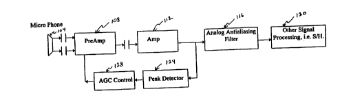
One arrangement for implementing a gain control circuit in an
amplifier system is shown in Figure 1. In Figure 1, a sound
signal is received by a microphone 104 which converts the sound
signal into an electrical signal. A preamplifier 108 amplifies
the electrical signal into a range appropriate for a more powerful
amplifier 112 typically a second stage amplifier. Processing
circuitry 116, 120, such as analog anti-aliasing filters 116
process the output of amplifier 112. A peak detector 124 also
receives the amplifier output signal. The peak detector detects a
local peak of the amplifier output signal 112 and generates a peak
indicator signal. An automatic gain control circuit (AGC) 128
receives the peak indicator signal and outputs a control signal
used to adjust the gain in an amplifier. The amplifier may be a
preamplifier 108 or the second stage amplifier 112.
In a prior art circuit implementation of a peak detector, an
AGC control circuit and a pre-amplifier, the peak detector circuit
inputs the output from amplifier 112 into an operational amplifier
within the peak detector 124. The peak detector 124 uses a
combination of operational amplifiers and transistors to generate
an output voltage correspon~;ng to the peak of the signal received
by the peak detector.
The output voltage, VAGC~ of the peak detector 124 is input
into AGC control circuit 128. Typically the AGC control circuit
uses a plurality of transistors to compare the voltage VAGC with a
reference voltage VDet to generate an AGC control signal. The AGC
control signal is related to the difference between VAGC and the
reference voltage VDet
~2236.P042 2 PAT. APPL.
RWB/KMC/sjh
CA 0224613~ 1998-08-31
A pre-amplifier 108 uses the AGC control signal to adjust the
gain of pre-amplifier 108. The gain of pre-amplifier 108
typically can be computed from the transconductance of transistors
within the preamplifier. The transconductance of these
preamplifier transistors multiplied by the resistance of a load
resistor typically determines the gain of the preamplifier. The
transconductance of the transistors in the preamplifier is a
function of the current flowing through the transistors. The
current flowing through the preamplifier is a function of the
output of the peak detector 124. Thus the gain of the pre-
amplifier depends on the output of the peak detector 124. AS the
output from the peak detector increases, the gain of the pre-
amplifier 108 decreases. Typical prior art gain control devices
are described in detail in U.S. Patent Application 5,241,494
issued to Blyth, et al. and U.S. Patent 4,890,259 issued to
Simko .
One problem with the previously described prior art technique
for implementing an AGC control is that the allowable dynamic
range of the microphones 104 into the preamplifier 108 is very
limited. When large over drive signals are applied to the input
of the pre-amplifier, (large over drive signals being defined as
on the order of tens of millivolts) severe distortion is created
and signal integrity is significantly degraded.
A second problem with stAn~Ard pre-amplifier gain control
designs is that the maximum signal gain is not very well
controlled. This is because the transconductance (GM) of
preamplifier transistors and the output load resistor which
42236.P042 3 PAT. APPL.
RWB/KMC/sjh
CA 0224613~ 1998-08-31
together determine the gain of the pre-amplifier do not track each
other. The resistance of the load resistor and the GM of pre-
amplifier transistors depend on independent process parameters,
thus substantial variations in production occurs. Either of these
components may have as much as a 30% variation due to variations
in process parameters.
Thus it is desirable to have a method and apparatus for
controlling the gain of the preamp stage which is able to handle
wide dynamic ranges while offering improved control of the gain.
422~6.P042 4 PAT. APPL.
R~nB/ ~ C/sjh
CA 0224613~ 1998-08-31
SUMMARY OF THE INVF~TION
A method and apparatus for adjusting the gain in an amplifier
or pre-amplifier is described. Variable resistors within the pre-
amplifier are electrically adjusted by a gain control circuit to
prevent over-driving of an amplifier receiving the output of the
pre-amplifier. In one embodiment of the invention, variable
resistors in the gain control circuit are adjusted after comparing
an input signal with a reference signal. Corresponding variable
resistors in the pre-amplifier track the variable resistors in the
control circuit preventing overloading of the amplifier.
42236.P042 5 PAT. APPL.
RWB/KMC/sjh
CA 0224613~ 1998-08-31
B~T~ DESCRIPTION OF ~ DRAWINGS
The advantages of the present invention will become more
readily apparent to those ordinarily skilled in the art after
reviewing the following detailed description and accompanying
drawings, wherein:
Figure 1 is a block diagram of a system utilizing an AGC
control circuit to control a preamplifier.
Figure 2 is one embodiment of a preamp of the current
invention.
Figure 3 is one embodiment of an AGC control circuit used to
control a pre-amp of Figure 2.
Figure 4 is one embodiment of a circuit to generate a
reference voltage used by the AGC control circuit of Figure 3.
Figure 5 is one embodiment of a circuit for performing full-
wave peak detection.
42236.P042 6 PAT. APPL.
RWB/KMC/sjh
CA 0224613~ 1998-08-31
DETATT~n DESCRIPTION OF THE INVENTION
In the following description and illustration, a number of
conventions will be used for convenience. For example, metal
oxide semiconductor (MOS) transistors are used in the circuit
embodiments described. A number of voltages will also be given
for illustrative purposes. It is to be understood that the
particular circuit layouts, the voltages used, and the use of MOS
transistors is done for illustrative purposes to facilitate
underst~n~; ng only and that one of ordinary skill in the art may
vary the design parameters and still remain within the scope of
the invention.
Figure 2 illustrates one example of a preamplifier 300 used
in the present invention. The preamp circuit 300 receives the
positive output 304 and the negative output 308 signals from the
microphone 104 as illustrated in Figure 1. Each microphone output
signal is applied to a correspon~; ng terminal of MOS variable
resistors 312 and 316 as illustrated in Figure 2. The opposite
tPrm; n~l of the variable resistors 312, 316 are coupled to the
inputs of a pre-amplifier operation amplifier (Pre-Amp Op-Amp)
320.
Variable resistor 312 and variable resistor 316 are
electrically adjustable. In one embo~im~nt variable resistor 312
and variable resistor 316 are MOS resistors. Each gate of each
variable resistors 312, 316 is coupled to a voltage source. The
voltage applied to the gate det~r~;nes the resistance of the
variable resistors. In one embodiment of the present invention,
42236.P042 7 PAT. APPL.
RWB/KMC/sjh
CA 0224613~ 1998-08-31
the control circuit 128, of Figure 1 generates a control signal
which is applied to the gates of variable resistors 312, 316 in
the pre-amplifier.
In the embodiment shown, resistors 324, 328 couple each
output of pre-amp op-amp 320 to a corresponding input of pre-amp
op-amp 320. The resistances of resistors 324, 328 are typically
kept constant. To facilitate fabrication of the pre-amp 300, the
constant resistors are typically MOS resistors with gates
connected to a constant voltage source VCl. Two other constant
resistors 332, 336 couple each input of pre-amp op-amp 320 to a
corresponding microphone input. In the embodiment shown,
microphone positive input 304 is coupled to a negative input of
pre-amp op-amp 320 via constant resistor 336 and negative
microphone input 308 is coupled to a positive input of pre-amp op-
amp 320 via constant resistor 332. In the illustratedimplementation constant resistors 332, 336 are also fabricated by
coupling the gates of MOS resistors to the same constant voltage
source, VCl.
The preamp circuit 300 produces a gain equal to: (the
resistance of resistor 324 divided by the resistance of resistor
332) times the positive microphone input plus (the resistance of
324 divided by the resistance of variable resistor 312) times the
negative microphone input. This may be expressed as:
Vout_ = (Ra/RC) x Vmicp + (Ra/Rb) X Vmicm-
If the Vmicp and Vmicm are symmetrical around a reference
voltage, the gain of the preamp may be expressed as the absolute
value of (Ra/Rc) - (Ra/Rb). The gain of the preamp is thus the
42236.P042 8 PAT. APPL.
RWB/KMC/sjh
CA 0224613~ 1998-08-31
difference of two ratios. The gain of this amplifier can be
controlled over a very wide range with the m~ximum gain well
defined.
The second term of the gain equation, Ra/Rb is a constant
because the gates of both resistors Ra 324 and Rb 332 are tied to
a constant voltage VCl. The value of the constant resistance is a
function of the MOS ~;m~n~ions including channel length and width.
In one embodiment, the ~;men~ions of the MOS resistors Ra and Rb
differ such that the second term of the gain equation (Ra/Rb) is
24.
The first term of the gain equation adds the ratio of the
resistance of constant resistor Ra 324 divided by variable
resistor Rc 312. Thus when variable resistor Rc 312 is a large
value, the overall gain is m~ximized. In the above mentioned
embodiment, the m~ximum gain occurs when Rc is set to a resistance
double Rb. This condition gives a ratio Ra/Rc of 12 and the gain
is 12-24 which is a gain of -12, for an absolute value of 12.
When variable resistor Rc 312 is set to a resistance equal to Rb,
the overall gain is m; n; m;zed. When the two ratios are almost
egual, the gain is near zero.
In one embodiment, the ~;m~n~ions (the length and the width
of the chAnnel in the MOS resistor) of constant resistor Rb 332 is
the same as the ~im~ncions of variable resistor Rc 312. Thus when
control signal voltage, VC2, is equal to the constant reference
voltage, VCl, the gain of the Amplifier 320 is zero because the
second term of the equation, Ra/Rb is equal to the first term
Ra/Rc. Thus reducing variable resistance Rc increases the term
42236.P042 9 PAT. APPL.
RWB/KMC/sjh
CA 0224613~ 1998-08-31
Ra/Rc of the gain equation, decreasing the overall gain of the
preamplifier. By varying a control signal VC2 which controls
variable resistors 312 and 316, the gain of the preamp circuit 330
can be adjusted.
Figure 3 illustrates an appropriate automatic gain control
circuit 400 (AGC control circuit) for generating the control
signal VC2. A comparator section 404 of the illustrated AGC
control circuit 400 compares the output from the peak detector 406
VAGC with a reference voltage 408 VDET. The comparison is done by
applying VAGC to a gate of a first comparison transistor 410 and
applying VDET 408 to a gate of a second comparison transistor 412.
The ratio of current driven by a current source 414 between the
two comparison transistors 410, 412 is determined by the relative
voltage of VAGC 406 with respect to VDET 408. When VAGC is less
than VDET most of the current flows through transistor 410 and
variable resistor R9 416 resulting in m;n;mAl current through
resistor 420. ~;n;mAl current through resistor 420 results in a
low voltage VSl at node 418 and switch Sl being open. AS VAGC
begins to rise with respect to comparison VDET, comparison
transistor 410 begins to turn off and more current flows through
comparison transistor 412 resulting in increased current flow
through resistor 420 and a rise in the voltage VSl 418. A rising
voltage VSl causes switches (Sl, S2) 426, 428 to change states.
The AGC control circuit 400 generates a control signal VC2 on
output 424 based on the comparator circuit 404 output VSl 418.
Comparator output VSl 418 is coupled to switches 426, 428. Each
switch 426, 428 is coupled to four resistors including two
42236.P042 10 PAT. APPL.
RWB/KMC/sjh
CA 0224613~ 1998-08-31
variable resistors and two constant resistors. In particular,
switch 426 is coupled to variable resistors 430, 432 and constant
- resistors 434, 436 while switch 428 is coupled to variable
resistors 438, 440 and constant resistors 442, 444.
In the illustrated embodiment, all resistors in the AGC
control circuit including the constant resistors 434, 436, 442,
444 and the variable resistors 430, 432, 438, 440 are MOS
resistors having the same ~;men~ions (channel width and length).
Thus constant resistors 434, 436, 442, 444 have the same constant
resistance because the voltage VCl 446 input to each gate of each
constant transistor 434, 436, 442, 444 is a constant. Variable
resistors 430, 432, 438, 440 vary together because the gates of
the MOS variable resistors 430, 432, 438, 440 are together
connected to a changing control signal VC2 voltage. Variable
resistors 430, 432 are coupled to a negative voltage reference 448
while variable resistors 438, 440 are coupled to a positive
voltage reference 450. Constant resistors 434, 436 are coupled to
a positive reference voltage 450 while constant resistors 442, 444
are coupled to negative voltage reference 448.
In the following description, voltage values will be used as
examples to facilitate the description and understAn~;ng of the
AGC control circuit 400 operation. However it is understood that
these values are exemplary values and other values may be used.
In an initial state of the AGC control circuit 400, the input
voltage from the peak detector VAGC is less than aE~ c,ximately 1.5
volts, while the reference voltage VDEr may be a~ oximately 1.8
volts. Analog ground is chosen to be around 1.5 volts. Negative
42236.PO42 11 PAT. APPL.
R ~ /KMC/Sjh
CA 02246l3~ l998-08-3l
voltage reference 448 and positive voltage reference 450 are
equidistant around the analog ground, thus if the analog ground is
1.5 volts, a typical negative voltage reference is 1 volt and a
suitable positive voltage reference 450 may be around 2 volts. A
typical Vc1 is around 2.5 volts. The initial control signal
output, VC2 initially may be around 2 volts.
During operation, control circuit Op amp 452 adjusts output
VC2 to eliminate voltage differences between input to control
circuit Op-Amp positive terminal input 453 and negative t~rm; n~l
input 454. In an initial turn-off stage, the input from the peak
detector 124 of Figure 1 is below the reference voltage VDET.
Thus the voltage VS1 at node 418 is at a low value and switches
426, 428 (S1, S2) are open preventing current flow through
resistors 426, 428. In order to equalize the voltages of the
positive input t~rmlnAl 453 and the negative input t~rm;nAl 454 of
control circuit op amp 452, the voltages at node 454 and 453 must
be kept equivalent. Keeping voltage at nodes 454, 453 equivalent
requires that the voltage at nodes 454 and 453 be maintAineA mid-
way between the negative voltage reference 448 and the positive
voltage reference 450 or that the resistances of the parallel
combination of variable resistors 430, 432 be kept equal to the
parallel combination of constant resistance 442, 444. Likewise,
the resistance of the parallel combination of variable resistors
438, 440 must be kept equal to the parallel combination of
constant resistors 434, 436. When switches 426 and 428 are open,
the resistance of resistor 434 (R3) must equal resistance of the
parallel combination of variable resistors 438, 440 (R5, R6). The
42236.Po42 12 PAT. APPL.
RWn3/KMC/sjh
CA 0224613S 1998-08-31
resistance of resistor 442 (R7) must also equal the resistance of
the parallel combination of resistors 430, 432 (Rl, R2). A feed
back loop feeding the output of the AGC control circuit to
variable resistors 430, 432, 438, 440. Thus the AGC control
circuit adjusts the output to satisfy the required resistor
equivalence of the AGC control circuit.
The control signal VC2 also controls the resistances of
variable resistors 312, 316 in preamp 300 and the variable
resistors 430, 432, 438, 440 in AGC control circuit 400. Thus all
variable resistors in the pre-amp 300 and the AGC control circuit
400 "track" each other by having the same resistance.
When VDET is greater than the voltage from the peak detector
VAGC , the switches Sl and S2 are open. To satisfy the requirement
that the parallel combination of variable resistor 430, 432 has
lS the same resistance as one constant resistor 442, each variable
resistor must have half the resistance of constant resistor 442.
When the variable resistance is equal to half the constant
resistance, the second term of the gain equation is 12.
Subtracting the second term (12) from the first constant term t24)
of the gain equation results in an overall gain of 12.
As an output of the amplifier slowly rises, the voltage from
the peak detector (VAGc) also rises and changes the relative
current flowing through transistor 410 and 412 in comparator 404.
The increasing current through transistor 412 raises voltage VSl
418 gradually closing the switches 426, 428. Closing switches
426, 428 reduces the effective resistance of resistor pairs 434,
436 and resistor pairs 442, 444. In order to maintain equivalent
42236 . P042 13 PAT . APPL .
RWB/KMC/sjh
CA 0224613~ 1998-08-31
voltages at nodes 454, 453, the resistance of resistors pairs 430,
432, and 438, 440 must also be reduced. Increasing the voltage
VC2 in the feedback loop reduces the resistance of variable
resistors 430, 432, 438, 440 maintA;n;ng equivalent voltages at
nodes 454, 458.
When VAGC is significantly above the reference voltage VDET,
the switches 426, 428 are completely closed. The similar
~;m~n~ions of variable resistors 430, 432, 438, 440, and of
constant resistors 434, 436, 442, 444 result in a VC2 equal to
VC1.
In the pre-amp circuit of Figure 2, the dimensions of
variable resistors 312, 316 are equal to the ~;m~nsions of
constant resistors 332, 336. Setting VC1 equal to VC2 changes the
resistances of the variable resistors 312, 316 (Rc, RF) to equal
the resistance of constant resistors 332, 336 (RB, RE)- Under
these conditions, the second term of the gain equation becomes the
same as the first term of the gain equation resulting in an
overall gain of 0. Thus as the input voltage increases, the gain
of the amplifier is reduced.
Figure 4 illustrates a circuit for generating a positive
reference voltages Vcl using VREF+ 504 and a negative voltage VREF_
508. The potential at VREF+ 504 and VREF_ 508 are an equal
distance from a common analog ground. The circuit of Figure 4
generates the constant voltage VC1 512 used in the circuits of
Figure 2 and Figure 3. In Figure 4, the output of a reference
op-amp 516 is coupled to a gate of a MOS resistor 520. An input
of the reference Op-Amp 516 and a t~rm;nAl for the MOS resistor
g2236.P042 14 PAT. APPL.
RWB/KMC/sjh
CA 0224613~ 1998-08-31
520 are coupled to a constant current source 524. A second input
of the Op-Amp 516 is maintained at a reference voltage, Vref. As
constant current source 524 pulls current through resistor 520,
Op-amp 516 maintains its output VCl to adjust the resistance of
MOS resistor 520 such that Vref_ is approximately equal to the
first input 508 of the Op-Amp 526.
Figure 5 illustrates a full wave peak detector 600 used as
the peak detector 124 of Figure 1. The full wave peak detector
600 includes two Op-Amps 604, 608. Op amp 604 receives a positive
signal from the second stage amplifier and a second op amp
receives the negative portion of the signal from the second stage
amplifier. Each op amp 604, 608 output is coupled to the gate of
a corresponding transistor 612, 616. The output voltage 624 is
common to each of the peak detector circuits with only one of them
active at any time. Since the peak of both the positive and
negative extremes are used, the resulting voltage 620 is smoother
and causes less signal distortion then a single peak detector.
The peak output of the peak detector at node 620 can be
determined by performing voltage division on the peak voltages
generated at the outputs of each op amp 604, 608 (at nodes 624)
between resistor 628 and resistor 632. The voltage divider steps
down the voltage to an appropriate value to produce voltage VAGC.
VAGC slowly decreases from the peak value by an RC time constant
determined by resistor 632 in parallel with capacitor 636.
While certain exemplary embodiments have been described and
shown in the accompanying drawings, it is to be understood that
such embodiments are merely illustrative of and not restrictive on
42236.P042 15 PAT. APPL.
RWB/KMC/sjh
CA 02246l3~ l998-08-3l
the broad invention, and that this invention not be limited to the
specific constructions and arrangements shown and described, since
various other modifications may occur to those ordinarily skilled
in the art.
42236.P042 16 PAT. APPL.
RWB/KMC/sjh