Note: Descriptions are shown in the official language in which they were submitted.
CA 02246303 1998-07-31
WO 97/29385 PCT/US97/O15S7
MICROSCOPIC IMAGING OF PROPERTIES OF ROOM-TEMPERATURE OBJECTS
FT_ET .D OF THE INVENTION
' The present invention relates to a device, which includes a cryogenic sensor
housed
within a vacuum space, for microscopy of physical properties of a room-
temperature object
located outside the vacuum space.
BACKGROUND OF THE INVENTION
In recent years, with the advent of microelectronics circuitry and related
advances in
electrical engineering, many industries have found a greater need to non-
invasively measure the
electrical and magnetic properties of materials and devices. The process of
magnetic imaging
at high spatial resolution and high sensitivity has been impractical, while
low sensitivity or low
IO spatial measurements have been unable to resolve crucial electrical
properties.
In the field of semiconductors/microelectronics testing, there is a need to
measure the
current flow and image the data relating to the operation of
semiconductor/microelectronic
devices and their related current paths.
With the advent of magnetic resonance imaging in the field of biology, many
new
discoveries have been made regarding biological and biochemical subjects.
Unfortunately, none
of the current technologies applied in this field provide a very sensitive
reading in the picotesla
range at low frequencies, or provide good spatial resolution at high
frequencies.
A number of techniques have been developed to image magnetic fields at length
scales
of a few ~cm or relatively smaller. These include decoration techniques,
magnetoresistive or
Hail probe sensors, magneto-optic thin films, magnetic force microscopy, and
electron beam
CA 02246303 2005-O1-07
-2-
interferometry. These techniques have provided limited success and are not
practical for high
resolution and .high sensitivity imaging of fields and flux lines.
Additionally, a number of susceptometers and magnetometers have been proposed
using
Superconducting Quantum Interference Devices, or SQUIDS. Though previous SQUID
systems have been developed to provide high magnetic field resolution, they
are impractical to
implement in a microscope imaging device. The prior art magnetic imaging
devices using
SQUIDS have had spatial resolution on the scale of a mm or larger which is to
crude for
microscopically resolving images. These devices may also require placing
samples in a
vacuum. 4f course, many samples such as liquids and biological specimens
cannot tolerate a
vacuum. Thus it is not practical to measure sources of biomagnetism which are
currently the
focus of much of the existing low-spatial-resolution SQUID imaging work.
U.S. Patent 5 , 4 91 , 411, entitled °Muthod and Apparatus for
Imaging Microscopic Spatial Variations in Small Currents and Magnetic Fields,
° by Wellstood
et al., discloses one such apparatus capable of providing all of the above
discussed
measurements with enhanced spatial resolution and magnetic field sensitivity.
however,
ahe device still requires placitag a sample within a dewar, which may result
in the unwanted
destruction of the sample when ii is exposed to the cryogenic liquid or
vacuum. Even if the
sample could tolerate the-vact3urtt environment or cryogenic environment, it
is time
consuming and cumbersome to introduce a sample into a vacuum space for
imaging. Another
shortcoming is the limited size of the samples that can be imaged.
CA 02246303 1998-07-31
WO 97/29385 PC'1'/US97/01557
-3-
STTMMARY OF THE INVENTION
Therefore, an object of the present invention is to conveniently measure the
physical
properties, such as the electrical and magnetic properties, of a sample.
Another object of the invention is to measure microscopic physical properties
of a
sample without destroying the sample.
Another object of the invention is to allow for magnetic and electrical
imaging of objects
which are bigger than objects now measured by conventional devices.
Another object of the invention is to allow the use of cryogenic sensors for
obtaining
microscopically spatially resolved images of physical objects of room
temperature samples.
Another object of the invention is to generate microscopic spatially resolved
images of
the magnetic and electrical properties samples at room temperature.
These and other objects of the invention are obtained by including a thin,
stiff,
transparent substrate or window within the outer wall of the vacuum space of a
dewar and a
cryogenic sensor within the vacuum space and spaced very close distances to
the window. This
construction allows for positioning a sample for measurement outside of the
vacuum space, at
room temperature or higher and for microscopy of physical properties of the
sample by
monitoring the output from the cryogenic sensor as it is scanned along the
surface of the
sample.
CA 02246303 1998-07-31
WO 97/29385 PCT/CTS97/01557
-4-
$ TF.F DESC TPTTON OF SEVE A WS OF TH T)RAWTN~~c
Fig. la is a schematic diagram of the device of invention.
Fig. lb is a fragmentary schematic view of features of the device of the
invention,
including a cryogenic sensor within the vacuum space of a dewar and a thin
transparent window
in the outer wall of the dewar.
Fig. 2 is a magnified plan view of the encircled portion of the device of Fig.
lb.
Fig. 3a and 3b are schematic views of a SQUID;
Figs. 4a through 4c show, in sequence, stages in the manufacture of a SQUID
and
sapphire point cold-forger, which is an example of the cryogenic measuring
device used in the
I0 present invention.
Fig. S shows a top view of the stage and mechanism for moving the stage upon
which
the sample is placed for measurement.
Fig. 6 is a schematic representation of a preferred embodiment of the
invention.
Fig. 7 is a diagram showing the scanning pattern used by the control program.
Dashed
lines show the paths of the SQUID (relative to the sample) during a scan.
Fig. 8 is a hierarchical format for data set.
Fig. 9a is a photomicroprint of the fine ink pattern around the portrait on a
$100 bill.
Fig. 9b shows the magnetic-field image with fields ranging from SOOnT (black)
to
500nT (white).
Fig. 10 is a vertical slice through the magnetic image shown in Fig. 9B
indicating a
spatial resolution of 50 ,urn.
Fig. 11 is a photograph of printed circuit board with arrows indicating
current flow
(100 ~,A) in wires.
CA 02246303 2005-06-27
-5-
Fig. 12 shows the static magnetic field image of current flow in printed
circuit board of
Fig. I1.
Fig. 13 shows a 49 KHz eddy-current image of a lap joint sample.
Fig. 14a shows a drive coil arrangement used for the eddy-current detection of
subsurface
cracks in conductors.
Fig. 14b is a side view of 14a.
Fig. 15 is a photograph of wire bent into a meander pattern carrying an
alternating current
at 400 MHZ.
Fig. 16 shows the radio frequency image of a 400 MHZ current flowing in the
wire
meander of Fig. 15.
DETAILED DESCRIPTION OF THE INVENTION
In a preferred embodiment of the invention, the apparatus of the invention is
composed of
a modified dewar, a cryogenic sensor, a stage, and a computer and its
associated software and
electronic connections to the stage to maneuver the stage.
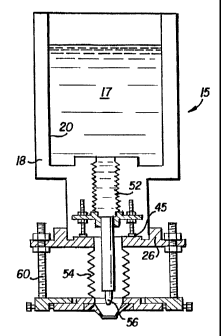
A major portion of the device of the invention shown in Figs. la and lb
includes
modified dewar assembly 15 having a vacuum space maintained at about 10-5 Torr
containing a
cryogenic sensor and a cryogenic space containing about twenty liters of a
cryogenic liquid.
In particular, dewar 15 shown in Fig. 1 is a modified commercial stainless
steel liquid
nitrogen dewar having a cryogen-containing portion 16 for receiving and
holding liquid
nitrogen 17, and a vacuum space 18 which thermally insulates the cryogen from
room
temperature. The modification consists of removing a portion of the
"superinsulation" 20 of
the commercial dewar and replacing the removed portion with an assembly 22
that includes
CA 02246303 2005-06-27
-6-
outer walls or housing 24, which defines the outer boundary of the vacuum
space of the dewar
and for maintaining a vacuum. Housing 24 is welded to the original dewar.
Housing 24
includes: an annular plate 26, having a circular opening 27 in its center, and
located radially
outwardly from central opening 27, on top of the annular plate, is circular
channel 49; a
transparent and thin substrate or window 28 located below and spaced apart
from annular plate
26; metallic bellows 29, connecting structures 30, plastic flange (ULTEM, a
nylon composition)
31 and glass slide window support 32 having an annular opening all of which
are structures
defining the distance between annular plate 26 and window 28 (see Fig. 2).
The modification to dewar 15 also includes bracing assembly 40. Bracing
assembly 40 is
composed of three footers 41 arranged in a triangular configuration relative
to each other,
grommet 43 having an annular exterior flange 44 and an annular interior flange
46. The bottom
ends of footers 41 are bolted on ring 45 seated in channel 49. Good mechanical
contact between
ring 45 and channel 49 is achieved by tying nylon bristles 42 around ring 45.
This construction
also ensures a weak thermal contact between the bracing assembly 40 generally
maintained at
77°K and the room temperature plate 26 and window 28. Bracing disk or
plate 47 located
approximately one inch from plate 26 and parallel thereto has three holes 48
for receiving
complementarily threaded footers held in place by nuts. Plate 47 is connected
to the grommet by
bolts to exterior flange 44.
The annular plate 26 as shown in Fig. 1 a is also connected via threaded rods
60 to
horizontal adjustment annular disk 62 with adjustment screws 63 positioned as
shown. Vertical
adjustment nuts 64 on rods 60 are positioned on each side of the annular plate
and allow fine
movement of window 28 with respect to SQUID 72.
CA 02246303 2005-06-27
_7_
The final modification to dewar 15 is cryogen delivery system SO that includes
stainless
steel bellows 52, copper or brass tube 54, and thermally conducting substrate
56 preferably a
sapphire rod. Stainless steel bellows 52 is sealed to and is in open
communication, at a first end,
with the cryogen-containing portion 16 of dewar 1 S. The second end of
stainless steel bellows
52 is located in the vacuum space 18 and is in open communication with the
annular inner space
of the grommet 43. This second end of bellows 52 is seated on the top of
interior flange 46 of
the grommet. The purpose of this assembly is to cool the cryogenic sensor 70
SQU>D chip 72
See Fig. 4c to operating temperature while simultaneously holding them rigid
with respect to the
dewar and minimizing the effects of thermal contraction in dewar walls 16.
The first end of copper tube 54 is received in the bottom inner annular space
of the
grommet 43 and is seated and soldered on the bottom of interior flange 46 of
the grommet and is
in open communication with the annular space of the grommet. Tube 54 extends
through
vacuum space 18, and through opening 27 in annular plate 26. Located in the
second end of tube
54 and fastened thereto with epoxy is one end of thermally conducting
substrate 56 which is
sapphire and rod-shaped. The second end of the rod-shaped substrate is
fabricated with a blunt
end point, to which is fastened chip 72 positioned within an adjustable
distance and preferably
within a few microns of window 28 the adjustment being provided by adjustment
rod 60 and nuts
64. Specifically, the distance between chip 72 and window 28 may be as great
as 2-3 mm or
there may be no distance between them when they are touching. This
construction allows for
maintenance of sensor temperature at 77°K while allowing for minute
separations between the
sensor and a room-temperature sample.
It is pointed out that at room temperature the stainless steel bellows 52
exerts a force on
bracing assembly 40, holding it in good mechanical contact with annular ring
26. When the
CA 02246303 2005-06-27
_g_
cryogenic liquid is introduced into the dewar so that the liquid passes
through the stainless steel
bellows 52 and the copper tube 54, dewar 16 will contract but the position of
the point will be
unchanged because bellows 52 will stretch. Tube 54 will also contract, but
this movement is
countered by the contraction of footers 41, which are in heat exchange contact
with the cryogenic
liquid through connection to plate 47 and copper grommet 43.
Of course, by constructing the footers of zinc and other metal parts of
copper, brass and
stainless steel as described or of other metals, and noting the physical
expansion and contraction
properties of such metals, thermal expansion and contraction of the parts can
be anticipated such
that the sapphire rod and cryogenic sensor do not move at all or move very
little upon cooling or
warming of the dewar. Correction of any such movement of the sapphire rod in
the vertical
direction can be accomplished by hand, by adjusting vertical adjustment nuts
64. Lower bellows
29 allows for such movement.
As indicated above, an improvement of the invention is the microscopic imaging
of a room
temperature object or sample located outside of the dewar with the ability to
bring a cryogenic
sensor within microns of the sample. To this end, the apparatus of the
invention includes a
scanning sample stage 90 see Fig. S that is located outside the dewar which is
a considerable
simplification as compared to stages used in previous scanning SQUID
microscopes. Such
stages required precision engineering for thermal contract and careful design
to overcome the
lack of lubrication in cryogenic temperatures. Notwithstanding the temperature
advantage, the
requirements of the scanning stage used in the present invention are similar,
for instance, to the
stage disclosed in U.S. Serial No. 08/061,102. In particular, the mechanism
should have a 1
pm positioning accuracy; it should ideally be non-magnetic and non-metallic,
and preferably the
stage is motorized. In addition to the capability of moving in the x -y
directions, stage 90
CA 02246303 1998-07-31
WO 97/29385 PCT/US97/O1SS7
-9-
should also have capability of moving in the vertical direction in order to
raise or lower the
sample to the window of the invention and allow for easy insertion of samples.
A vertical
translation stage similar to the height adjustment mechanism used in a
standard optical
microscope can be used. The vertical translation stage can be mounted above or
below the x y
scanning stage allowing distances of between 2 inches to ~.m lengths between a
sample 91 (see
Fig. 2) on the stage and window 28. In fact, the sample can be touching the
window. The
vertical translation part of stage 90 used in the present invention is
commercially available and
was purchased from Edmund Scientific Co. as part no. J3608. Although this is a
metallic
stage, a one-inch thick plexiglass stand-off or spacer is placed between a
sample and stage 90
to prevent undesirable magnetic interference from the metal of the stage to
the cryogenic
sensor. Also, limited success in removing residual magnetization was achieved
by degaussing
the steel components in stage 90 using a bulk magnetic tape eraser.
The stage 90 and stepper motors 92 for driving the x and y axes of stage 90
are shown
in Fig. 5.
To automate the scanning process, motors 92 are used to drive the scanning x y
stage.
Unfortunately, undesirable magnetic fields produced by the motors can easily
couple into the
SQUID because there is virtually no magnetic shielding between the SQUID and
motors 92.
Therefore, it is important to mount the motors as far as possible from the
SQUID (about 50 cm)
and to envelope them in eddy-current magnetic shields such as 1.5 mm-thick
aluminum box 94
ZO as shown in phantom in Fig. 5, which provides magnetic shielding above
about 1 kHz.
Motors 92 are mechanically coupled to micrometers 95 and single shafts 96 (x-
axis) and a
spline 97 coupled to and a right-angle coupler 98 (y-axis) through a 10:1
reduction right angle
gear box 99. This design allows one to easily change the separation between
motors and stage
CA 02246303 1998-07-31
WO 97/29385 PCTIUS97/O1SS7
-10-
by simply extending shafts 96. Although magnetically noisy, stepper motors and
microstepping
drives are used because they provide excellent positioning accuracy.
The CPU with controlling software and peripherals for operating the motor, is
shown
in the block diagram of Fig. 6.
In greater detail, thermally conducting substrate 56, in a preferred
embodiment, is a
sapphire rod, one-inch long with a 0.25 inch diameter. Sapphire has a large
thermal
conductivity at low temperatures (at 77 °K, about 10 W crri'deg 1).
Substrate 56 supports the
cryogenic sensor 70 which, in a preferred embodiment is a SQUID chip 72 (see
Figs. 3a and
3b).
SQUID chip 72 consists of a single 200 mm-thick layer of YBazCu30., as known
in the
art, is deposited on a 500 ~cm thick, l0mm by l0mm SrTiO3 24° bicrystal
substrate using
pulsed layer deposition. See, for instance, R. Gross et al., "Low Noise
YBa~Cu30~_ Grain
Boundary Junction do SQUID," Appl. Phys. Lett. Vol 57, p. 727 (1990), herein
incorporated
by reference. The SQUID sensor 70, as shown in Fig. 3a, has a square washer
shape with an
inner hole size of about 20 ~cm and an outer size of 60 ~cm. This geometry
gives a measured
effective magnetic pick up area of approximately 1.33 x 1Q9m2. Gold contacts
77 are deposited
onto the chip as shown.
Since the SQUID is small it is difficult to handle. The small chip requires a
special
mounting procedure which is shown in Figs. 4a through 4c. Once a working SQUID
is
obtained on a SrTi03 chip, the chip side of the sensor is epoxied to an end of
the one-inch long,
0.25 inch diameter sapphire rod using STYCAST 2$50 FT epoxy, creating the
structure shown
in Fig. 4a. To ensure an adequate bond the mating surfaces of these structures
were also
etched. The SrTi03 epoxy and sapphire are then ground away using a diamond-
grit poiishing
CA 02246303 2005-06-27
-11-
wheel leaving a 800 ,um-diameter tip at the end (see Fig. 4b). Additional
epoxy may be used
to coat exposed edges. The tip consists of the disk of SrTi03 containing at
least one SQUID
and gold contacts. To make the electrical contact to the surface of this chip,
three silver
contacts 78 about 200 nm thick are deposited over the edges of the chip and
down the side of
the sapphire rod (see Fig. 4c).
As is known in the art, SQUIDS are usually operated in a negative feedback
loop or
flux-locked loop.
To couple magnetic flux into the SQUID for maintaining a flux-locked loop, or
for
applying the read-out flux required for other imaging schemes, a simple three-
turn coil 80 was
wrapped around the sapphire rod as shown in Fig. 2. A mutual inductance of
approximately
0.24 pH between the SQUID loop and the coil was measured. It is determined
that mutual
inductance can be increased by fabricating an electronics squid output
feedblock coil 80
directly on the SQUID chip using photolithographic printing techniques known
in the art.
A field coil 82, for applying a magnetic field to a sample, has a diameter
perpendicular
to the longitudinal axis of the sapphire rod and is shown in Figs. la and lb,
and may be wired
to electronic measuring or controlling equipment as schematically shown in
Fig. 6.
As discussed above, the design of window 28 Fig. 2 separates the SQUID chip 72
which
is in vacuum space 18, from a sample 91 which is in air located outside of
dewar 15. In order to
obtain images of physical properties with spatial resolutions as fine as SO
~.m, the separation of
SQUID and sample should not be great and should be within 50 pm. To achieve a
better spatial
resolution, the SQUID must be smaller and closer to the sample. In order to
accomplish this
result, the window 28 must be thin and at the same time sufficiently broad to
accommodate
the SQUID chip, which must be positioned within a few ~Cm of the window. The
minimum
CA 02246303 2005-06-27
-12-
width of the window depends on the width of the blunt end of the rod 56. In
addition, window
28 should be stiff so as not to flex substantially under an atmosphere of
pressure. That is, the
window will flex less than its thickness under one atmosphere; flexing of the
window will
necessarily increase separation between the SQUID and a flat sample. The
window must also
maintain a vacuum and it must be chemically inert, non-conducting and non-
magnetic so that
it does not interfere with the SQUID or react with a sample. Additionally,
because it is very
likely that the SQUID sample may accidentally contact the window, the window
must be
durable and must tolerate repeated contact with the sample. Finally, it has
been noted that the
window should preferably be transparent to the human eye (or to infrared or UV
radiation
which can be viewed with appropriate imaging systems) to help align the
window, SQUID,
and sample prior to a scan of the sample.
It has been found that transparent material having a Young's modulus of about
70 GPa
to 670 GPa should be used. Preferably, this is a single-crystal sapphire
(A1203) which is
transparent and has a Young's modulus of about 50 x 106 psi.
Some materials which are suitable for windows include plastic, diamond,
metallized
films, MgO, SiN, LaAl03 and combinations thereof, as well as other materials.
In addition, as
discussed above, such materials should also be transparent. Window 28 is built
by creating a
window frame that includes drilling a conical hole in a 1.25 mm thick glass
microscope slide
32 using a silicone-carbide tool. The diameter of this hole is lmm on the
sample side and
3mm in diameter on the SQUID side (see Fig. 2). The window frame may be made
from any
suitably stiff material including epoxy, glass, sapphire, diamond, etc.
Thereafter, a 25 p.m-thick, 1 cm x 1 cm single crystal of sapphire 30 is
epoxied to the
sample side of the glass slide 32 to form the 1 mm diameter, 25 pm-thick
window 28 according
CA 02246303 2005-06-27
-13-
to the following procedure. Having obtained this small window, it is waxed and
adhered to a
small glass holder. The window is then epoxied to the window frame 32 while it
is still waxed
to the holder. Once the epoxy hardens, the glass holder is removed by boiling
the whole
assembly in water to melt the wax. The total time in water should be kept to a
minimum,
because the water tends to temporarily soften the epoxy. The remaining side of
the glass slide
is epoxied to plastic flange 31 (see Fig. 2) which is then mounted to the
dewar assembly
through connecting structure 30 as shown in Fig. lb.
When setting up the microscope for imaging, the alignment of the window with
respect
to the SQUID is critical. Alignment is accomplished by using an optical
microscope and a
mirror to look directly through the thin sapphire window at the SQUID. The
roughest approach
is to simply move the window by adjusting nuts 64 or screws 63 until it
touches the SQUID.
With moderate relative humidity, it is possible to observe water condensing on
the window
when the SQUID is contacting the window. This is helpful for leveling the
window with
respect to the SQUID chip since the fog on the window indicates the location
of contact
between the SQUID and window.
It is also possible to detect thermal contact between the SQUID and the window
by
simply observing the SQUID voltage on an oscilloscope when oscillating flux is
being applied
to the SQUID. The degradation of the SQUID performance is quite sudden and
significant
when SQUID contact is made. Once the window is leveled with respect to the
SQUID, the
sample and scanning stage must be leveled with respect to the window. Leveling
of the sample
with respect to the plane of motion of the stage ensures that the separation
between the sample
and SQUID does not change during a scan. Leveling of the stage with respect to
the window
CA 02246303 1998-07-31
WO 97/29385 PCTIUS97/01557
-14-
is necessary for achieving a small separation because of the relatively broad
(1 cm) glass slide
on which the sapphire window is mounted (see Fig. 2).
To obtain an image of the physical properties of a sample, individual raster
scan lines
are acquired by scanning the sample past the SQUID in the x direction while
simultaneously
recording the x coordinate and the relevant voltages (static field signal, rf
field signal, eddy-
current signal, etc.) from the SQUID read-out electronics. This is repeated
for the sequence
of y values to construct the whole image.
The position of the stage is determined exclusively from the stepper-motor
position.
The control program of the computer 100 can read the stepper-motor position
directly from the
IO motor controller board which is mounted in computer 100. However, for
proper
synchronization of the x coordinate with the SQUID signal during a scan in the
x direction, it
is necessary to provide the data acquisition system with a voltage signal
which is proportional
to the instantaneous x position of the stage. This is accomplished using an
external counter
circuit which simply keeps track of the number of motor steps and adds this
to, or subtracts this
IS from, a position counter depending on the motor direction. The output from
this counter is
converted to a voltage level by using an integrated digital-to-analog
converter. Hence, the
counter simply functions as a position-to-voltage taransducer.
Both the SQUID output and the position of the stage are read using an analog-
to-digital
converter and recorded using a personal computer. The personal computer also
controls a
20 scanning operation which generates the grid of position coordinates. Once a
data set has been
acquired using a control program, it is converted into an image. In its raw
form, the image
data consists of a set of "N" line scans (y-values) with the ith line
containing a set of 1V~ data
points each having an x coordinate and one or more associated voltage values.
To provide an
y. i! ~:..1 i:~,~ ~ ,~:.g ~ ~.....~~ ,. R" .~_~
CA 02246303 1998-07-31
WO 97/29385 PCT/US97/01557
-15-
image, this data is first spatially regularized, i. e. , linearly interpolated
onto a rectangular
spaced grid. Then an image rendering program is used to assign a color, or a
level of gray to
each grid point.
The sample stage 90 can be moved by manually operating drive screws and a very
simple data acquisition program can be used to record the position of the
sample stage using
potentiometers attached to the x and y drive screws on the microscope while
simultaneously
recording the SQUID output. A second program to convert the stream of
positions and values
into a set of values on a rectangular grid can be used and finally each value
in the grid can be
assigned a color and an image can be displayed.
This procedure, especially scanning the sample manually, is quite time
consuming and
monotonous. Accordingly, a control program has been written and is used to
operate the stage,
record the SQUID output and then display an image.
In essence two stepper motors are operated using a controller board which is
physically
mounted in computer 100 along with a multifunction input-output (IO) board
which is primarily
used as an analog-to-digital converter (ADC) for reading the output from the
SQUID
electronics. Hence, both motion control and data acquisition are accomplished
using a single
personal computer.
Since the SQUID is basically a point-like probe, it must be scanned in a
raster pattern
to form an image. The raster pattern consists of a series of lines in the x
direction at different
values of y, stacked together to form an image.
To take an image with the microscope, the computer first positions the sensor
70 to the
"home" position x = .xs,a,~ - xo~ershoot~ Y = Y~ ~ where xS~ corresponds to
the left edge of the image
area, yl is y coordinate of the first scan-line and ~"ers,~ot is the
hysteresis length in the x scanner.
CA 02246303 1998-07-31
WO 97/29385 PCT/US97/01557
-16-
(see Fig. 7). It is necessary to overshoot the left edge of the image area by
~~e~shoo~ prior to
scanning each line to eliminate the backlash in the scanning mechanism. Next,
the x position
of the SQUID is increased at constant velocity (to the right) until x = .~~a«
at which point the
computer begins recording the x position and the SQUID signal Vo"I. If needed,
additional
channels of data, up to the limits of the IO-board, can be acquired at the
same time. The data
is continuously sampled until x = xe"~ at which point the data acquisition for
this scan-line ends
and the single scan-line is written to the data file. At this point the x
position of the SQUID is
"rewound" to x = xs~aa - xovershoot, and the y- position advanced to y y2 in
preparation for
acquiring the second scan-Iine. This procedure is repeated until all N scan-
Iines are acquired
and written to disk.
Once all N scan-lines have been written to the data file, they must be
converted into an
image. To accomplish this, the individual scan-Iines must be spatially
projected onto a
rectangular grid. While the raster lines at yl, y2 . . ., y" are evenly spaced
in the y direction,
the data points in the x direction are not regularly spaced with respect to
each other. That is,
while the data points in any given scan-line may be uniformly spaced, they may
be shifted with
respect to an adjacent scan-line. Hence the program must line up the x values
in all the scan-
lines by defining an evenly spaced grid in the x direction and then computing
Vout at each of
these points by linearly interpolating the data from the raw scans.
Once this is done, all that is left to do is to convert the resulting uniform
grid of values
into an image by assigning colors or shades of gray to each value in the grid.
Various
commercially available computer programs can be used to do this. One such
program is called
"Transform," produced by Spyglass, Inc. in Champaign, Illinois.
CA 02246303 1998-07-31
WO 97/29385 PCT/IJS97/01557
-17-
An important capability of this software is the ability to select an arbitrary
"scan"
variable and "raster" variable. While in the description of the scanning
procedure above, x was
chosen as the "scan" variable and y as the "raster" variable, with this more
generalized
approach to selecting the independent variables, it is equally acceptable to
scan the y coordinate
and treat x as the raster variable. Furthermore, other parameters for the scan
coordinate could
be chosen. For instance, the computer can also control the voltage output from
a digital-to-
analog converter in the IO-board which can subsequently be used to set the
frequency of an rf
source used for, say, driving the sample. Hence, it is sufficient to produce
an image containing
frequency versus x by choosing the frequency of the rf source as the "scan"
variable and the
position of the x motor as the raster variable. Obviously many other
combinations are possible
as well.
Since the "scan" and "raster" variables can be chosen independently, it is
naturally
possible to use the same program with different microscopes and sensors. This
is done by
simply choosing the scan and raster variables for the appropriate microscope.
Often it is useful to program a series of image acquisitions to occur under
program
control. For instance, suppose one would like to take an image, change a
parameter, take
another image, change a parameter again and continue, thus producing a
sequence of images
suitable for a movie. To address this, the program has a variety of
programming features which
allow the acquisition of images without operator intervention. This is
accomplished by
organizing the multiple images into a single "set" which consists of an
arbitrary number of
"scenes." Each "scene" can contain an arbitrary number of "frames." And each
frame
represents a single image, composed of multiple scan-lines of data points (see
Fig. 8). The
parameters for a particular "scene" determine which variable is used for the
"raster" variable
CA 02246303 1998-07-31
WO 97/29385 PCT/LTS97/O1S57
-18-
and which for the "scan" variable. Also the 'scene" determines the values for
~.t~".~, xend~ ym
Yz, ..., yN, scan speeds, data sampling rates, and most other imaging
parameters. So, if one
wants to acquire a number of virtually identical images with only, say, a
single parameter
change between images, a single "scene" will be used with multiple frames. The
"set" is
simply a sequential ordering of any number of different "scenes" to be
acquired. With this
structure, it is possible to program virtually any combination.
An important part of data acquisition is recording the operating parameters of
the system
when the data is taken. In order to assure reproducibility, all relevant
parameters must be
saved. With this program, this is done by using a "document" type interface
for data sets.
After a data set is acquired it is held in a temporary buffer area. The "set"
can then be save
along with all the relevant parameters in the data acquisition program which
were in effect
when the data was acquired. At a later time, this data set can be opened and
read back into the
program thus returning all the parameters in the program including the buffer
file to the state
it was in when the data was originally taken. Hence, each of these saved data
sets represents
IS a snap-shot of the state of the program after imaging and hence contains a
complete record of
the imaging parameters. This saves a great deal of time usually spent writing
down parameter
values in a notebook.
To demonstrate the ability of the microscope to image static magnetic fields,
a
ferromagnetic sample and a sample carrying a do current were imaged. In each
case the
microscope is operated in a flux-locked loop.
Figure 9(a) shows a photographic image of the fine printing (rnicroprint)
around
Benjamin Franklin's portrait on a $100 U.S. Federal Reserve Note. Figure 9(b)
shows the
corresponding static magnetic field image of the same region. The ink in this
sample is
CA 02246303 1998-07-31
WO 97/29385 PCT/LIS97/01557
-19-
ferromagnetic and hence produces a substantial magnetic signal. To achieve the
best spatial
resolution, the sample was scanned in direct contact with the sapphire window.
This is possible
because of the flatness of the sample and the hardness of the window material.
The magnetic
fields in the image range from -500 nT (black) to 500 nT (white). These field
variations are
about 1000 times larger than the noise threshold of the image and so this
sample does not
necessarily demonstrate the field sensitivity of the instrument. However, the
small feature size
in the sample does provide a good test of the spatial resolution.
The spatial resolution of the instrument can be deduced from Fig. 10 which
shows a
vertical slice (from bottom to top) through the magnetic image in Fig. 9(b)
along the line
IO indicated by the triangle. By measuring the full width at half maximum of
the sharpest peak
in this and similar slices, a spatial resolution of about 50 ~cm is deduced.
The data indicates that
the separation between the SQUID and the surface of the sample should be less
than SO ~cm.
This is about a factor of 30 times smaller than any other previously published
SQUID-based
system which can image room-temperature samples in air.
In an environment where the microscope would be used for nondestructive
testing
applications, the quasistatic fields are more likely to be produced by flowing
currents.
Figure 1 i is a photograph of a small portion of a printed circuit board
showing a number of
copper interconnects and solder points. A current of 100 ,uA is flowing in the
wires as
indicated by the arrows.
Figure 12 is a magnetic image of this sample obtained by scanning at a
separation of
about 200 ~m between the window and the surface of the circuit board. While
the spatial
features in this image are not difficult to resolve, the fields produced by
the currents, which
range over about 80 nT, are considerably smaller than before. Hence, it was
necessary to first
CA 02246303 1998-07-31
WO 97!29385 PCT/US97l01557
-20-
obtain a background image without the sample, then subtract this from the raw
magnetic image
of the circuit board.
The image clearly indicates which conductors are carrying a current and which
are not.
Also, by application of the right-hand rule, it is possible to determine the
direction of current
flow. Furthermore, magnitudes of the currents can also be extracted in
principle by modeling
the field produced by a current I in one of the interconnects. Because the
data used to generate
the image is quantitative, a fitting algorithm could be utilized to find 1.
Even in the case where
the density of interconnects causes significant overlap of the fields in the
image, more advanced
deconvolution algorithms can be used to extract the directions and magnitudes
of the currents.
Note that circuit boards like the one shown inevitably contain magnetic
contamination
in the form of small particles of steel, resulting from handling or machining.
One such particle
110 is seen in the lower right corner of Fig. 12 where it produces a
characteristic dipole
signature. However, even if a contaminant 110 does not have a strong magnetic
signature, it
may also be detectable when it is located in a conducting pathway where it
could degrade circuit
performance. For example, note the distinctive effect of the current flowing
across the solder
point 112 near the bottom of Fig. 12. The perturbation of the current by the
hole alters the
field as is easily seen in the image. While the hole is rather larger in this
case, the clarity of
the image suggests that much smaller nonuniformities in current flow could be
detected. This
technique could ultimately be use to detect small voids or particulate
contamination in critical
conducting pathways, possibly beneath the surface, which would otherwise not
be apparent until
after the circuit failed.
CA 02246303 2005-06-27
-21-
In some cases, it is not possible or practical to directly inject currents
into a sample for
imaging. However, by applying an alternating magnetic field to the sample,
alternating eddy
currents can be induced in the sample for probing defects.
To further illustrate the capabilities of the microscope, eddy-current images
of a variety
of metallic samples, including an aluminum "lap joint" assembly as used in
aircraft fuselage
construction were tested. A lap joint is where two sheets of aluminum skin are
joined together
and riveted to a support strut. The detection of defects in lap-joints is the
goal of some of the
existing eddy-current NDE efforts.
A '/4-scale model of an aluminum (resistivity p ~.6 ~S2 cm at 77 K) lap joint
was
constructed. In the scale model, an upper and lower sheet of 0.2 mm-thick
aluminum are
jointed to a 0.8 mm-thick support strut by means of 1.6 mm-diameter rivets
with 2.5 mm-
diameter heads. The rivet heads are made flush with the sample surface as is
done in real
aircraft construction. A crack 114 which extends to a radius of about 3 mm
from the center
rivet was placed in the bottom layer of the skin so that it is not visible
from either the top or
bottom of the assembled sample. The crack was formed by shearing the metal and
then
flattening it again before riveting the sample together; this leaves a very
tight crack with no
gap.
Figure 13 shows a 49 kHz eddy-current image of this sample. To obtain the best
results,
a linear drive wire oriented in the plane of the sample to induce eddy
currents, as shown in Figs.
14a and 14b was used. This induces eddy currents which are strongly perturbed
by the
geometry of the crack. In addition to the five rivets, the buried crack which
extends diagonally
from the center rivet is clearly resolved in this image. Other structure is
also visible in this
CA 02246303 1998-07-31
WO 97/29385 PCT/LTS97/01557
- 22 -
image. For example, the image indicates the presence of the thicker support
strut in the region
beneath the rivets.
Since many electrical circuits operate at high frequencies, another
potentially important
imaging technique involves imaging the rf fields produced by rf currents
flowing in a sample.
For example, silicon-based high-frequency circuits are not designed to
function at 77K. The
ability to examine room-temperature samples makes it possible to apply the rf
imaging
capabilities of a scanning SQUID microscope to this class of samples.
To test the microscope's rf field imaging capabilities on a room-temperature
sample,
the rf fields in the vicinity of the wire-meander sample shown in Fig. 15 were
imaged. A 400
MHZ rf current is driven in the wire using an rf voltage source. Figure 16
shows the rf image
of the 400 MHZ fields produced over the surface of this sample. The brightest
regions
correspond to an rf feld magnitude of about 200 nT. The darkest regions,
including the lines
corresponding to locations of the wire, are where the z component of the field
is zero. This
image emphasizes the point that, when configured for imaging rf fields, the
microscope is only
IS sensitive to field magnitude and not field amplitude.
In previous work, it was found that the maximum frequency at which this
technitque
functioned properly was about 150 MHZ. Beyond this, cavity mode resonances in
the SQUID
substrate produced artifacts in the images and effectively degraded the
spatial resolution.
Clearly, Fig. 16 shows that the bandwidth of the room-temperature microscope
is higher for
this type of imaging. The reason for this improvement is that the substrate
size is a factor of
4 smaller in the room-temperature system. By using a smaller SQUID substrate,
the frequency
at which the lowest cavity mode will oscillate is increased proportionately,
along with the
frequency at which the image deteriorates.
CA 02246303 1998-07-31
WO 97/29385 PCT/LTS97/01557
- 23 -
While the above images were made using a SQUID, many other types of cryogenic
sensors could be used. The advantage of using other types of cryogenic sensors
is that, when
used in the apparatus, they will allow the sensitive microscopic imaging of
other physical
properties which the SQUID is not sensitive to.
Such cryogenic sensors include: bolometers for imaging microwave, optical, UV,
and
infrared radiation; multiple SQUIDS for more rapidly acquiring images; Hall
probes for
measuring magnetic fields from samples; simple junction superconducting
devices for
measuring microwave and far-infrared radiation; multiple junction
superconducting devices for
imaging magnetic fields or microwave and for infrared radiation; Giant
Magnetoresistance or
Collosal Magneto resistance devices for imaging magnetic fields; single
electron transistor
devices or Coulomb blockade devices for imaging electric fields and charges
and dielectronics;
photocathod and photoresistive devices for imaging optical, UV and far
infrared radiation,
cryogenic field effect devices (FET's) for imaging electric fields, and 2-D
electron gas devices
((2-DEG) for imaging electric fields and magnetic fields.
While the invention has been described with reference to specific drawings and
embodiments, modifications and variations thereof may be made without
departing from the
scope of the invention which is defined in the following claims.