Note: Descriptions are shown in the official language in which they were submitted.
CA 02246405 1998-08-14
TITLE OF THE INVENTION
CIRCUIT BOARD HAVING ELECTRIC COMPONENT AND
MANUFACTURING METHOD THEREOF
FIELD OF THE INVENTION
This invention relates to a circuit board having an electric
component such as a resistive element, an inductor, a capacitor or
the like on a surface of a circuit board and manufacturing method
thereof, and more particularly, to an electric component-mounted
circuit board which is capable of achieving high density equipment
of the electric components, and manufacturing method thereof.
BACKGROUND OF THE INVENTION
An electric component-mounted circuit board formed with an
electric component such as a resistive element, an inductor, a
capacitor or the like by printing on a substrate has been generally
used. The electric component comprises electrodes and an electric
element such as a resistive element, a dielectric element, or the
like. A multilayered circuit board is also generally known, in which
an electrically insulating layer and an electrically conductive
layer are built up alternately to form multilayered structure. For
the circuit boards in these structures, where printing method is
used to form the electric components, conventionally, a screen
process printing has been commonly adopted. A previously prepared
mesh mask is used in the screen process printing. For forming the
electric elements, a paste material for forming electric elements,
for example, a resistive paste, is applied on the mask and spread by
a squeegee. Through the pores of the mask mesh, the paste material
sticks to the surface of the circuit board or onto electrodes in a
circuit pattern on the surface of the circuit board. If the opening
of the pores of the mesh is designed decreased, or if finer mesh is
used, a minute printing is done that is intended to reduce the size
of the electric element. However, even if the opening of the pores
of the mesh can be decreased, decreasing the diameter of the various
particles included in the electric element forming paste material is
limited. Thus, under the existing circumstances, there is a certain
limit for reducing the size of the electric element by the minute
printing performed in decreasing the opening of the pores of the
1
CA 02246405 1998-08-14
mesh. The screen process printing causes irregularity on the
surface of the electric element due to the mask mesh. The more the
size of the electric element reduced, the more the roughness of the
irregularity affects the electrical characteristic value of the
electric element.
An object of the present invention is to provide an electric
component-mounted circuit board having a reduced sized electric
element than a conventional element and a method of manufacturing
same.
Another object of the present invention is to provide an
electric component-mounted circuit board which is capable of
trimming and has a reduced sized electric element than a
conventional element, and a method of manufacturing same.
DISCLOSURE OF THE INVENTION
The electric component-mounted circuit board in accordance
with the present invention is formed with a circuit pattern having
one or more contact electrode on a surface of a board made of
electrically insulating material. A photoresist film having one or
more electric element forming hole is formed on the circuit board by
a lithography technology so as to expose at least part of the
contact electrode. An electric element forming hole is filled with
the electric element forming paste to form an electric element.
When the electric element is a resistive element or an inductor, at
least part of a pair of electrodes is generally positioned in the
electric element forming hole. When the electric element is a
capacitor, one contact electrode (lower side electrode) is
positioned in the electric element forming hole, and the other
electrode (upper side electrode) is formed on the exposed surface of
the electric element which is formed by filling the electric element
forming paste in the electric element forming hole.
The lithography technology is a technique used in a minute
process such in the manufacturing process of a semiconductor. In
this technique, a photoresist film is exposed through a mask with a
previously prepared pattern (photolithograpy), or, instead of the
exposure, irradiation of the electron beams (electron radiation
lithography) is performed. The exposed or irradiated part of the
2
CA 02246405 1998-08-14
photoresist film turns to have solubility in developer different
from the other part. If the exposed part becomes easily soluble,
the resist film is called a positive-type, and if the exposed part
becomes solvent-resistant, it is called a negative-type. The
desired resist film is formed by removing the soluble part of the
photoresist film by etching, either by wet etching or dry etching.
In the present invention, the lithography technology is used to form
the electric element forming hole in the photoresist film. In this
method, the size of the electric element forming hole can be very
small, even a hole having a diameter of O.lmm can be accurately
formed. Therefore, the electric element, for example, having a
size of 0.6mm X 0.3mm can be formed, while the minimum size of the
electric element formed by screen process printing is l.6mm X 0.8mm.
In accordance with the present invention, the size of the
electric element formed on the circuit board can be greatly smaller
than a conventional element, which can consequently meet the needs
of the high density of the circuit pattern on the board. The
circuit board in accordance with the present invention can also be
used as a core board in a multilayered circuit board for achieving
higher density of the multilayered circuit board.
A protective film made of a synthetic resin paste can be
provided to cover the electric element forming hole filled with the
electric forming paste material for prevention of the
characteristics change of the electric element. The protective film
can also be used in the multilayered circuit board for prevention of
the characteristics change of the electric element. For forming a
multilayered circuit board, an insulating layer or a multilayered
insulating layer made of a synthetic resin is further laid on the
photoresist film, and a circuit pattern is formed on the insulating
layer. When the electric element should be a capacitor, the upper
side electrode of which can be formed simultaneously with the
circuit pattern formed on the insulating layer.
For adjustment or trimming of the electrical characteristics
of the electric element formed as above, a laser trimming or the
other already known trimming methods can be used. However, in the
multilayered circuit board, the insulating layer must have been
3
CA 02246405 1998-08-14
previously formed with a trimming hole at a position corresponding
to the electric element so as to expose at least part of the
protective film. The trimming hole can be formed by etching or
mechanically formed. Thus, the trimming of the electric element in
the multilayered circuit board can be done finally after completion
of the fabrication of the multilayered circuit board.
The method of manufacturing the circuit board in accordance
with the present invention includes a step of forming a circuit
pattern having one or more contact electrode on the surface of the
board made of insulating material, a step of forming a photoresist
film on the surface of the circuit board, a step of forming one or
more electric element forming hole on the photoresist film using
lithography technology so as to expose part of the contact
electrode, and a process of forming an electric element in the
electric element forming hole by filling an electric element forming
paste.
RIEF DESCRIPTION OF 1?RAWINGS
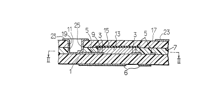
Fig. 1 is a fragmentary sectional view showing an essential
part of an embodiment of an electric component-mounted circuit board
in accordance with the present invention. Fig. 2 is a sectional
view taken along the plane of the line II-1I of Fig. 1. Figs. 3 to 9
are figures each showing a state of manufacturing step of the
embodiment shown in Fig. 1. Fig. 10 is a fragmentary sectional view
showing an essential part of another embodiment of the electric
component-mounted circuit board in accordance with the present
invention. Fig, ll is a fragmentary sectional view showing an
essential part of an embodiment of an electric component-mounted
circuit board in accordance with the present invention, the electric
component being a capacitor. Fig. 12 is a perspective sectional
view of an embodiment of a multilayered circuit board having a
circuit board in accordance with the present invention as a core
circuit board thereof.
BEST MODE FOR CARRYING OUT INVENTION
An embodiment showing the best mode for carrying out the
present invention is hereinafter described with reference to the
drawings. Fig. 1 is a fragmentary sectional view showing an
4
CA 02246405 1998-08-14
essential part of an embodiment of an electric component-mounted
circuit board in accordance with the present invention. Fig. 2 is a
sectional view taken along the plane of the line B - B of Fig. 1.
Figs. 3 to 9 are figures each showing a state of manufacturing step
of the embodiment shown in Fig. 1. The circuit board of this type
is a multilayered circuit board formed by so-called build-up
technique. Referring to Fig. 1, 1 is a board made from a rather
rigid insulating substrate, such as a glass epoxy substrate, a
phenol resin substrate, or the like. The circuit board 1 is formed
with a circuit pattern 5 including a pair of contact electrodes 3, 3
on the front surface, and also formed with another circuit pattern 6
on the rear surface. The circuit patterns 5 and 6 can be formed
either by etching a copper foil formed on the circuit board or by
using an electrically conductive paste. The electrically conductive
paste can be, for example, a mixture of conductive particles such as
silver, copper, silver-palladium or the like and a phenol or epoxy
resin binder. If the circuit pattern 5 is formed by etching the
copper foil, the surfaces of the contact electrodes 3, 3 are
preferably covered by such an electrically conductive paste as
described above. Fig. 3 shows the board formed with the circuit
patterns 5 and 6 on each surface.
The front surface of the board 1 is further formed with a
photoresist film 7 made of a photosensitive resin material such as a
phenolic novolak resin or an epoxy resin. The photoresist film 7 is
formed with an electric element forming hole 9 by lithography for
exposing a pair of contact electrodes 3, 3 and a hole 11 for forming
an electrically conducting through-hole afterwards. Referring to
Fig. 4, the photoresist film 7 is so formed that first, a
photosensitive resin material is applied on the whole surface of the
board 1, and dried to form an unexposed photoresist film 7', which
is before exposure. Then, the unexposed photoresist film 7' is
exposed through a mask with a previously determined pattern for the
electric element forming hole 9 and the hole 11 for forming the
electrically conducting through-hole (photolithography), or, instead
of the exposure, irradiation of the electron beams is performed
(electron radiation lithography). In this embodiment, a positive
CA 02246405 1998-08-14
photosensitive resin material is used that the solubility of the
', part where the light or the electron beam is applied increases and
the part becomes soluble in developer easily. In this embodiment,
the exposed or irradiated part is dissolved by wet etching using a
developer. Fig. 5 shows the state that the wet etching is
completed, where the photoresist film 7 is formed with the electric
element forming hole 9 and the hole 11 for forming the electrically
conducting through-hole. As seen in Fig. 5, a pair of contact
electrodes 3, 3 is exposed in the electric element forming holes 9.
The shape of the electric element forming hole 9 in this embodiment
is a rectangular as shown in Fig. 2. In practice, the board is
formed with a number of electric element forming holes 9 and a
number of holes 11 for forming the electrically conducting through-
holes. Also, if an inductor, a capacitor or the other electric
element is to be formed on the board 1, the electric element forming
hole 9 can be formed for each element.
An electric element 13 is formed by filling an electric
element forming paste in the electric element forming hole 9. (Figs.
1 and 6) In this embodiment, the electric element 13 is a resistive
element or a resistor, so that a resistive paste made of a mixture
of an epoxy or phenol thermoset resin and powdered carbon can be
used for the electric element forming paste. In this embodiment, a
resistive paste made of epoxy thermoset resin is used. When the
resistive paste is filled in the electric element forming hole 9,
the opening of,the hole 11 is covered with a mask or the like to
prevent the resistive paste from entering the hole 11. The board
with the resistive paste is then heated in a low-temperature
calcination oven to calcine the resistive paste to form a resistive
element for the electric element 13.
A protective film 15 is formed on the electric element
13.(Figs. 1 and 7) The protective film 15 made of a synthetic resin
is formed to cover the opening of the electric element forming hole
9 which is filled with the electric element forming paste material.
In practice, the protective film 15 is made by applying an epoxy
protective coating paint to cover the exposed part of the electric
element 13 and then calcined. The thickness of the protective film
6
CA 02246405 1998-08-14
15 is l0um to 100~m, practically, 20~m to 30um is preferable.
On the photoresist film 7 and the protective film 15, an
electrically insulating layer 17 made of a photosensitive resin
material as used for the photoresist film 7 is laid.(Figs. 1 and 8)
The insulating layer 17 is also formed with a hole 19 for forming an
electrically conducting through-hole by lithography. The hole 19
and the hole 11 are together forming a through hole 21. The
insulating layer 17 is not limited to one layered structure but can
be a multilayered structure, if necessary.
As shown in Figs. 1 and 9, a previously determined circuit
pattern 23 is formed on the insulating layer 17, and a through- hole
conductive section 25 is formed in the through-hole 21 to
electrically connect the circuit pattern 23 and the circuit pattern
5. The circuit pattern 23 and the through-hole conductive section
25 are formed of electrically conductive paste, for example, such as
a silver paste, a silver-palladium paste, or the like.
If trimming of the electric element 13, the resistive
element in this embodiment, is necessary, a trimming hole 27 may be
formed just above the protective film 15 when overlaying the
insulating layer 17, so as to expose at least part of the protective
film 15, as shown in Fig. 10. The case where the insulating layer
17 is made of the same photosensitive material as the material of
the photoresist film 7 as in this embodiment, the trimming hole 27
can be formed by lithography simultaneously with the other necessary
holes formed on the insulating layer 17. In case where the
insulating layer is made of an epoxy resin or the like, the trimming
hole 27 can be formed either by screen process printing or
mechanically by a drill or the other working tools after the
insulating layer 18 is formed.
Trimming can be performed in irradiating a laser beam to the
trimming hole 27. After the trimming operation, when the protective
film 15 is partially removed and a trimming groove is exposed, the
trimming hole 27 can be sealed up filled with a synthetic resin.
For forming an inductor as the electric element, the shape
of the electric element forming hole may be determined so as to
obtain desired inductance and the electric element forming paste may
7
CA 02246405 1998-08-14
be an inductor forming material such as a ferrite-resin. For
forming a capacitor as the electric element, the construction should
be as shown in Fig. 11, where a board 101 is formed with a circuit
pattern 105 including a contact electrode 103 which is to be a lower
side electrode of the capacitor. The board 101 further formed with
a photoresist film 107 having an electric element forming hole 109
for exposing the contact electrode 103. The electric element
forming hole 109 is filled with a dielectric paste and the
dielectric paste is calcined to form a dielectric element. Then, a
circuit pattern 123 including an upper side electrode 122 is formed
on the photoresist film 107 by an electrically conductive paste. In
this method, the printed capacitor smaller than a conventional
capacitor is easily formed on the circuit board 101.
Fig. 12 is a perspective sectional view of an embodiment
of a multilayered circuit board having a circuit board in accordance
with the present invention as an inner circuit board of it. In this
embodiment, the element which is the same as the element in the
structure shown in Fig. 1 bears the indication number adding 200 to
the indication number of the element shown in Fig. 1. In this
example, a protective film is not particularly provided on the
electric element.
INDUSTRIAL APPLICABILITY
In accordance with the present invention, the size of the
electric element formed on the circuit board can be greatly smaller
than a conventional element, which can consequently meet the needs
of the high density of the circuit pattern on the board. The
circuit board in accordance with the present invention can also be
used for a core board of a multilayered circuit board for achieving
higher density of the multilayered circuit board than before.
8