Note: Descriptions are shown in the official language in which they were submitted.
CA 02246500 1998-09-03
Doc. No. 10-79 CA Patent
Multilayer Thin Film Bandpass Filter
Field of the Invention
This invention relates to dielectric bandpass filters, and more particularly
to multi-
layer rnulti-cavity structures that reduce transmission ripple in the
passband.
Background of the Invention
1 o Optical interference, that modifies the transmitted and reflected
intensities of
light, occurs with the superposition of two or more beams of light. The
principle of
superposition states that the resultant amplitude is the sum of the amplitudes
of the
individual beams. The brilliant colors, for example, which may be seen when
light is
reflected from a soap bubble or from a thin layer of oil floating on water are
produced by
15 interference effects between two trains of light waves. The light waves are
reflected at
opposite surfaces of the thin film of soap solution or oil.
More importantly, a practical application for interference effects in thin
films
involves the production of coated optical surfaces. When a film of a
transparent substance
2o is deposited on transparent substrate such as glass, for example, with a
refractive index
which is properly specified relative to the refractive index of the glass and
with a
thickness which is one quarter of a particular wavelength of light in the
film, the
reflection of that wavelength of light from the glass surface can be almost
completely
suppressed. The light which would otherwise be reflected is not absorbed by a
non-
25 reflecting film; rather, the energy in the incident light is redistributed
so that a decrease in
reflection is accompanied by a concomitant increase in the intensity of the
light which is
transmitted.
Considerable improvements have been achieved in the anti-reflective
performance
3o of such films by using a composite film having two or more superimposed
layers. Two
different materials may be used in fabricating such a composite film, one with
a relatively
CA 02246500 1998-09-03
Doc. No. 10-79 CA Patent
high index of refraction and the other with a relatively low index of
refraction. The two
materials are alternately deposited to predetermined thickness' to obtain
desired optical
characteristics for the film. In theory, it is possible with this approach to
design multi-
layer interference coatings for a great variety of transmission and reflection
spectrums.
This has led to the development of many new optical devices making use of
complex
spectral filter structures. Anti-reflection coatings, laser dielectric minors,
television
camera edge filters, optical bandpass filters, and band rejection filters are
some of the
examples of useful devices employing thin film interference coatings.
to One particular type of interference coating is the bandpass filter, which
is
designed to allow wavelengths within a predetermined range of the desired pass-
band to
be transmitted, while a range of wavelengths on either side of the pass band
are highly
reflected. Ideally a bandpass filters should be square in its response; thus,
the transition
from the rejection regions to the passband should be as rapid as possible, or
expressed
15 differently, the slope or transition region should be as steep as possible,
while obtaining a
pass band region that is uniform having little or no ripple.
A classical three-cavity optical filter, has a transmission ratio of 1%
bandwidth to
SO% bandwidth of about 1.87. However, it is generally well known that that a
filter of
2o this type suffers from substantial ripple. It is also well known that as
the filter design is
modified to lessen ripple, the aforementioned ratio severely increases and
hence the filter
is far less square in its transmission response. An embodiment of the filter
in accordance
with this invention has a 1 % to 50% bandwidth ratio of only 1.97, wherein
transmission
ripple is substantially reduced. Thus the squareness of the optical filter is
only
25 compromised minimally.
Mufti-cavity filters have been manufactured for more than 40 years, and usual
approach of filter designers has been to simply anti-reflect equal length
cavity structures
to the substrate and the exit medium. However, this approach yields filters
with excessive
3o ripple in the passband. In an attempt to obviate this problem, the need to
modify the
cavity lengths was investigated by experts in the thin film field.
CA 02246500 1998-09-03
Doc. No. 10-79 CA Patent
P. W. Baumeister in a paper entitled "Use of microwave prototype filters to
design multilayer dielectric bandpass filters", published in Applied Optics
Vol. 21, No.
16, August 15, 1982, describes the use of a standing wave ratio technique to
match
reflective zones applying microwave filter synthesis.
C. Jacobs in an article entitled "Dielectric square bandpass design", in
Applied
Optics, Vol. 20, No. 6 March 15, 1981, describes the use of an effective index
approach.
A. Thelen in a book entitled Design of Optical Interference Coatings, McCrraw-
Hill
1o Book Company 1989, describes equivalent layers and other schemes to reduce
ripple.
However, the layer sequences developed from these methods are not considered
to be
general and do not apply equally well for different ratios of index of
refraction of the
multilayers.
15 Generally, procedures that result in high transmission, reduce the
bandwidth of
this transmission at the expense of poor slopes (i.e. a slow rate of change)
in the transition
to blocking. Since the irnprovernent in transmission outweighs the change in
slope,
additional cavities may be added to a filter to improve the slope.
2o In view of the limitations of the prior art, it is an object of this
invention to
provide a bandpass filter that overcomes many of these limitations.
Furthermore, it is an object of this invention to provide a banc~ass filter in
the
form of a mufti-layer, mufti-cavity structure that reduces transmission ripple
in the
25 passband, normally associated with other bandpass filters.
Furthermore, it is an object of this invention to provide a bandpass filter in
the
form of a mufti-layer, mufti-cavity structure that reduces transmission ripple
in the
passband and provides better slopes than those normally associated with other
bandpass
3o filter designs with reduced ripple.
CA 02246500 1998-09-03
Doc. No. I o-79 CA Patent
Summary of the Invention
The present invention is comprised of a multilayer film of alternating layers
of
two (or more ) transparent dielectric films with dissimilar indices of
refraction. The
invention utilizes anti-reflection from the filter structure to the substrate
and output
interfaces (if necessary ) These filters, in accardance with this invention
have extra half
waves added to various layers in selected cavities to provide three-quarter
wave layers.
Advantageously, the desired result, reduce ripple, is produced with virtually
any
to suitable materials that are transparent in the spectral area of interest.
In accordance with the invention, there is provided a bandpass filter
comprising:
an array of cavities including two outer cavities and one or more other inner
core cavities,
each cavity having a plurality of quarter-wave reflecting stacks comprising
layers of
15 material of alternating high and low refractive index, said plurality of
stacks beings
separated by a half wave layer of dielectric material, each cavity being
separated by
quarter-wave layer of low refractive index material, The improvement consists
of adding
half wave layers positioned in the inner cavities adjacent quarter-wave layers
to remove
ripple induced by the outer cavities.
In accordance with the invention, there is further provided, a mufti-layer
multi-
cavity filter comprising a predetermined a first group of cavities, and a
second group of
cavities, each cavity having a plurality of quarter wave reflecting stacks
comprising
layers of material of alternative high and low refractive index being
separated by a half
wave or multiple half wave layer of dielectric material, at least one of the
stacks in the
first group includes an additional half wave layer is provided in addition to
the quarter
wave layers for lessening ripple.
In accordance with the invention, there is provided, a bandpass filter having
a
3o plurality of cavities including two outer cavities and one or more other
inner core
cavities, each cavity having two quarter-wave reflecting stacks comprising
layers of
CA 02246500 2002-11-05
Doc. No. 10-79 CA Patent
material of alternating high and low refractive index, said stacks in each
cavity being separated
by a half wave layer or multiple half wave layer having three or less half
waves of dielectric
material, each cavity being separated from an adjacent cavity by quarter-wave
layer of low
refractive index material, wherein some of the quarter-wave reflecting stacks
include at least a
three quarter-wave layer and wherein three quarter-wave layers present in the
first outer cavity or
in the second outer cavity or in both first and second outer cavities are for
altering the slope of
the passband, and wherein three quarter-wave layers disposed in the inner
cavities are for
lessening ripple introduced by any three quarter-wave layers present in any of
the outer cavities.
In accordance with this invention, an optical filter is provided, wherein the
addition of a
half-wave layer to a quarter wave layer of a reflecting stack, changing the
effective index of the
stack of a cavity provides significant improvement in the reduction of ripple.
The following
figures illustrate a significant improvement in ripple reduction over standard
quarter wave
reflecting stacks.
Brief Description of the Drawings
Exemplary embodiments of the invention will now be described in conjunction
with the
drawings, in which:
Fig. la is a cross sectional view of a prior art bandpass filter ensemble;
Fig. 1b is a cross sectional view of a bandpass filter ensemble in accordance
with the invention;
Fig. 2 is a cross sectional view of a solid etalon filter in accordance with
the prior art;
Fig. 3 is a cross sectional view of a prior art quarter wave stack (QWS);
Fig. 4 is a cross sectional view of a prior art dielectric filter cavity;
Fig. 4a is a cross sectional view of a dielectric filter cavity in accordance
with this invention.
Fig. 5a is a cross sectional view of a prior art mufti-cavity filter;
Fig. 6 is a graph of transmittance versus wavelength of a five cavity filter
in accordance with
this invention (heavy line at 10 degrees incidence) and of the filter (light
line at normal
incidence);
CA 02246500 1998-09-03
Doc. No. 10-79 CA Patent
Fig. 7 is a graph of transmittance versus wavelength of a conventional six
cavity
structure (light line) and for a six cavity filter in accordance with this
invention (heavy
line; )
Fig. 8 is a graph of transmittance versus wavelength of a seven cavity filter
in accordance
with this invention ( wherein the heavy line illustrates an optical density
logarithmic
scale); and,
Fig. 9 is a graph of transmittance versus wavelength of three optical four
cavity filters,
the outer line being for a classical all half wave design, the inner light
line, full waves on
inner cavities, and the heavy line representing the response of three quarter
wave layers
1 o and half wave layers on the inner cavities.
General Information about Fitter Construction
Filters for wavelength division multiplexers and other communication industry
applications require very straight slopes with low loss and virtually no
ripple. Typical
bandwidths range from 0.5 nm to 100 nm for the wavelength range 1250 to 1650
nm.
There are many other applications for filters that would benefit from this
improvement in
technology that is provided by this invention.
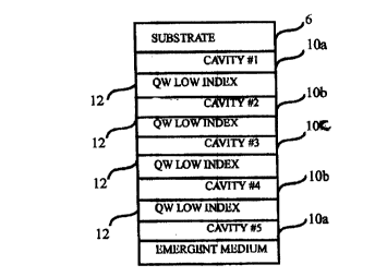
2o Fig. la is a diagram illustrating a conventional mufti-cavity optical
filter.
The simplest filter, shown in prior art Fig. 2, consists of two partial-
reflectors or
semi-mirrors separated by a half wave layer of transparent dielectric material
(similar to
an Etalon).
Turning now to Fig. 3, for all-dielectric filters, the partial-reflector shown
consists
of alternating layers of high and low index materials. The thickness of each
layer is
adjusted to be a quarter wave (QW) at the wavelength of the desired filter.
Each partial-
reflector (which may be comprised of only a single layer) is called a quarter-
wave stack.
The bandwidth of the filter is a function of the reflectance of quarter-wave
stacks in the
structure.
CA 02246500 1998-09-03
Doc. No. 10-79 CA Patent
Referring now to Fig. 4, a filter cavity, one of the most ubiquitous and basic
building blocks for all-dielectric interference filters, is shown. The cawity
is comprised of
two identical reflectors made from quarter-wave stacks separated by a half
wave (or
multiple half wave) layer, as is seen in Fig. 4. Cavities are deposited on top
of other
cavities, with a quarter-wave layer of low index material between, to sharpen
the slopes.
This produces a mufti-cavity filter shown in Fig. 5a.
From a practical point of view, the total number of layers to be deposited
controls
the number of cavities possible. At 0.3 nm bandwidth and greater, mufti-cavity
designs
1o are possible. Filters up to 10 nm bandwidth may be made easily with 3 or 4
cavities. For
greater than 6 nm, even more cavities may be necessary to achieve the slopes
for
blocking the transmission of unwanted wavelengths of light. These filters have
a large
number of layers. Surface area yield is small and 25 mm diameter may be
typical for the
narrower bands. Equal length cavities produce the best roll-off with the
broadest pass-
zones, but examination of the graphs for equal cavity filters demonstrates
that
improvement is needed.
Detailed Description of the Invention
2o Referring to Fig. lb of the invention, generally, the optional matching
layer is a
low refractive index material hawing a thickness of a quarter wave. However,
material,
thickness, and index of refraction of the matching layers) may be different
from that of
the low index material 12. The cavities l0a and l Ob and l Oc comprise
alternating quarter
wave thick layers of high and low index materials. Between the cavities is a
quarter wave
low index (L) material. The first material in a cavity l0a is a quarter-wave
high-index (H)
material and is followed by a quarter wave of low index (L) material. The
structure of the
cavity l0a is (HLHHLH); each layer indicating a quarter wave thick high or low
index
material. Thus, HLHHLH is considered to be a four layer structure, having a
half wave
layer HH of high refractive index material disposed between two layers HL,
each a
3o quarter wave thick of high refractive index material. Next, the low index
layer 12 is
disposed between each cavity l0a and/or l Ob that follows. The next core
cavity l Ob is of
CA 02246500 1998-09-03
Doc. No. 10-79 CA Patent
the layer structure HLLL HH LH. Hence, the core cavity lOb is considered to be
a five
layer structure, having a half wave layer LL added to the low refractive index
layer
before the spacer layer HH to reduce ripple. A cavity l Oc adjacent l Ob is of
the layer
structure HHHL 4H LHHH, wherein the spacer layer is a multiple (2) half wave
layer.
The filter is symmetric about the cavity 10c, having cavities 10a, and l Ob on
both sides of
l Oc.
The substrate 6 is transparent over the wavelength of interest and may be made
from a wide variety of materials including but not limited to glass, quartz ,
clear plastic,
silicon , and germanium. The dielectric materials for this application have
indices of
refraction in the range 1.3 to greater than 4Ø The preferred materials are
Magnesium
Fluoride (1.38), Thorium Fluoride (1.47), Cryolith (1.35), Silicon Dioxide
(1.46),
Aluminum Oxide (1.63), Hafnium Oxide (1.85), Tantalum Pentoxide (2.05),
Niobium
Oxide (2.19), Zinc Sulphide (2.27), Titanium Oxide (2.37), Silicon (3.5),
Germanium
(4.0), and Lead Telluride (5.0). Other dielectric materials would serve as
well.
After establishing the number of layers in each cavity, in accordance with the
teaching of this invention, the design of the filter is easily accomplished
with the aid of a
commercially available computer program with optimization routines (for
example,
2o TFCaIcT"' by Software Spectra Inc.). Design recipes are entered into the
program and a
spectral response is calculated. When the design with the proper size cavities
is selected
to match the required nominal bandwidth, optimization of the filter
transmission is
performed for the matching layers. A designer selects from a choice of
materials to use in
a quarter wave match or may choose to use the same low index material with
thickness
adjustments to accomplish the matching.
The filter of Fig. 1 b includes of an array of cavities, each separated by
quarter
waves of low index material. Additional half waves are attached to quarter-
wave layers
in the outer stacks yielding three-quarter wave layers to improve the slope.
However, this
3o introduces ripple. Nevertheless when the slope is satisfactory, the ripple
is reduced by
8
CA 02246500 1998-09-03
Doc. No. 10-79 CA Patent
adding more half waves to quarter-waves in the inner stacks thereby yielding
three-
quarter wave layers.
Fig. 4a shows a cavity in accordance with the invention wherein extra half
wave
layers are added to high index quarter wave layers yielding three quarter wave
high index
layers.
When the general attributes of the filter are satisfactory, the position of
the added
multiple waves may be tested for angular sensitivity. Altering the positions
slightly may
to provide vastly improved filter properties for a variety of angles of
incidence.
The following graphs will illustrate that the transmission response as a
function of
wavelength is shown wherein ripple is significantly reduced from a same filter
absent the
extra half wave layers in the inner cavities.
Referring now to Fig. 6, a response is shown (in heavy outline at 10 degrees
incidence) of a five cavity diverse filter with extra half wave layers added
and for a same
filter (shown in light outline at normal incidence). As is evident, ripple is
significantly
low in both of these graphs.
The filter structure with the extra half wave layers is as follows:
(HLHLHL3H2L3HLHLHLH) L (HLHLHLHL 2H LHLHLHLH) L (HLHLHLH 3L 4H
LHLHLHLH)L (HLHLHLHL 2H LHLHLHLH) L (HLHLHL3H 2L 3HLHLHLH)
In Fig. 7 a six cavity diverse filter is shown wherein the conventional filter
(light
outline) has excessive ripple. As is evident from the response shown (heavy
outline) the
ripple is essentially removed by the cavity having the following structure:
(HLHLHLH 2L HLHLHLH) L (HLHLHLHL 2H LHLHLHLH) L ( HLHLHLH 3L 2H
LHLHLHLH) L (HLHLHLH 3L 2H LHLHLHLI-~ L (HLHLHLHL 2H LHLHLHLH) L
(HLHLHLH 2L HLHLHLH)
9
CA 02246500 1998-09-03
Doc. No. 10-79 CA Patent
Fig. 8 shows the transmission profile of a bandpass filter having seven
cavities.
Ripple is reduced to approximately 1% or less. The heavy outline shown is a
graph of the
output response using a logarithmic optical density scale:
The filter's quarter wave layers are arranged as follows: (HL HH LH) L (HLH LL
HLH) L (HHHLH LL HLH) L (HHHLH LL HL~ L (HLH LL HLHHH) L (HLH
LL HLH) L (HL HH LH ).
The index of refraction of the substrate and the emergent (or exit) medium
will
to affect the ripple. To reduce ripple to a minimum, it may be necessary to
match the filter
structure to the emergent medium. For example, when the refractive index n of
the
emergent medium is between 1.44 and 1.8 a quarter wave layer of the low index
material
(for a low index material with an index of approximately 1.48 or less) may
provide
suitable matching. For indices of refraction greater than approximately 1.8 or
less than
approximately 1.44, layer changes are necessary between the medium and the
filter. This
particular problem is well known and has been addressed by those proficient in
the art.
Fig. 8 demonstrates the effect of matching a ftlter with an exit medium. For
any
substrates and exit mediums structure changes next to the mediums enhance the
performance of the filter such that the indices of the substrate and output
medium are not
obstacles.
Fig. 9 shows a graph of three output responses at 20 degrees for three four-
cavity
filters having different inner cavity layer structure. In Fig. 9 the light
outer line depicts
the response for a classical 4 cavity filter of the form (HLHLH LL HLHLHL~1.
The
inner light line shows a modification to the classical filter as taught by
Thelen wherein a
full wave layer is used on the inner cavities. It is noted however, that these
responses are
not desirable and significant ripple is shown as present at 20 degrees angle
of incidence.
The response illustrated by the heavy line in the figure shown a significant
improvement,
wherein three-quarter wave layers and full wave layers are used in the inner
cavities. The
3o form of this filter in accordance with an embodiment of this invention is
as follows:
to
CA 02246500 1998-09-03
Doc. No. 10-79 CA Patent
(HLHLH LL HLHLHL) (HLHL 3H 4L HLHLHL) (HLHL 3H 4L HLHLHL) (HLHLH
LL HLHLHL).
Of' course numerous other embodiments and applications may be envisaged,
without departing fiom the spirit and scope of the invention.
11