Note: Descriptions are shown in the official language in which they were submitted.
CA 02246776 1998-09-08
METHOD AND CIRCUIT CONFIGURATION FOR POWER
CONTROL WlTH LOW SWITCH~G SURGES FOR
ELECTRICAL LOADS
5 The present invention concerns a method and a circuit configuration for
power control with low ~wilchillg surges for electric loads that are divided
elecl~ically into at least two par~al loads, whereby to achieve the required
hefltin~ power they are distributed among the partial loads largely
Imifonnly in a certain power range.
When electric loads on a power supply system, such as a public a.c.
system, are varied, ch~nges in line voltage occur due to the impedance of
the supply lines. These voltage ch~nges ~also known as flicker) are
perceived as problematical by people in certain frequency/voltage ranges
15 and must therefore be kept within narrow limits ~flicker level) according to
IEC 1000-3-3 and IEC 1000-3-5 standards. If electric loads such as he~stin~
systems must be switched on and off freqllent1y to achieve a good control
characteristic, only limite~l load ch~nge~ can be switched per unit of time.
This is achieved by dividing the total load into individual, sep~ale, partial
2 o loads which are not switched at the same time or by dividing the total load
into power stages.
German Patent No. 3,601,555 C2 describes a controlling element for
stepwise power ~wil~ g of an electlic flow-type hefltin~ element as a
2 5 function of power ~lem~n~l, wherein for power control in a cycle
compri~in~ multiple system full waves, system half waves are more or less
switched through to at least one heating el~m~nt, and the same number of
positive and negative half waves occur in the cycle. Therefore, several
di~renl control signal p~lt~,. ..~ which switch th~ough corresponding
3 o system half wave p~lle~ .~s to an electric h~l ing eleme~t as a fu~ction of the
power dem~n~l are stored in an electronic memory, with each control signal
of the respective pattern ~wil~hillg through a halt' wave or several
successive system half waves to the electric heating element Each system
half-wave pattern is designed so that its short-term flicker level is below
3 5 the i~ r~,~nce limit, and the system half-wave ~ are grad~late~ with
regard to electric power in that they comprise a di~clll number of half
waves switched through. For ~wiLching int~nediate power stages in a
cycle c~mpri~in~ multiple system half-wave pii~ --C7 system half-wave
CA 02246776 1998-09-08
pattern~ of dirrelel~l loads are switched in succession. The object achieved
according to the patRnt spec-ifi~tion is that the required freedom from
flicker in comhi1l~tion with sensitive control of hefltin~ power can be
achieved by stipulating li~le.~l system half wave patterns, each stored in
5 direct-voltage-free control signal pflttern.s, and by processing them in a
fixed cycle.
German Patent No. 3,726,535 Al discloses a method of power control with
low ~wi~ g surges for electric loads, where the h~tin~ loads are divided
0 electrically into at least two underloads, and the underloads of each load,
optionally in at least three main power stages in a series connection, can be
~ltern~tely switched to an a.c. system individually or in a parallel
connection. Starting from one of the main power stA~es, it is switched to
the next lower main power stage during at least one half wave in each cycle
5 in a continuously l~pcr~ p cycle of at least two a.c. ~lf waves. The
~wil~,hing cycles used there each have a leng~ of six half waves, which are
switched according to power ~lemAn~
German Patent No. 10,504,470 Al describes an elec~ic flow-type h~Atin~
20 element where the grfl~duAtion~ in he~tin~ power are achieved in a lmown
way by apl)ropliate m~s~in~ out of partial areas of the usually sinusoidal
heAtin~ current. The heating current is switched in the zero crossings. With
this electric flow-type h~flting element the total h~ti~ current is divided
among various hPAtin~ el~ment~ and the individual h~fltin~ elementc each
25 have a di~re,~l nonlin~l h~Atin~ power. By means of a control circuit7 the
respective he~tin~ power is switched to as many he~ting elements as
possible. The heating power is gradu~te~l in 1/3 steps (0/3, 1/3, 2/3 or 3/3)
of the nominal hefltin~ power. The hefltin~ power or h~Atin~ current is
switched through to the hPlAtin~ elementc during six system half waves,
3 o where a corresponding number of half waves, corres~ lin~ to the h.ofltin~
power, is switched as already described in Unex~mined German Patent No.
3,726,535 Al. Thus, at 1/3 power, the first and fou~th half waves are
switched, at 2/3 power the second, third and fourth and fi~ half waves are
switched, and at 3/3 power all the half waves are switched. To achieve the
3 5 desired power, ~e individual he~tin~ stages which have a di~ele~ nQmin~gl
power are switched in succes~ion, paying ~ttenti~ n to the fact that all three
CA 02246776 1998-09-08
loads are allocated lmif~rmly with a hf~tin~ stage before dhe next higher
hPfltine stage is col~lccled at a partial load.
With dhese known load sharing methods, only one load ca;n be switched
5 direcdy. The load is distributed by fixed, power-proportional connection of
par~al loads and regulation over a parti~l load. With a hefltine system,
especially involving the hP~ting of air, for example, for hot air welding
systems, or other welding equir)m~Pnt and hot air eq1lirmPnt~ this leads to
di~.cnl le.~ s in the ~l~ere.ll load ranges, because the power
0 output ofthe partial loads may differ by up to 100%. Great tempe.alule and
load diJT .~nces lead to m~teri~1 stresses and premature aging of hP~tin
element~.
According to the state of the art, power stages can be achieved by
15 controlling individual half waves, where this pulse pattern control can be
used only for loads up to ~pluxilllately 2.5 kW on the basis of the
standard for the flicker rate. If larger loads must be controlled, mostly
complicated and ex~n~ive electric ~ir.iuil~ are necessary. As a rule, the
pulse patterns are set r~n~lntn1y in sl1ccession according to the power
20 dem~n~l7 so the swil~hillg surge load to be expected in the system cannot be
dele~ clearly.
Therefore, the object of the present invention is to propose a possibility for
con~olling loads that p~ flicker-free switching within the given
2 5 standard of a mn1titvdP of partial loads, where the par~ial loads are brought
onto load unifo~nly at any power dem~tld
This object is achieved according to the present invention by a method
having the feal~es of the main claim and by a circuit configuration having
30 the realu.es of Claim 8. A(l~ition~l embo~liment~ of the method can be
derived from the subclaims based on the main claim.
With the method according to the present invention, three se~alale pulse
pattern sequences A, B and C are formed from three successive system half
35 waves which form a so-called pattern period, where said pulse pattern
sequences correspond to the ~ecli~e system half waves and their
CA 02246776 1998-09-08
negative half waves are rectified. Each pulse pattern sequence A, B and C
switches at least one partial load over a pred~ led period, which is
referred to as the PWM: period, where each pulse pattern sequence A, B
and C ~ilches a ll.~ of one third of the non-infll power to a partial
5 load, referred to below as the pulse pattern power, according to the
ms.xilt.~ . number of pulses per PWM period. Each partial load is thus
switched by one or more pulse p~ttern sequences A, B and C according to
the total power dç~n~(l so that at an output of 100% of the n~min~l power
of the partial load, the partial load receives the Ill~Yi.ll~ l pulse pattern
o power of each pulse pattern sequence over the entire PWM period.
Accordingly, the respective partial load receives one pulse pattern sequence
at 1/3 of the nomin~l power and two pulse pattern sequences at 2/3 of
nominal power. Fu~ ore~ the respective partial load is s~,vitched over a
preselectable PWM period by pulse width mod-l1ation (PWM) of at least
5 one pulse pattern sequ~nce according to the total power dem~nd through
the number of pulses of the res~e~ e pulse pattern sequence A, B and/or
C during this PWM period. Through such pulse width mod~ tion which
can be performed essçnti~lly like any pulse pattern sequence, the
intçnnediate values between the above-mentioned 1/3, 2/3 and 3/3 stages
20 can be set. Due to the division among the three pulse patt~rn~ one third of
the nominal power is switched to the r~s~e~ e partial load over a PWM
period of one pulse pattefn In the actual ~wilchillg operation of each pulse,
however, the full nf min~l power is always switched to the partial load.
Swilchillg is always done at 1/3 of double system frequency, whereas 1/3
2 5 of the half wave frequency is switched at one pulse pattern sequence. The
PWM period and the half-wave frequency are synchronized with the
system frequency. It is also possible to subdivide a pattern period into
multiples of three, but the basic princirle is the same and can be reduced to
three. On the whole, flicker and the l~l~c~alule flnct~l~ti~n~ of individual
3 o partial loads are red~ed by the longer period fluchl~ti~n~.
According to another embo~liment of the invention, the number of
~wilcl~g stages of the partial loads can be adjusted through the number of
pattern periods. Thus, the accuracy of the above-mentioned int~nediate
3 5 values which are produced by PWM can be influenced.
CA 02246776 1998-09-08
According to another especially lJlerell~d embo~irnent pulse width
mod~ tion is pe. rO....ed with only one pulse pattern sequence, for
example, pulse pattern sequence A, where the pulse pattern sequence can
be ~wilched to any desired partial load. On exceeclin~ the m~Y ;1~ .l, pulse
5 pattern power of this pulse pattern sequence A, B and~or C, the next free
pulse pattern sequence, for example B or C, is switched with m;1x;.,,l,...
pulse pattern power, and the number of pulses of pulse pattern sequence A
is re(hlce~l according to the total power ~lem~l This is accomrli~hed such
that the re~pc~;live pulse pattern sequence receives the above-mentioned
0 mfl~ .... pulse pattern power (one third of the nomin~l power) of a partial
load, and PWM is p~forrn~d agam with the re(hlce~l pulse pattem sequence
A. This pe~,ils fine gradations in power and distlibution to individual
partial loads. To always distribute the power ~ iformly among the
individual partial loads in setting the required power, according to another
5 especially l~re~l,ed embo~ t the next free puls~e pattem sequence
switched to another partial load is switched with mi~;...l-". pulse pattern
power to the par~al load. The power to be switched is already distributed
to various partial loads within one PWM period.
20 With regard to the simplest possible circuit design and lowest possible
~licker rate, according to anot;her embo~liTnent the pulse pattern sequences
and their comlection to the partial loads are interch~n~ed in cycles in order
to set the required tot~l power. This is accomplished such that first all the
pulse pattern sequences A, B and C are allocated with ~ x;."l.,.. pulse
2 5 pattern power before a pulse pattern sequence A, B or C is again allocated
with connection of ln~Y;.,.~... pulse pattern power.
To further improve flicker rate, pulse-width-modulated pulse pattem
sequence A is ~ssigned to the next partial load, not yet pulse width
3 o mo~ te~1 in the following PWM period. Thus, the PWM in pulse pattern
sequence A is routed from one partial load to the next partial load, and
consequently each individual partial load in successive PWM periods
receives at least part of the required total power. Consequently, there are no
great power diLre~c~ces between the individual partial loads. In addition,
3 5 this possibility pt~ a reduction in flicker rate and reliable compliance
with the required flicker rate.
CA 02246776 1998-09-08
The latter is improved further in particular due to the fact that according to
another embo~liment the PW-mo~nl~tecl pulse pattern sequence is ~ssiened
to the individual partial loads in sllccession with cyclic exch~nge, and at
5 the same time the PW-mo~hl1Pte~l pulse pattern sequences of two successive
PWM periods are a~ranged between the two PWM periods, symmetrical
with the middle. This means that a PW-mo~ ted pulse pattern sequence
A at the beginnin~ of a PWM period, for example, is ~ranged at the end of
this pulse pattern sequence, ~ ored in the next PWM period toward the
0 middle between the two PWM periods. As already explained above, the
pulse pattern sequence A in the first PWM period has changed from one
partial load to the next partial load in the next PWM period. This is always
contin~led bclween two sllcces.sive PWM periods, so that with even-
numbered partial loads, a system period, after whose end the seqnence of
15 the load connection by the individual pulse pattern se(lllçnces begins again
from the beginning is derived from an even number of partial loads used,
and with an odd IlUlulx;f of partial loads, the system period is derived from
double the number of partial loads. This prevents ~~ ed flicker in a
special way, because no s~,vitching operation that would cause flicker for
20 the line voltage is carried out when the PW-mod~ ted pulse pattern
sequence is switched from one partial load to the next. One partial load is
merely switched off and at the same time the next parlial load is switched
on. Due to the cyclic exchqnge, the same process is also ca~Tied out with
the pulse p~ receiving m;~x~ ..,. pulse pattern power and the p~rtial
2 5 loads ~si~ned to them in ~l~m~1ion.
The circuit configuration according to the present invention has a pattern
generator for generating ~ree separate rectified pulse pattern sequences (A,
B, C) from three sllccessive system half waves and a controlling device per
3 o partial load to be controlled. At least one controlling device has at least one
pulse width mo~h~ on genc.al~l (PWM generator) which generates a
corresponding nlltnber of pulses of the respective pulse pattern sequence A,
B and/or C over a ~ed~h ed period (PWM period) corresponding to
the total power d~n-nnd, and each controlling device has a corresponding
35 number of colllp~lurs, where the total number of PWM gencldlo-~ a~d
COlll~ vl:i iS three per controlling device, and each PWM generator or
CA 02246776 1998-09-08
co~ alor switches a m~ of one third of the nominal power to a
partial load, and one of the pulse pattern sequences A, B or C can be
switched with the n~i~xi...~l.., number of pulses per PWM period over each
col~aLur in conjunction with the pattern generator over the duration of
5 the PWM period. ]D ~ddition~ the circuit configuration has logic units for
applying at least one pulse pattern sequence to the respective partial load
according to the tot~ll power dçm~nd over a preselectable PWM period
through the number of pulses of the res~ iLi~e pulse pattern sequence A, B
and/or C during this PWM period, and it has a controlling element for
10 activating the generators and co~dlalol~.
The invention thus makes it possible to control a plural-ity of single-phase
and three-phase loads with low switching surges, where the cu~ l surge
load of the system due to the connectable loads can be calcl~lflted
15 accurately in advance. Through an ~l)ro~liate choice of the individual
~wilchillg stages and the pulses per unit of time, a load-~ n(l-comr1i~nt
Opti~ for the given application case can be implçnl~ntecl reliably, taking
into account the l-,spe~ e flicker standards. Power L divided ~.;r~...1y
among the partial loads, but it is no longer necessary to gcnclalc a new
20 control method for each new power stage. The pa~tial loads need not
necessnrt1y be equal, but equally large partial loads are he1pfi11 for the
flicker rate. There is the option of a modular hookup. If another partial load
is generated, it can be applied to the overall circuit system with only minor
ch~t g~s7 without altcring the principle of the method. The basic principle
25 can also be applied to three-phase loads (in a star connection or a delta
connection), where the particular features of the three-phase system must
be taken into account especially with delta-con~ected loads in a m~nner
with w_ich those sl~illed in the art are f~mili~r to prevent any imb~1~nce in
the system. Wi~ multiple loads, star-connected loads behave like single-
3 o phase loads with regard to one phase. When using a circuit configurationorientçd for two partial loads, this can be used for two single-phase loads
or for three-phase loads for control with low ~wil~hillg surges. This control
is especially ad~ eous with (air) heaters, bec~nee all the partial loads
are heated unifo~mly, and therefore the air temperature is not subject to
35 great fl1~,tlfl1ione ~om one partial load to the next. In addition, the
windin~s are under low stress due to low temperature ~ erences due to the
CA 02246776 1998-09-08
~ iro~ control. At high powers, it is no longer necessary to make such
high dem~ le of the h~tin~ coil.
The present invention is explained in greater detail below on the basis of
embof~ in combin~ti~n with the acco~ jing drawings, which
show:
Figure 1: the pulse pattern division based on the system frequency;
0 Figure 2: a pulse pattern for two loads with di~e~ power
~lçm~n~ls;
Figure 3: a pulse pattern for three loads with dirrelcl~l power
d~m~n~ls and with a dirr~lcl-l number of pattern periods
per PWM step in comparison with Figure 2;
Figure 4: (a) the distribution of the power dem~n~led to co~ alor
stages; (b) the pulse duty factor for a PWM ~wil;hillg stage
and (c); and [sic]
Figure S: a circuit configuration for two partial loads.
Figure 1 shows the pulse pattern division with an a.c. system W and pulse
pattern sequences A, B, C ~si~ned to the half waves of the a.c. system.
2 5 The respective partial loads are controlled by means of these pulse pattern
sequences A, B and C. Each pulse pattern se~lence m;ly be ~signed to one
or more partial loads to inflllçnce their switching operation. In the
following embo~li.,.e~l!i, three system half waves and their ~~signed pulses
of the individual pulse pattern sequences A, B, C form one pattern period.
Figure 2 shows the pulse pattern over essçnti~lly two PWM periods for
four dirr~c"l load stages with 8%, 18%, 33%, 60% and 93% of the total
nominal power of the two partial loads. In this embo-limçnt eight
~wilclli~g stages were established per PWM period. At a m~x;..,~ power
3 5 of 33% (= 1/3~ of the nomin~l power of a p~rtial load, it follows from dlis
that a~r~x;...~tely 4~/O ofthe nomin~l power can be switched per switching
CA 02246776 1998-09-08
stage (33% 8 = 4~/O). In addition, one pattern period (= 3 half waves) per
PWM ~,wilching stage [is] selected. The number of available half waves
within one PWM period is obtained from the following form
5 number of switching stages x (number of pattern periods per
~,wilchil~g stage x number of
waves per pattern period).
In the embodiment according to Figure 2, this yields 24 half waves 8 x (1 x
10 3) within one PWM period. In this embo-lim~nt each half wave is
desi~n~ted with the letters A, B or C for simI)lification. Since there are two
loads, and thus there is an even t~nmber of loads, a total period consists of
two PWM periods. After the total period, the process begins again from the
beg1nnin~ For illustration purposes, the power increase obtained by
15 connecting a pattem for the respective partial loads is given for each
pattem period. The second pattern period is l--nluled to the first pattern
period, so that for the second pattem period accordingly, the ~wilchillg
stage values decreasc toward the end of the second pattem period. The
connection of the respective pulse of the pulse pattern A, B or C is
2 o represent~d by x's in this diagram.
In the embo(limPnt~, pulse pattern A is still pulse width mod~ te l, while
the other pulse patt~rnS are either switched on complet~ly or switched off
during the other pulse p~le. ..c over a PWM period. l)ue to the connection
2 5 of a pulse p~ltern such as B, to a partial load over the entire length of the
PWM period, the partial load receives 33% of the n/ mitul power during
this period of time.
To set a desired power d~m~n-l7 the required power must be distributed to
30 the individual parffal loads so that only one pulse pattern A, which is
assigned to a partial load, is pulse width modnl~ted7 while all other pulse
p~ "c are connected over the entire PWM period. On the e~mple ~,vith a
power dem~nd of 18%, this yields the full connection of the second partial
load by means of pulse pattern B during the first PWM period and the
3 5 connec1ion of ~e first pa~al load by me~ns of pulse patte~ A only duling
the first switching stage. This gives on lhe whole a power of 37%;
CA 02246776 1998-09-08
- 10-
distributed to two loads (average), a total power of a~roxi~..fltely 1~% is
calcnl~ted from this. After the first PWM period, the secorld partial load is
allocated with pulse pattern A which is pulse width mo~lnl~te~l while the
first partial load is allocated completely with pulse pattern B. This cyclic
5 exch~e and millo~ g at the middle between the two sl~ccessive PVVM
periods serves to reduce flicker rate because it is imrossible to detect on
the system side that one partial load has been switched off and the other
partial load is ~whcl~d on jnste~q~l and it also serves to achieve a l1nif~rm
distribution of power to the partial loads for the pu~pose of cor~inl1Qus
lo he~ting After the second PWM period, the system pe¢iod is ended and the
process begins again from the start. This principle is implçmente~l in all the
power (l~n~ ,1cs illustrated.
At a power dem~nd of 8%, only the first partial load receives the pulse
15 pattern A in the first PWM period with pulse wid~h mo~ tion The
change to the second partial load then takes place in the second PWM
period. The total power is 16% / 2 = 8%.
At a power dem~n~l of 33~/O, pulse pattern sequence C is switched fully to
20 the first partial load, and pulse pattern sequence B is switched to the
second parti~l load in this embo~liment After the end of one PWM period,
the ~si~...e.~l of partial loads to the pulse pattern sequences ch~nges as
shown in the figure.
2 5 At a power demfltl-l of 60%, the second partial load is completely allocatedwith pulse pattern sequence A and pulse pattern sequence B during the first
PWM period, which yields a partial load allocation of 66%. The first
partial load is completely allocated wi~h pulse pattern sequence C, and
PWM is performed at pulse pattern sequence A, yielding 20% allocation of
3 o the first partial load. This gives a total of approxima~ely 53% for the first
partial load, so that this yields an a~plo~;..,~te total load of 60% ((53% +
66%) 1 2). After the end of the first PWM period, the above-menli-)necl
mill~ling and reversal of connection ale pc.ro~ ed. Likewise wi~ each
~d~ Qn~1 PWM period.
CA 02246776 1998-09-08
Similarly, a total power of 93% is obtained from the pulse pattern
sequences shown in Figure 2. The second partial load is then allocated
100% during the first PWM period, while the first partial load is allocated
66% by pulse pattern sequences B and C and 20% by PW-modnl~tel~l pulse
5 pattern sequence A. This yields approxim~tely 93% for the total load
(186% / 2).
Like Figure 2, Figure 3 shows a pulse pattern, but with three loads. In
addition, in this embodim~nt two pattern periods per switching stage were
10 selected. Furthenmore, the switching stages for pulse width mod~ tion
were also set at two, so this yields a~rnx;."ately 16% per switching stage
(33% / 2). Consequently, one PWM period has 2 x (2 x 3) = 12 half waves.
In this embo~ ent~ shown in Figure 3 for illustration purposes, three
power d~m~nd.s of S~/O, 45% and 83% were selected. Just as before, pulse
15 width modulation is performed only with pulse pattern sequence A,
switching as described above from one pa~tial load in the first PWM period
to the second paItial load in the next PWM period and then to the third
partial load in the t~ird PWM period. Here again, ~wilchillg pulses of the
pulse pattern sequence of two s~lcces~ive PWM periods are symmetrical
20 with the middle of two s~lcce~sive PWM periods in order to obtain
~wilchil~ values that are favorable for the flicker rate. Owing to the odd
number of loads, six PWM periods are necess~ry for a system period until
the cycle begins again from the start. Owing to the selection of the number
of pattern periods, a pulse pattern sequence with two pulses must be
25 switched for the smallest power value. During the first PWM period, the
other pulse pattern sequences B and C remain switched off, so that the
pulse pattern sequence A occupies a power of ~)rox;...~tely 16% on
partial load 1, while the other pulse pattern sequences occupy 0% on the
two other partial loads. The average of this yields a~p-o,~ ly 5%.
The situation is similar with a power dem~nl1 of 45~/O, where the first
partial load is allocated with the complete pulse pattem sequence A in the
first PWM period, i.e., in ~is case there is no PWM here. The second
partial load is completely allocated wi~ pulse pattern sequences A and B,
35 and the third partial load is completely allocated wi~ pulse patterr
sequence C wi~in one PWM period. This yields a 33% allocation of the
CA 02246776 1998-09-08
first partial load, 67% of the second partial load and 33% of the third
partial load, yielding a total value of apt)rox;~.-fltely 44% for the three
loads. After the first PWM period, there is again a cyclic exchsng~ and
llf.~ g with respect to the middle between two successive PWM periods,
5 as explsirled le~c~ dly above. However, due to the full allocation of the
pulse pat~ern sequences, the UlLI1'V1~g iS not manifested as clearly here as
in the example with S% power d;~tl&~n(1 In the second PWM period, pulse
pattem sequence A is switched to the second partial load, while pulse
pattern sequence C, which was o1i~infl11y switched to the third partial load,
10 is now switched to the first partial load. Accordingly, pulse pattern
sequences A and B, which were originally switched to the second par~ial
load, are now ~wilched to the third partial load. This cyclic exch~n~e is
conlinlle~l from one PWM period to the next PWM period.
15 The power dem~n~l of 83% in Figure 3 is obtained accordingly, with an
allocation of 66% in the first PWM period of the first partial load from
pulse pattem sequ~nces B and C and 16% for the PW-m-d~ te~ pulse
pattern sequence A, 100% for the second partial load and 66% for the third
partial load from pulse pattem sequences A and C. This yields a total of
20 248% ((66% + 16%) + 100% + 66%), which is a~ru~ tely 83% when
divided among three loads (248% / 3). In the subse~lent periods, there is
again a cyclic eYch~g~ of pulse pattern sequences among the partial loads.
One system period is conclnded after six PWM periods.
2 5 For implemçnt~tion of the method according to the present invention, the
detn~nded power is divided in Col~ al~Jr stages (C~J~ JC~ O1~)~ and the
individual co~aral~l~ are always graduated in uIIiform power stages and
remain active up to 100% power. The number of COL~ lO1S depends on
the division of the load, wi~h the number of colllpa.a~l~ obtained from the
3 o following equation:
number of co~ a~ = 3 x (number of par~al loads) - 1.
Figure 4a shows a diagram illustrating the division of the required power
3 5 LA among five CO~ lols which are necessary wi1h two pa~al loads. It
can be seen here that col~ alor I is connected at 17% and remains
CA 02246776 1998-09-08
connected over the full power ~l~mfln~l The situation is similar for the other
co~ t~rs II, III, IV and V.
Figure 4b shows the pulse duty factor T for a PWM switching stage, also
with two loads, with regard to the power demqnd LA as an ex-qmple.
Synchronized with the system frequency, a PWM having the following
p~ lies is applied:
1. The resolution and the smallest discrete step are 2/3 of the system
0 frequency.
2. The f~xed period length is an integral divisor of the system
frequency by tbree.
3. The period is synchronized with the system frequency.
4. The PWM is linked to a pattern (A, B or C).
5 5. Optionally either the even-numbered PWM periods are first
cnnn~octed and then disconnected and then in the odd-nllmbered
PWM periods first the off component and then the swi~ g
component are driven or vice versa. Thus the pulse duty factors
between the ~wilclling component and the off component are the
same in the even-numbered and odd-numbered PWM periods, as
already shown in Figures 2 and 3 and explained above.
6. The pulse duty factor (ntodnl~tinn) of the PWM depends on the
number of partial loads to be controlled. ~f lnnl*ple, s~pa.~lely
driven power controllers are used, this yields a pulse duty factor, as
2 5 shown in the figure with two loads, of: power dem~n~l - 3 x nunlber
of power controllers.
Figure 4b shows that at a power dem~n~l of 17%, the pulse duty factor is
100%, i.e., at this power, a ~w~nl pulse pattern seqllence is completely
3 o switched to a partial load.
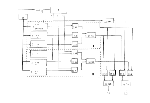
Figure 5 shows a block diagr~m of the design of a control circuit for two
loads Ll and L2, which are opcl~led as power controllers over bidirectional
triode thyristors (not shown), for exarnple. The system frequency of the a.c.
3 5 system is picked off and sent over a pulse former 1 with a double system
frequency to a pattern generator 2 and with 2/3 the system firequency to a
CA 02246776 l998-l2-02
- 14-
PWM generator 3. Comparators K I to K V according to Figure 4a are
parallel to PWM generator 3. Thus, number 4 denotes comparator K II,
which connects at 1/3 power, number 5 denotes comparator K IV which
connects at 2/3 power, number 6 denotes comparator K I which connects at
1/6 power, reference number 7 denotes comparator K III which connects at
half power, and reference number 8 denotes comparator K V which
connects at 5/6 power. The output of PWM generator 3 together with
output A of pattern generator 2, which [generates] pulse pattern sequence
A, is applied to an AND element 9. The output of comparator K III, which
l0 is designated with number 4, together with pattern sequence B delivered by
pattern generator 2 at output B, is applied to AND element 10, and the
output of comparator K IV, designated with reference number 5, together
with pulse pattern sequence C delivered at output C of pattern generator 2,
is applied to AND element 11. The outputs of the AND elements are linked
15 to OR element 15 and sent in parallel to an AND element 18 or 20. The
situation is similar with comparators K I, K III and K V, which are
designated with reference numbers 6, 7 and 8, which are applied together
with pulse pattern sequences C, A and B to AND elements 12, 13 and 14.
The outputs of these AND elements 12, 13, 14 are sent to an OR element
20 16, and its output is applied in parallel to AND elements 19 and 21. To
implement the cyclic exchange described above, a signal of PWM
generator 3 which changes every second PWM period is applied to an
inverter stage 17, and its output signal is applied to AND elements 19 and
20. In addition, this signal delivered by PWM generator 3 is sent without
25 inversion to AND elements 18 and 21. The outputs of AND elements 18
and 19 are linked via OR element 22, and the outputs of AND elements 20
and 21 are linked via OR element 23, and the respective outputs are sent to
a corresponding load controller for the respective load. By means of
controlling element 24, the power demand is sent to PWM generator 3 or
30 comparators 4 through 8, which are activated accordingly.
As already explained in conjunction with Figures 2 and 3, PWM
modulation is performed only with pulse pattern sequence A and is linked
to AND element 9. Above a power demand of >17%, comparator K I with
35 reference number 6 is activated, and pattern sequence C is switched
through. Until the next comparator is connected, pulse width modulation is
CA 02246776 1998-09-08
- l5 -
again performed over PWM generator 3 together with pulse pattern
sequence A. At a power dem~(~ of >33%, co~p~alor K II, which is
labeled with reference number 4, is activated, so that pulse pattern B is
switched through. For all subsequent intemlediate ranges, PWM is
5 ~)~. ro~d with pulse pattern A, as explained above, and co~ ator K III,
which is labeled with Iererence number 7 accordingly, is activated at a
power d~m~nll >50%, to switch through pulse pattern sequence A;
co~ ,r K IV, which is labeled with reference number 5, is activated at
a power ~m~nd >67%, to switch through pulse pattern sequence C; and
coll-~ tlor K IV [sic; Vl, which is labeled with l~re.lce number 8, is
activated at a power clem~ l >83%, to switch through pulse pattern
sequence B.
Figure 4c shows the power de~nd LA and output power AL of two
.li~.elll control paths I and II, in~lic~ted with dotted lines in Figure 5,
where control path I is formed by COl~al~lOl~ 6, 7 and 8, and control path
II is formed by PWM generator 3 and co,l,~at~ 4, S. Figure 4c shows
the division of the output power among the pulse p~ltçnl~ in accordance
with the power dçm~nd
It can be seen from this embo~liment that the following system is obtained
in general in controlling loads:
1. Exactly as many control paths mwst be established as there are loads2 5 to be controlled.
2. The first control path consists of two col~alol~ and one PWM.
3. Each additional control path consists of three CO~ Ol~.
4. Each comparator and PWM is ~si~ed to one pulse p~ttPrn
5. Each control path is ~ssi~ned to one load for one PWM period. 1~
3 o the next PWM period, the control of the next partial load is switched
further
6. The PVVM is linked to only one pulse p~ rn, namely A here.
7. A conlinl~us pulse pattern is ~ssi~ned to each additional control
path (e.g., control path II: pulse pattern B; control path III: pulse
pattem C; con~ol path IV: pulse pattem A; control pa~ V: pulse
pattern B; ...).
CA 02246776 1998-09-08
- 16-
8. After distribution of the pulse p~ttPrn~ to each control, operation is
c~ ntin~le~l with the first control path. The goal is to allocate three
pulse p~tt.om~ A, B, C to each control path.
9. The COIlll)all.t~l:i are gr~d~lflted as described in conjunction with
Figure 4a, and are dist~buted among the control pa~s in ascending
order, like the pulse pfltt~n.~. The co~ tors are linked to the
pulse ~ t~ in such a way that one pulse pattern is always
switched in the order A, B, C, A, B, C, A, ... with an increase in
power cl~lnnn~l
By means of this invention, a plurality of loads can be switched in a power
range of approxim~t~ly 2 kW while ~ n~g the respective standard for
flicker. The design of the electronic circuit is simp~.~r, the ~m~ller the
number of switching stages provided in one PWM period available for
15 PWM. In one embo~1im~nt a PWM with 32 switching stages and one pulse
pattern per switching stage is implement~d. With two partial loads, this
yields a PWM period of 96 half waves and a system period of 192 half
waves.