Note: Descriptions are shown in the official language in which they were submitted.
CA 0224697~ 1998-09-14
SPECIFICATION
TITLE OF THE INVENTION
METHOD OF FABRICATING SEMICONDUCTOR LASER
BACKGROUND OF THE INVENTION
1. Field of the Invention
The present invention relates to a method of fabricating
asemiconductorlasercapableofoperatingatahighoutputpower,
which is preferably used in the fields of communication, laser
medical treatment, laser beam mach;n~ng, laser printers and the
like.
2. Description of the Related Art
Fig. 6 is a view showing the conflguration of an example
of a self-aligned structure semiconductor laser with a separate
confinement heterostructure (hereinafter, such a laser is
referred to as an SCH-SAS LD). The laser is reported in IEEE
Journal Quantum. Electronics., Vol. 29, No. 6, (1993) pl889-
1993.
Referring to Fig. 6, a cladding layer 2 of n-AlGaAs, a
quantum well active layer 5 of GaAs/AlGaAs, a cladding layer 9
of p-AlGaAs, and a contact layer 10 of p-GaAs are sequentially
formed on an n-GaAs substrate 1. A current blocking layer 7 of
n-AlGaAs is embedded in the cladding layer 9.
CA 0224697~ 1998-09-14
In the self-aligned structure semiconductor laser shown in
Fig. 6, the current blocking layer 7 having a stripe-like window
and a bandgap wider than that of the cladding layer 9, i.e., a
refractive index lower than that of the cladding layer is
embedded. Therefore, a refractive index difference is formed
also in a direction (lateral direction) parallel to the quantum
well active layer 5, so that laser light can be confined also
in the lateral direction of the stripe. As a result, two
dimensional real index structure is realized.
JapaneseUnex~minedpatentpublicationJp-A62-73687(l987)
discloses a self-alignedstructure semiconductor laser in which
upper and lower cladding layers are respectively formed on both
faces of an active layer, a current blocking layer is formed on
the upper cladding layer, a center portion of the current
blocking layer isthenremovedawaytoform astripe-like groove,
and a third cladding layer is embededly grown.
JapaneseUnex~minedPatentPublicationJP-A4-370993(1992)
discloses a self-alignedstructure semiconductor laser in which
a refractive index difference is formed also in the lateral
direction of a stripe by a current blocking layer having a
refractive index lower than that of a cladding layer, and, in
order to facilitate the regrowth of a stripe-like window of the
current blocking layer, an optical guide layer is disposed
between an active layer and the current blocking layer.
A thesis (AppliedPhysics Letters., Vol. 37, No. 3, (1980),
CA 0224697~ 1998-09-14
p262-263) reports a self-aligned structure semiconductor laser
in which a current blocking layer is made of a material having
a bandgap narrower than that of an active layer, and laser light
is laterally confined by optical absorption of the current
blocking layer.
Fig. 7 is a view showing the configuration of an example
of a self-aligned structure semiconductor laser with a perfect
SCH (hereinafter, such a laser is referred to as a PSCH-SAS LD).
This laser is disclosed in International Patent Publication
W096/12328 in the name of the assignee of the present
application.
Referring to Fig. 7, a cladding layer 2 of n-AlGaAs, an
optical guide layer 3 of n-AlGaAs, a carrier blocking layer 4
of n-AlGaAs, a quantum well active layer 5 of GaAs/AlGaAs, a
carrier blocking layer 6 of p-AlGaAs, an optical guide layer 8
of p-AlGaAs, a cladding layer 9 of p-AlGaAs, and a contact layer
10 of p-GaAs are sequentially formed on an n-GaAs substrate 1.
Acurrentblockinglayer70fn-AlGaAsisembeddedintheoptical
guide layer 8.
In such a PSCH-SAS LD also, a refractive index difference
is formed also in the lateral direction by the existence of the
current blocking layer 7, and hence two dimensional real index
structure is realized.
Figs. 8A, 8B and 8C are views illustrating an example of
a conventional method of fabricating the SCH-SAS LD. First, as
CA 0224697~ 1998-09-14
shown in Fig. 8A, the cladding layer 2 of n-AlGaAs, the quantum
well active layer 5 of GaAs/AlGaAs, and a part of the cl~ing
layer 9 of p-AlGaAs are sequentially crystal-grown on the n-
GaAssubstratel. Ann-AlGaAslayer7atobethecurrentblocking
layer 7 is then uniformly crystal-grown.
Next, as shown in Fig. 8B, a mask is formed in the lateral
sides of a region where the center stripe-like window is to be
formed, and the stripe-like window is opened in the n-AlGaAs
layer7abywetetchingbywhichcrystalsarenotdamaged,thereby
forming the current blocking layer 7. Thereafter, the mask is
removed away.
Next,asshowninFig.8C,thererqiningpartofthecladding
layer 9 is crystal-grown, and the contact layer 10 of p-GaAs is
then crystal-grown.
Figs. 9A, 9B and 9C are views illustrating an example of
a conventional method of fabricating the PSCH-SAS LD. First,
asshown inFig.9A,thecladdinglayer20fn-AlGaAs,the optical
guide layer 3 of n-AlGaAs, the carrier blocking layer 4 of
n-AlGaAs, the quantum well active layer 5 of GaAs/AlGaAs, the
carrier blocking layer 6 of p-AlGaAs, and a part of the optical
guide layer 8 of p-AlGaAs are sequentially crystal-grown on the
n-GaAs substrate 1. An n-AlGaAs layer 7a to be the current
blocking layer 7 is then uniformly crystal-grown.
Next, as shown in Fig. 9B, a mask is formed in the lateral
sides of a region where the center stripe-like window is to be
CA 0224697~ 1998-09-14
formed, and the stripe-like window is opened in the n-AlGaAs
layer 7a by wet etching by which crystals are not damaged, thereby
forming the current blocking layer 7. Thereafter, the mask is
removed away.
Next, as shown in Fig. 9C, the remaining part of the optical
guide layer 8 is crystal-grown, and the cladding layer 9 of
p-AlGaAs and the contact layer 10 of p-GaAs are then sequentially
crystal-grown.
In such a SCH-SAS LD and a PSCH-SAS LD, in order to realize
lateral light confinement and suppression of current spread so
as to attain excellent single lateral mode oscillation, the
current blocking layer must be located at a position close to
the active layer as much as possible, and the width of the window
through which a current passes must be formed so as to accurately
coincide with the designed value.
In the conventional fabrication method, in the etching step
of forming the stripe-like window in the current blocking layer,
overetching in which even the active layer is etched away
frequently occurs, thereby fabricating a problem in that a high
yield cannot be attained.
As a technique that etching is controlled to a desired depth
while preventing such ovéretching from occurring, known is a
method in which an etching stop layer for automatically
chemically stopping etching is formed below the current blocking
layer. In the method, however, only the etching controllability
CA 0224697~ 1998-09-14
.
in the depth direction is improved and the controllability in
the lateral direction, i.e., the controllability of the window
width of the current blocking layer is not improved. Since the
window width of the current blocking layer affects the
oscillation thresholdandthe stability of the lateral mode, the
method using an etching stop layer is not sufficient for solving
the problem.
SUMMARY OF THE INVENTION
It is an object of the invention to provide a method of
fabricating a semiconductor laser in which a window of a current
blocking layer in a self-aligned structure semiconductor laser
can be accurately formed and the fabrication yield and the
reliability can be increased while maleffects on other layers
are avoided.
The invention provides a method of fabricating a self-
aligned structure semiconductor laser comprising:
providing a pair of cladding layers respectively on both
faces of an active layer, the clA~ing layers having a bandgap
wider than that of the active layer; and
embedding a current blocking layer having a stripe-like
window in at least one of the cladding layers,
wherein the blocking layer is formed by selective growth.
According to the invention, the formation of the current
blocking layer by selective growth can exclude an etching step
CA 0224697~ 1998-09-14
in which the process accuracy is low. Therefore, overetching
ofotherlayerssuchastheactivelayercanbesurelyell mi n~ted,
and the dimensions of the stripe-like window in the height and
width directions can be accurately controlled with high
reproducibility. Consequently, a semiconductor laser which is
excellent in oscillation threshold and stability of the lateral
mode can be fabricated with a high yield.
Further the invention provides a method of fabricating a
self-aligned structure semiconductor laser comprising:
providing an optical guide layer formed on one face or a
pair of optical guide layers on both faces of an active layer,
respectively, the optical guide layer(s) having a bandgap wider
than that of the active layer;
providingapairofcl2~AA; nglayerssoastosandwichtheactive
layerandtheopticalguidelayer(s ) therebetween,thecl;lAAl nglayers
having a bandgap wider than that of the optical guide layer; and
embedding a current blocking layer having a stripe-like
windowbetweenatleastoneofthecladdinglayersandtheoptical
guide layer(s),
wherein the current blocking layer is formed by selective
growth.
According to the invention, the formation of the current
blocking layer by selective growth can exclude an etching step
in which the process accuracy is low. Therefore, overetching
to the other layers such as the active layer can be surely
CA 0224697~ 1998-09-14
eliminated, and the dimensions of the stripe-like window in the
height and width directions can be accurately controlled with
high reproducibility. Consequently, a semiconductor laser
which is excellent in oscillationthreshold and stability of the
lateral mode can be fabricated with a high yield.
Further the invention provides a method of fabricating a
self-aligned structure semiconductor laser comprising:
providing an optical guide layer on one face or both faces
of the active layer, the optical guide layers having a bandgap
wider than that of the active layer;
providing a pair of cladding layers so as to sandwich the
active layer and the optical guide layer therebetween, the
cladding layers having a bandgap wider than that of the optical
guide layer; and
embedding a current blocking layer having a stripe-like
window in at least one of the optical guide layer,
wherein the current blocking layer is formed by selective
growth.
According to the invention, the formation of the current
blocking layer by selective growth can exclude an etching step
in which the process accuracy is low. Therefore, overetching
to the other layers such as the active layer can be surely
el;m;n~ted, and the ~imensions of the stripe-like window in the
height and width directions can be accurately controlled with
high reproducibility. Consequently, a semiconductor laser
CA 0224697~ 1998-09-14
which is excellent in osclllationthreshold and stability ofthe
lateral mode can be fabricated with a high yield.
Further the invention provides a method of fabricating a
self-aligned structure semiconductor laser with perfect
seperated confinement hetero structure comprising:
providing a pair of optical guide layers respectively on
both faces of an active layer, the optical guide layers having
a bandgap wider than that of the active layer;
providing a pair of cladding layers so as to sandwich the
active layer and the optical guide layers therebetween, the
cladding layers having a bandgap wider than that of the optical
guide layers;
providing carrierblockinglayers respectively betweenthe
active layer and the optical guide layers, the carrier blocking
layers having a bandgap wider than those of the active layer and
the optical guide layers; and
embedding a current blocking layer having a stripe-like
window embedded in at least one of the optical guide layers,
wherein the current blocking layer is formed by selective
growth.
According to the invention, the formation of the current
blocking layer by selective growth can exclude an etching step
in which the process accuracy is low. Therefore, overetching
to the other layers such as the active layer, optical guide layer
or carrier blocking layer can be surely eliminated, and the
g
CA 0224697~ 1998-09-14
fl;mensionS of the stripe-like window in the height and width
directions can be accurately controlled with high
reproducibility. Consequently, a semiconductor laser which is
excellent in oscillation threshold and stability of the lateral
mode can be fabricated with a high yield.
In the invention it is preferable that the current blocking
layer is formed of AlxGal-xAs having an Al composition x of O
x ~ 0.35 or a semiconductor material free of aluminum.
In the selective growth, it is very important to control
the Al composition as low as possible. In the case of high Al
composition, since Al is chemically active, growth occurs also
on the selective growth mask, which makes the selective growth
very hard to occur. Particularly, in the selective growth of
AlxGalxAs~ an AlcompositionxofmorethanO.35causesthe growth
on the selective growth mask, and as a consequence the selective
growth hardly occurs.
According to the invention, since the current blocking
layer is formed of AlxGal-xAs having an Al composition x of O
~ x~ 0.35, or a semiconductor material free of aluminum, the
selective growth of the current blocking is easy to occur.
Consequently, the current blocking layer is formed by such a
simple selective growth, and a semiconductor laser which is
excellent in oscillation threshold and stability of the lateral
mode can be easily fabricated with a high yield.
Incidentally, the semiconductor material free of aluminum
- 10 -
CA 0224697~ 1998-09-14
is preferably GaAs, InGaP, InGaAsP or the like in view of
simplicity of the selective growth.
In the invention it is preferable that the optical guide
layers are formed of AlxGal-xAs having an Al composition x of 0
< x ~ 0.3.
The self-aligned structure semiconductor laser of a real
refractive index waveguide type requires a refractive index
difference between inner and outer sides of a stripe in a
direction parallel to the active layer. In the case of
fabricatingtheself-alignedstructuresemiconductor laserfrom
AlxGalxAs in which crystal growth easily occurs, for the
automatic lattice-matching with the GaAs substrate, real
refractive index structure can be caused by making the Al
composition of the current blocking layer higher than that of
the optical guide layer. Incidentally, inAlxGalxAs, the higher
the Al composition, the lower the refractive index is.
On the contrary, in the case where the optical guide layer
is formedofAlxGalxAshavingalowAlcomposition, it ispossible
to control the Al composition of the current blocking layer
formed of AlxGalxAs low. Reducing of the Al composition of the
current blocking layer is very important in the selective growth
ofthecurrentblockinglayer. InthecaseofhighAlcomposition,
since aluminum is chemically active, growth also occurs on the
mask for selective growth and as a consequence the selective
growth is hard to occur. For example, in the selective growth
CA 0224697~ 1998-09-14
of AlxGalxAs~ since growth occurs also on the mask when the Al
composition x exceeds 0.35, theselective growth is hard to occur.
According to the invention, it is preferable that the
optical guide layer has anAlcomposition x of O<x ~ 0.3, whereby
the aluminum composition of the current blocking layer can be
reduced. Consequently, the current blocking layer is formed by
such a simple selective growth, and a semiconductor laser which
is excellent in oscillation threshold and stability of the
lateral mode can be fabricated with a high yield.
Inaperfectseparateconfinementheterostructure,providing
the carrier blocking layer offers further flexibility in design
oftheoptical guide layer,sothatvarioussemiconductormaterials
can be used. In the case where AlxGalxAs is used, it is possible
to form the optical guide layer or current blocking layer having
a lower Al composition, since carrier blocking layers effectively
confine the carrier in the active layer.
Furthermore, in the case where the optical guide layer of
theperfect separate confinementhetero sructureis formedtohave
an Al composition x of O < x ~ 0.3, a sufficient refractive index
difference can be caused in the lateral direction even in the
current blocking layer having an Al composition x of x ~ 0.35
where the selective growth would easily occur. Accordingly the
current blocking layer can be formed by such a simple selective
growth, and a semiconductor laser which is excellent in
oscillation threshold and stability of the lateral mode can be
- 12 -
,
CA 0224697~ 1998-09-14
fabricated with a high yield.
Further in the invention, it ispreferable that the optical
guide layers are formed of a semiconductor material free of
aluminum.
In the self-aligned structure semiconductor laser, if the
crystal properties of the current blocking layer crystal-grown
on the optical guide layer and subsequent layers formed thereon
arereduced,thereliabilityofasemiconductorlaserdevicethus
fabricated is impaired. Furthermore, it is necessary to
suppress the reduction in crystal property of each layer to be
grown later at the current injection stripe-like window and
prevent the formation of a barrier at the growth interface so
as to facilitate the in~ection of current.
According to the lnvention, since the optical guide layer
is formed of a semiconductor material free of aluminum,
deterioration of the surface of the optical guide layer due to
oxidation during the fabricating process can be suppressed.
Therefore, in addition it is possible to improve the crystal
properties of the current blocking layer and each layer
subsequently formed. Furthermore, formation of the barrier at
the current injection stripe-like window is avoided.
Consequently, a semiconductor laser which is easy to
crystal-grow, excellent in reliability, oscillation threshold
and stability of the lateral mode can be fabricated with a high
yield.
CA 0224697~ 1998-09-14
Further in the invention it is preferable that the
semiconductor material free of aluminum for forming the optical
guide layers is GaAs.
According to the invention, since the optical guide layer
is formed of GaAs, deterioration of the surface of the optical
guide layer due to oxidation during the fabricating process can
be suppressed. Therefore, in addition it is possible to improve
the crystal properties of the current blocking layer and each
layer subsequently formed. Furthermore, formation of the
barrier at the current in~ection stripe-like window is avoided.
Moreover,as describedabove,theselectivegrowthofthecurrent
blocking layer is facilitated. Consequently, a semiconductor
laser which is easy to crystal-grow, excellent in reliability,
oscillation threshold and stability of the lateral mode can be
fabricated with a high yield.
Further in the invention it is preferable that the method
further comprises providing a substrate of GaAs, and the
semiconductor material free of aluminum for forming the optical
guide layers is InGaP or InGaAsP which can lattice-match with
GaAs.
According to the invention, since the optical guide layer
isformedofInGaPor InGaAsP,thedeterioration due to oxidation
during the process can be avoided as in the case of GaAs. As
aresultofthis, it is possibletoavoidformation of the barrier
which will maleffect on the current injection at the regrowth
- 14 -
CA 0224697~ 1998-09-14
interface of the stripe-like window. Furthermore, crystal
properties of layers such as the current blocking layer grown
on the optical guide layer are improved. Furthermore, the
optical guide layer lattice-matches with the substrate of GaAs
desirably, and the crystal stability of the whole device is
improved. Consequently, a semiconductor laser which is
excellent in reliability, oscillation threshold and stability
of the lateral mode can be fabricated with a high yield.
Further in the invention it is preferable that the method
further comprises forming a protective layer of a semiconductor
material free of aluminum between the optical guide layer and
the current blocking layer.
According to the invention, since the protective layer of
a semiconductor layer free of Al is formed between the optical
guide layer and the current blocking layer, deterioration due
tothe oxidation duringthe processcan be avoided. As a result,
it is possible to avoid formation of the barrier which will
maleffect on the current injection at the regrowth interface of
the stripe-like window. Furthermore, crystal properties of
layers grown on the optical guide layer, such as the current
blocking layer is improved. Consequently, a semiconductor
laser which is excellent in reliability, oscillation threshold
and stability of the lateral mode can be fabricated with a high
yield.
Further in the invention it is preferable that the
CA 0224697~ 1998-09-14
semiconductor material free of aluminum for forming the
protective layer is GaAs.
According to the invention, since the protective layer
formed of GaAs is formed between the optical guide layer and the
current blocking layer, in addition to affording an excellent
growth property of GaAs, the above-mentioned problems of the
deterioration due to the oxidation during the process and the
barrierformationatthestripe-likewindowcanbesurelyavoided.
Furthermore, crystal properties of layers grown on the optical
guide layer, such as the current blocking layer is improved.
Consequently, a semiconductor laser which is excellent in
reliability, oscillation threshold and stability of the lateral
mode can be fabricated with a high yield.
Further in the invention it is preferable that the method
further comprises providing a substrate of GaAs, and the
semiconductor material free of aluminum for forming the
protectivelayerisInGaPorInGaAsPwhichcanlattice-matchwith
GaAs.
According to the invention, since the protective layer is
formedofInGaPorInGaAsPcapableoflattice-matchingwithGaAs,
deterioration due to the oxidation during the process can be
avoided. As a result, it is possible to avoid formation of the
barrier which will maleffect on the current in~ection at the
regrowth interface of the stripe-like window. Furthermore,
crystal properties of layers grown on the optical guide layer,
CA 0224697~ 1998-09-14
such as the current blocking layer is improved. Furthermore, the
optical gulde layer lattice-aligns with the substrate of GaAs
desirably, and the crystal stability of the whole device is
improved. Consequently, a semiconductor laser which is
excellent in reliability, oscillation threshold and stability
of the lateral mode can be fabricated with a high yield.
In the invention it is preferable that the active layer is
formed of a GaAs quantum well.
According to the invention, a high-efficiency quantum well
having a oscilating wavelength at which light absorption would
not occur in the optical guide layer made of AlxGalxAs with an
Al composition between 0 to 0.3 can be formed. Consequently,
a semiconductor laser which is excellent in oscillation
threshold and stability of the lateral mode can be fabricated
in high yield.
Further in the invention it is preferable that the active
layer is formed of an InGaAs quantum well.
According to the invention, a high-efficiency quantum well
having such a oscilating wavelength that would not cause light
absorption in the optical guide layer of GaAs can be formed.
Consequently, a semiconductor laser which is excellent in
oscillation threshold and stability of the lateral mode can be
fabricated in high yield.
Further in the invention it is preferable that for the
selective growth, one of MOCVD (metalorganic chemical vapor
CA 0224697~ 1998-09-14
deposition method), MOMBE (metalorganic molecular beam epitaxy
method), and MBE (molecular beam epitaxy method) is used.
Accordingtotheinvention,atechniqueisemployedinwhich
a mask is previously formed in a region where the stripe-like
window is to be formed, the current blocking layer is formed by
using an MOCVD, an MOMBE, or an MBE, and the mask is then removed
away. Because of this technique, the dimensions of the
stripe-like window in the height and width directions can be
accurately controlled with high reproducibility.
Furtherintheinventionitispreferablethattheselective
growth comprises the steps of: forming a mask for selective
growth on a layer on which the current blocking layer is to be
formed; removing the mask for selective growth excluding a
portion where the stripe-like window is to be formed; forming
the current blocking layer through crystal growth all over the
layer excluding the portion for the stripe-like window; and
removing the mask for selective growth on the portion for the
stripe-like window.
According to the invention, an etching step can be omitted,
and the dimensions of the stripe-like window can be accurately
controlled with high reproducibility.
BRIEF DESCRIPTION OF THE DRAWINGS
Other and further ob~ects, features, and advantages of the
invention will be more explicit from the following detailed
- 18 -
CA 0224697~ 1998-09-14
description taken with reference to the drawings wherein:
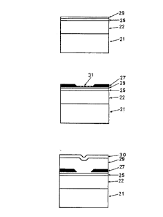
Figs. lA, lB and lC are section views showing fabrication
steps of a first embodiment of the invention;
Figs. 2A, 2B and 2C are section views showing fabrication
steps of a second embodiment of the invention;
Figs. 3A, 3B and 3C are section views showing fabrication
steps of a third embodiment of the invention;
Figs. 4A, 4B and 4C are section views showing fabrication
steps of fourth and fifth embodiments of the invention;
Figs. 5A, 5B and 5C are section views showing fabrication
steps of a sixth embodiment of the invention;
Fig. 6 is a view showing the configuration of an example
of an SCH-SAS LD;
Fig. 7 is a view showing the configuration of an example
of a PSCH-SAS LD;
Figs. 8A, 8B and 8C are views illustrating an example of
a conventional method of fabricating the SCH-SAS LD; and
Figs. 9A, 9B and 9C are views illustrating an example of
a conventional method of fabricating the PSCH-SAS LD.
DETAILED DESCRIPTION OF THE PREFERRED EMBODIMENT
Now referringto the drawings,preferredembodiments ofthe
invention are described below.
Figs. lA, lB and lC are section views showing fabrication
steps of a first embodiment of the invention. As shown in Fig.
- 19 -
CA 0224697~ 1998-09-14
lA, first, acladding layer 22 ofn-Al055Ga0.45As (thickness: 1.5
~m), a GaAs/Al0.45Ga0.55As quantum well active layer 25
(oscillation wavelength: 780 nm), and a part of a cladding layer
29 of p-Al0.55Ga0.4sAs (thickness: 0.20 ~m) are sequentially
crystal-grown on an n-GaAs substrate 21 by using an MOCVD or the
like.
In an AlGaAs material, as the Al composition is higher, the
bandgap tends to become wider. In the embodiment, the bandgap
of the cladding layers 22 and29 is wider than that of the quantum
well active layer 25.
Thesubstrateonwhichthecrystalgrowthhasbeenperformed
as described above is taken out from a crystal growth apparatus
and then loaded into an electron beam evaporation apparatus or
the like so that, as shown in Fig. lB, a mask 31 of, for example,
SiO2 iS formed on the whole surface at a thickness of 0.1 ~m.
Thereafter, the mask is removed away except a center portion
where a stripe-like window is to be formed, by using the
photolithography technique, thereby forming the mask 31 into a
stripe-like shape. Since the mask 31 is very thin, the
stripe-like mask can be accurately formed with high
reproducibility, even by the conventional photolithography
technique.
Next, the substrate on which the mask 31 is formed is
returned to the crystal growth apparatus, and a current blocking
layer 27 of n-GaAs (thickness: 0.80 ~m) is selectively grown
- 20 -
CA 0224697~ 1998-09-14
on the cl~ ng layer 29. As a result, as shown in Fig. lB, a
layer structure in which crystal growth is not performed in the
region where the mask 31 is formed is obtained.
Thereafter, the mask 31 is removed away by a hydrofluoric
acid aqueous solution or the like. As shown in Fig. lC, then,
the re~-ining part (thickness: 1.5 ~m) of the cladding layer
29 and a contact layer 30 of p-GaAs (thickness: 2.0 ~m) are
sequentially crystal-grown.
In this way, by using the technique in which the mask 31
is formed in the portion where the stripe-like window is to be
formed,thecurrentblockinglayer27isthenformedbyselective
growth, and the mask 31 is thereafter removed away, the
dimensions of the stripe-like window of the current blocking
layer 27 in the height and width directions can be accurately
controlled with high reproducibility while suppressing
maleffectsonthe layerssuch astheactivelayer25. As aresult
of this selective growth of the current blocking layer 27, a
self-aligned structure semiconductor laser which is excellent
in oscillation threshold and stability of the lateral mode can
be fabricated with a high yield.
The material of the mask 31 is not restricted to SiO2. Any
material such as SiN may be used as far as it can be selectively
grown.
Figs. 2A, 2B and 2C are section views showing fabrication
steps of a second embodiment of the invention. As shown in Fig.
- 21 -
CA 0224697~ 1998-09-14
2A, first, a claddlnglayer 22 ofn-Al0.4sGa0.ssAs (thickness: 1.5
~m), a GaAs/Al0.2oGao.aoAs quantum well active layer 25
(oscillation wavelength: 860 nm), and an optical guide layer 28
of p-Al0.30GaO.7oAs (thickness: 0.10 ~m) are sequentially
crystal-grown on an n-GaAs substrate 21 by using an MOCVD or the
like.
In an AlGaAs material, as the Al composition is higher, the
bandgap tends to become wider. In the embodiment, the bandgap
of the cladding layers 22 and 29 iswider than that of the quantum
well active layer 25.
Thesubstrateonwhichthecrystalgrowthhasbeenperformed
as described above is taken out from a crystal growth apparatus
and then loaded into an electron beam evaporation apparatus or
the like so that ,as shown in Fig. 2B, a mask 31 of, for example,
SiO2 iS formed on the whole surface at a thickness of 0.1 ~m.
Thereafter, the mask is removed away except a center portion
where a stripe-like window is to be formed, by using the
photolithography technique, thereby forming the mask 31 into a
stripe-like shape. Since the mask 31 is very thin, the
stripe-like mask can be accurately formed with high
reproducibility, even by the conventional photolithography
technique.
Next, the substrate on which the mask 31 is formed is
returned to the crystal growth apparatus, and a current blocking
layer 27 of n-GaAs (thickness: 0.80 ~m) is selectively grown
- 22 -
CA 0224697~ 1998-09-14
on the cl~tng layer 29. As a result, as shown in Fig. 2B, a
layer structure in which crystal growth is not performed in the
region where the mask 31 is formed is obtained.
Thereafter, the mask 31 is removed away by a hydrofluoric
acid aqueous solution or the like. As shown in Fig. 2C, then,
the cladding layer 29 (thickness: 1.5 ~m) and a contact layer
30Ofp-GaAs(thickness:2.0 ~m)aresequentiallycrystal-grown.
In this way, by using the technique in which the mask 31
is formed in the portion where the stripe-like window is to be
formed, thecurrentblockinglayer27 isthen formedbyselective
growth, and the mask 31 is thereafter removed away, the
dimensions of the stripe-like window of the current blocking
layer 27 in the height and width directions can be accurately
controlled with high reproducibility while suppressing
maleffects onthelayerssuchastheactivelayer25. As aresult
of this selective growth of the current blocking layer 27, a
self-aligned structure semiconductor laser which is excellent
ln oscillation threshold and stability of the lateral mode can
be fabricated with a high yield.
The material of the mask 31 is not restricted to SiO2. Any
material such as SiN may be used as far as it can be selectively
grown.
Figs. 3A, 3B and 3C are section views showing fabrication
steps of a third embodiment of the invention. As shown in Fig.
3A, first, acl~ ng layer 22 of n-Al024GaO.~6As (thickness: 1.1
- 23 -
CA 0224697~ 1998-09-14
~m),anopticalguidelayer230fn-Al0.20Ga080As(thickness:0.88
~m), an InO.20Ga080As/GaAs quantum well active layer 25
(oscillation wavelength: 980 nm), and a part of an optical guide
layer 28 ofp-Al0.20Ga0.80As(thickness:0.10 ~m) are sequentially
crystal-grown on an n-GaAs substrate 21 by using an MOCVD or the
like.
In an AlGaAs material, as the Al composition is higher, the
bandgap tends to become wider. In the embodiment, the bandgap
of the optical guide layers 23, 28 is wider than that of the
quantum well active layer 25, and the bandgap of the cladding
layer 22 and a later-mentioned cladding layer 29 is wider than
that of the optical guide layers 23, 28.
In this embodiment, the optical guide layer 23 is formed
tobethickerthanthatintheconventionalSCH-SASsemiconductor
laser. Furthermore, the bandgap of the optical guide layer 23
is set to be sufficiently wider than that of the quantum well
active layer 25, therebypreventingthecarrier fromoverflowing
to the optical guide layers 23, 28 from the active layer 25.
Thesubstrateonwhichthecrystalgrowthhasbeenperformed
as described above is taken out from a crystal growth apparatus
and then loaded into an electron beam evaporation apparatus or
the like so that ,as shown in Fig. 3B, a mask 31 of, for example,
SiO2 is formed on the whole surface at a thickness of 0.1 ~m.
Thereafter, the mask is removed away except a center portion
where a stripe-like window is to be formed, by using the
- 24 -
CA 0224697~ 1998-09-14
photolithography technique, thereby forming the mask 31 into a
stripe-like shape. Since the mask 31 is very thin, the
stripe-like mask can be accurately formed with high
reproducibility, even by the conventional photolithography
technique.
Next, the substrate on which the mask 31 is formed is
returned to the crystal growth apparatus, and a current blocking
layer 27 of n-Al0.33GaO.67As (thickness: 0.1 ~m) is selectively
grown on the optical guide layer 28. As a result, as shown in
Fig. 3B, a layer structure in which crystal growth is not
performed in the region where the mask 31 is formed is obtained.
Thereafter, the mask 31 is removed away by a hydrofluoric
acid aqueous solution or the like. As shown in Fig. 3C, then,
the re~in~ng part (thickness: 0.78 ~m) of the optical guide
layer 28 is crystal-grown, and further the cladding layer 29
of p-Al0.24GaO.~6As (thickness: 1.1 ~m) and a contact layer 30 of
p-GaAs (thickness:2.0 ~m) aresequentiallycrystal-grown. The
thickness of the optical guide layer at the stripe-like window
is preferably 0.2 ~m or more which is thicker than that of the
conventional SCH-SAS LD.
In this way, by using the technique in which the mask 31
is formed in the portion where the stripe-like window is to be
formed, thecurrentblockinglayer27 isthenformedbyselective
growth, and the mask 31 is thereafter removed away, the
dimensions of the stripe-like window of the current blocking
- 25 -
CA 0224697~ 1998-09-14
layer 27 in the height and width directions can be accurately
controlled with high reproducibility while suppressing
maleffects on the other layers such as the active layer 25. As
a result of this selective growth of the current blocking layer
27, an SCH-SAS LD which is excellent in oscillation threshold
and stability of the lateral mode can be fabricated with a high
yield.
The material of the mask 31 is not restricted to SiO2. Any
material such as SiN may be used as far as it can be selectively
grown.
Figs. 4A, 4B and 4C are section views showing fabrication
steps of a fourth embodiment of the invention. As shown in Fig.
4A, first, acladding layer 22 of n-Al0.24Ga0.~6As (thickness: 1.1
~m),anopticalguidelayer230fn-Al0.20Ga0.80As(thickness:0.88
~m),acarrierblockinglayer240fann-Al0.50Ga0.50As(thickness:
0.025 ~m), a GaAs/Al0.20Ga0.8oAs quantum well active layer 25
(oscillation wavelength: 860 nm), a carrier blocking layer 26
of p-Al0.50Ga0.5oAs (thickness: 0.025 ~m) and a part of an optical
guide layer 28 of p-Al0.20Ga0.8oAs (thickness: 0.10 ~m) are
sequentially crystal-grown on an n-GaAs substrate 21 by using
an MOCVD or the like.
In an AlGaAs material, as the Al composition is higher, the
bandgap tends to become wider. In the embodiment, the bandgap
of the optical guide layers 23, 28 is wider than that of the
quantum well active layer 25, and the bandgaps of the cladding
- 26 -
CA 0224697~ 1998-09-14
layers 22, 29 and the carrier blocking layers 24, 26 are wider
than that of the optical guide layers 23, 28.
Thesubstrateonwhichthecrystalgrowthhasbeenperformed
as described above is taken out from a crystal growth apparatus
and then loaded into an electron beam evaporation apparatus or
the like so that ,as shown in Fig. 4B, a mask 31 of, for example,
SiO2 iS formed on the whole surface at a thickness of 0.1 ~lm.
Thereafter, the mask is removed away except a center portion
where a stripe-like window is to be formed, by using the
photolithography technique, thereby forming the mask 31 into a
stripe-like shape. Since the mask 31 is very thin, the
stripe-like mask can be accurately formed with high
reproducibility, even by the conventional photolithography
technique.
Next, the substrate on which the mask 31 is formed is
returnedto the crystal growth apparatus, and a current blocking
layer 27 of n-Al0.33GaO.6~As (thickness: 0.1 ~m) is selectively
grown on the optical guide layer 28. As a result, as shown in
Fig. 4B, a layer structure in whlch crystal growth is not
performed in the region where the mask 31 is formed is obtained.
Thereafter, the mask 31 is removed away by a hydrofluoric
acid aqueous solution or the like. As shown in Fig. 4C, then,
the remaining part (thickness: 0.78 ~m) of the optical guide
layer 28 is crystal-grown, and further the cladding layer 29 of
p-Al0.24GaO.76As (thickness: 1.1 ~m) and a contact layer 30 of
CA 0224697~ 1998-09-14
p-GaAs (thickness: 2.0 ~m) are sequentially crystal-grown.
In this way, by using the technique in which the mask 31
is formed in the portion where the stripe-like window is to be
formed,the currentblockinglayer27isthen formedbyselective
growth, and the mask 31 is thereafter removed away, the
~imensions of the stripe-like window of the current blocking
layer 27 in the height and width directions can be accurately
controlled with high reproducibility while suppressing
maleffects on the other layers such as the active layer 25 or
the carrier blocking layer 26. As a result of this selective
growth of the current blocking layer 27, an SCH-SAS LD which is
excellent in oscillation threshold and stability of the lateral
mode can be fabricated with a high yield.
The material of the mask 31 is not restricted to SiO2. Any
material such as SiN may be used as far as it can be selectively
grown.
Fig. 5A, 5B and 5C are section views showing fabrication
steps of a fifth embodiment of the invention. In the present
embodiment, the explanation will made also by referring Figs.
4A, 4B and 4C. As shown in Fig. 4A, first, a cladding layer 22
of n-Al0.l~GaO.83As (thickness: 1.7 ~m), an optical guide layer
23 of n-GaAs (thickness: 0.55 ~m), a carrier blocking layer 24
of n-Al0.30GaO.7oAs (thickness: 0.030 ~m), an InO.2GaO.8As/GaAs
quantum well active layer 25 (oscillation wavelength: 980 nm),
a carrier blocking layer 26 of p-Al0.30GaO.7oAs (thickness: 0.030
CA 0224697~ 1998-09-14
~m) and apart of an optical gulde layer 28 of p-GaAs (thickness:
0.10 ~m) are sequentially crystal-grown on an n-GaAs substrate
21 by using an MOCVD or the like.
In an AlGaAs material, as the Al composition is higher, the
bandgap tends to become wider. In the embodiment, the bandgap
of the optical guide layers 23, 28 is wider than that of the
quantum well active layer 25, and the bandgaps of the cladding
layers 22, 29 and the carrier blocking layers 24, 26 are wider
than that of the optical guide layers 23, 28.
Thesubstrateonwhichthecrystalgrowthhasbeenperformed
as described above is taken out from a crystal growth apparatus
and then loaded into an electron beam evaporation apparatus or
the like so that, as shown in Fig. 4B, a mask 31 of, for example,
SiO2 iS formed on the whole surface at a thickness of 0.1 llm.
Thereafter, the mask is removed away except a center portion
where a stripe-like window is to be formed, by using the
photolithography technique, thereby forming the mask 31 into a
stripe-like shape. Since the mask 31 is very thin, the
stripe-like mask can be accurately formed with high
reproducibility, even by the conventional photolithography
technique.
Next, the substrate on which the mask 31 is formed is
returned to the crystal growth apparatus, and a current blocking
layer 27 of n-Al0.08Ga0.92As (thickness: 0.15 ~m) is selectively
grown on the optical guide layer 28. As a result, as shown in
- 29 -
CA 0224697~ 1998-09-14
Fig. 4B, a layer structure in which crystal growth is not
performed in the region where the mask 31 is formed is obtained.
Thereafter, the mask 31 is removed away by a hydrofluoric
acid aqueous solution or the like. As shown in Fig. 4C, then,
the remaining part (thickness: 0.45 ~m) of the optical guide
layer 28 is crystal-grown, and further the cladding layer 29 o,f
p-Al0l7GaO.83As (thickness: 1.7 ~m) and a contact layer 30 of
p-GaAs (thickness: 2.0 ~m) are sequentially crystal-grown.
In this way, by using the technique in which the mask 31
is formed in the portion where the stripe-like window is to be
formed,the currentblocking layer27 isthen formedby selective
growth, and the mask 31 is thereafter removed away, the
dimensions of the stripe-like window of the current blocking
layer 27 in the height and width directions can be accurately
controlled with high reproducibility while suppressing
maleffects on the other layers such as the active layer 25 or
the carrier blocking layer 26. As a result of this selective
growth of the current blocking layer 27, an SCH-SAS LD which is
excellent in oscillation threshold and stability of the lateral
mode can be fabricated with a high yield. In addition, owing
to the GaAs guide layers, lt is possible to avoid the effect of
the deterioration due to the oxidation. As a result, a
semiconductor laser of high reliability in which a barrier is
not formed can be fabricated and realized.
The material of the mask 31 is not restricted to SiO2. Any
- 30 -
CA 0224697~ 1998-09-14
material such as SiN may be used as far as it can be selectively
grown.
Figs. 5A, 5B and 5C are section views showing fabrication
steps of a sixth embodiment of the invention. As shown in Fig.
5A, first, acladdinglayer 22 of n-Al024Ga0.76As (thickness: 1.1
~m),anopticalguidelayer230fn-Al0.20Ga0.80As(thickness:0.88
~m), a carrier blocking layer 24 of n-Al0.50Ga0~5oAs (thickness:
0.025 ~m), a GaAs/Al0.20Ga0.8oAs quantum well active layer 25
(oscillation wavelength: 860 nm), a carrier blocking layer 26
of p-Al0.50Ga0.5oAs (thickness: 0.025 ~m), an optical guide layer
280fp-Al0.20Ga0.80As(thickness:0.10 ~m),andaprotectivelayer
32 of p-In0.49Ga0.51P (thickness: 0.02 ~m) are sequentially
crystal-grown on an n-GaAs substrate 21 by using an MOCVD or the
like.
In an AlGaAs material, as the Al composition is higher, the
bandgap tends to become wider. In the embodiment, the bandgap
of the optical guide layers 23, 28 is wider than that of the
quantum well active layer 25, and the bandgaps of the cladding
layers 22, 29 and the carrier blocking layers 24, 26 are wider
than that of the optical guide layers 23, 28.
Since the protective layer 32 is formed of a material free
of aluminum, it is possible to suppress the deterioration due
to the oxidation.
Thesubstrateonwhichthecrystalgrowthhasbeenperformed
as described above is taken out from a crystal growth apparatus
- 31 -
CA 0224697~ 1998-09-14
and then loaded into an electron beam evaporation apparatus or
the like so that, as shown in Fig. 5B, a mask 31 of, for example,
SiO2 is formed on the whole surface at a thickness of 0.1 ~m.
Thereafter, the mask is removed away except a center portion
where a stripe-like window is to be formed, by using the
photolithography technique, thereby forming the mask 31 into a
stripe-like shape. Since the mask 31 is very thin, the
stripe-like mask can be accurately formed with high
reproducibility, even by the conventional photolithography
technique.
Next, the substrate on which the mask 31 is formed is
returned to the crystal growth apparatus, and a current blocking
layer 27 of n-Al033GaO.67As (thickness: 0.1 ~m) is selectively
grown on the optical guide layer 28. As a result, as shown in
Fig. 5B, a layer structure in which crystal growth is not
performed in the region where the mask 31 is formed is obtained.
Thereafter, the mask 31 is removed away by a hydrofluoric
acid aqueous solution or the like. As shown in Fig. 5C, then,
the remaining part (thickness: 0.78 ~m) of the optical guide
layer 28 is crystal-grown, and further the cladding layer 29 of
p-Al0.24GaO.76As (thickness: 1.1 ~m) and a contact layer 30 of
p-GaAs (thickness: 2.0 ~m) are sequentially crystal-grown.
In this way, by using the technique in which the mask 31
is formed in the portion where the stripe-like window is to be
formed,the currentblocking layer27 isthen formedbyselective
- 32 -
CA 0224697~ 1998-09-14
growth, and the mask 31 is thereafter removed away, the
dimensions of the stripe-like window of the current blocking
layer 27 in the height and width directions can be accurately
controlled with high reproducibility while suppressing
maleffects on the active layer 25 or the carrier blocking layer
26. As a result of this selectivegrowth of the current blocking
layer 27, an SCH-SAS LD which is excellent in oscillation
threshold and stability of the lateral mode can be fabricated
with a high yield.
In addition, by providing the protective layer 32 formed
of InO.49GaO.5lP, it is possible to avoid the effect of the
deteriorationduetotheoxidation. Asaresult,asemiconductor
laser of high reliability in which a barrier is not formed can
be fabricated and realized.
The material of the mask 31 is not restricted to SiO2. Any
material such as SiN may be used as far as it can be selectively
grown.
The invention may be embodied in other specific forms
without departing from the spirit or essential characteristics
thereof. Thepresentembodimentsarethereforetobeconsidered
in all respects as illustrative and not restrictive, the scope
of the invention being indicated by the appended claims rather
than by the foregoing description and all changes which come
within the meaning and the range of equivalency of the claims
are therefore intended to be embraced therein.