Note: Descriptions are shown in the official language in which they were submitted.
CA 02247548 1999-09-30
A HIGH-SPEED ASYNCHRON008 DECOMPREBSION CIRCOIT
FOR VARIABLE-LENGTH-CODED DATA
BACKGROUND OF THE INVENTION
This invention relates to an asynchronous decoder circuit. More
specifically, this invention relates to an asynchronous decoder circuit that
operates on
data coded using a variable-length coding technique, such as Huffman coding.
Huffman coding is a lossless coding technique that replaces fixed-length
symbols with variable-length codes. Huffman codes are entropy-based, meaning
that
short codes are assigned to frequently occurring symbols and longer codes are
assigned to
less frequently occurring symbols. In addition, Huffman codes are prefix
codes, meaning
that each code has the property that appending additional bits to the end of
the code never
produces another valid code. Advantageously, Huffman coding has been used for
the
compression of data.
In applications utilizing Huffman-coded data, the size and speed of a
Huffman decoder are important. For example, small and fast Huffman decoders
are
necessary in compressed-code systems and MPEG-2 video systems. A compressed-
code
system is a microprocessor or microcontroller-based system in which
instructions are
NY02:167383.1 - 2 -
CA 02247548 1999-09-30
stored in compressed form in memory, then are decompressed when brought into a
cache.
As a result, a significant reduction in instruction memory size may be
obtained. The
design of a decompression circuit for these systems is highly constrained. In
particular,
the circuit must be very fast (since it is on the critical path between the
processor and
memory) and must also be very small (otherwise the savings in instruction
memory will
be lost to the area increase due to the decompression circuit). MPEG-2 is an
international
image coding standard promulgated by the International Standardization
Organization
(ISO), which requires data to be decoded at a rate of 100 Mbits/sec or greater
to maintain
a sufficient quality of audio and video output.
To date, there have been two commonly used approaches to the design of
Huffman decoders, which have been commonly referred to as the constant-input-
rate
approach and the constant-output-rate approach. Both of these approaches are
synchronous-i.e., the decoders are synchronized to an external system clock.
In the constant-input-rate approach, the input data stream is processed at a
rate of one bit per clock cycle by traversing a Huffman code tree through the
use of a
finite state machine. To achieve a high performance using this type of design
requires a
very fast clock, introducing many very difficult high-speed circuit problems.
In fact, it is
unlikely that a state machine of adequate complexity can be designed to run at
the speeds
required by the constant-input-rate approach on a silicon wafer produced by
certain
semiconductor processes, such as those using 0.8,u or thicker CMOS wafers. To
avoid
NY02:167383.1 ' 3
CA 02247548 1999-09-30
the problems caused by the use of very high-speed clocks, multiple state
transitions may
be combined into a single cycle. As multiple state transitions are combined,
however, the
complexity and circuit area of the decoder increase approximately
exponentially with
respect to the increased performance per clock cycle.
In the constant-output-rate approach, a portion of the input data stream, at
least as long as the longest input symbol, is translated into an output symbol
on each
clock cycle. One disadvantage to this approach is that it requires more
complex shifting
and symbol detection circuitry than the constant-input-rate approach.
Furthermore, the
input data buffer and shifting circuitry must be wide enough to store and
shift the longest
of the input symbols, which is inefficient since the most frequently occurring
input
symbols will be shorter than the longest input symbol. Another significant
disadvantage
of the constant-output-rate approach is that the length of the critical path
is dominated by
the time to detect and decode the longest input symbol. Thus, the vast
majority of cycles
are limited by a very infrequent worst-case path.
I 5 In sum, each of the two commonly-used approaches to the design of
Huffman decoders requires a compromise between the performance and the
complexity
(circuit area) of the implementations. Accordingly, there exists a need for an
improved
Huffman decoder design that provides higher performance per circuit area than
is
possible with existing circuit designs.
NY02:167383.1 - 4 -
CA 02247548 1999-09-30
SUMMARY OF THE INVENTION
The present invention solves the foregoing problems by employing an
innovative asynchronous design, which produces a decoder that is significantly
smaller
than comparable synchronous decoders, and yet has a higher throughput rate
than these
decoders after normalizing for voltage and process differences between the
decoders.
According to the present invention, there is provided a decoder circuit,
which includes a logic circuit for decoding variable-length coded data and a
timing
circuit. The logic circuit includes a plurality of computational logic stages,
each of the
computational logic stages having a synchronization signal input and a
completion signal
output. Each completion signal output indicates the completion of the
computation
performed by a computational logic stage. The timing circuit includes a
plurality of
completion signal inputs, which are coupled to the completion signal outputs
of the
computational logic stages, and a synchronization signal output, which is
coupled to the
synchronization signal inputs of the computational logic stages. The
synchronization
signal output of the timing circuit is not a periodic signal with a fixed
cycle period.
Instead, the synchronization signal is an asynchronous output determined as a
function of
the completion signal inputs.
In a preferred embodiment of the present invention, the decoder operates
on data that has been coded according to a variable-length coding technique in
which
coded data words are classified according to their word length and the
occurrence of
NY02:16T83.1 - 5 -
CA 02247548 1999-09-30
common bits therein. The common bits are unique relative to at least a subset
of the
classes of the coded data words. In such an embodiment, the logic circuit of
the decoder
includes: an alignment circuit for shifting an input data word by an amount
responsive to
a control input and for outputting the shifted data word; a match logic
circuit coupled to
the output of the alignment circuit for decoding the class of a coded data
word included in
the shifted data word; a decode logic circuit coupled to the output of the
alignment circuit
for decoding the coded data word included in the shifted data word; a length
logic circuit
coupled to the output of the match logic circuit for determining the length of
the coded
data word included in the shifted data word; an offset register having a
register data input
and a register data output, the register data output coupled to the control
input of the
alignment circuit; and an adder circuit for adding first and second adder
inputs, the first
adder input coupled to the output of the length logic circuit and the second
adder input
coupled to the register data output, the output of the adder circuit coupled
to the register
data input.
The decoder circuit is preferably designed such that the alignment circuit,
the match logic circuit, and the adder circuit comprise a computational logic
stage, and
the alignment circuit, the match logic circuit, and the decode logic circuit
comprise
another computational logic stage.
The adder circuit may include a carry output indicative of a carry resulting
from the addition of the first and second adder inputs, and the logic circuit
may further
NY02:167383.1 - 6
CA 02247548 1999-09-30
include an input buffer having a plurality of registers. The registers may be
coupled
together in series, and the data output of one or more of the registers may be
coupled to
the data input of the alignment circuit.
The logic circuit may further include a shift sequence circuit coupled to
the carry output of the adder circuit and to the clock inputs of the input
registers for
shifting the input registers responsive to the carry output of the adder
circuit.
The decoder circuit may further include input and output handshaking
circuits for implementing an asynchronous handshake between the decoder
circuit and
external circuits coupled to the decoder circuit.
NY02:167383.1 ' 7 -
CA 02247548 1999-09-30
BRIEF DESCRIPTION OF THE DRAWINGS
Exemplary embodiments of the present invention will now be described in
detail with reference in the accompanying drawings in which:
Fig. 1 A is a functional block diagram of a decoder according to a preferred
embodiment of the present invention;
Fig. 1 B is a functional block diagram of a decoder according to another
preferred embodiment of the present invention;
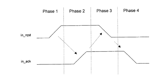
Fig. 2 is an exemplary timing diagram for an asynchronous, four-phase
handshaking protocol that may be used with a decoder according to the
embodiment of
Fig. 1 B;
Fig. 3 is a functional block diagram of an input buffer of a decoder
according to the embodiment of Fig. 1 B;
Fig. 4 is a functional block diagram of an input buffer according to the
embodiment of Fig. 3;
Fig. 5 is a schematic diagram of a latch of an input buffer according to the
embodiment of Fig. 4;
Fig. 6 is a schematic diagram of a latch of an input buffer according to the
embodiment of Fig. 4;
Fig. 7 is a schematic diagram of a latch of an input buffer according to the
embodiment of Fig. 4;
NY02:167383.1 - 8 -
CA 02247548 1999-09-30
Fig. 8 is a schematic diagram of a latch of an input buffer according to the
embodiment of Fig. 4;
Fig. 9 is a schematic diagram of a latch of an input buffer according to the
embodiment of Fig. 4;
Fig. 10 is a schematic diagram of a reload sequencer circuit of a decoder
according to the embodiment of Fig. 1 B;
Fig. 11 is a signal transition diagram for the reload sequencer circuit of
Fig. 10;
Fig. 12 is a functional block diagram of an alignment circuit of a decoder
according to the embodiment of Fig. 1B;
Fig. 13 is a partial functional block diagram of an alignment circuit
according to the embodiment of Fig. 12;
Fig. 14 is a schematic diagram of a buffer of an alignment circuit
according to the embodiment of Fig. 13;
Fig. 15 is a schematic diagram of a buffer of an alignment circuit
according to the embodiment of Fig. 13;
Fig. 16 is a functional block diagram of a preferred embodiment of a
match logic circuit of a decoder according to the embodiment of Fig. 1 B;
Fig. 17 is a functional block diagram of an inverter circuit for the outputs
of a match logic circuit according to the embodiment of Fig. 16;
NY02:167383.1 - 9 -
CA 02247548 1999-09-30
Fig. 18 is a schematic diagram of a decoder of a match logic circuit
according to the embodiment of Fig. 16;
Fig. 19 is a partial functional block diagram of a symbol decoder ROM of
a decoder according to the embodiment of Fig. 1 B;
Fig. 20 is a functional block diagram of an adder circuit of a decoder
according to the embodiment of Fig. 1 B;
Fig. 21 is a schematic diagram of a "bit 0" circuit of an adder circuit
according to the embodiment of Fig. 20;
Fig. 22 is a schematic diagram of a "bit 1" circuit of an adder circuit
according to the embodiment of Fig. 20;
Fig. 23 is a schematic diagram of a "shift" circuit of an adder circuit
according to the embodiment of Fig. 20;
Fig. 24 is a functional block diagram of a preferred embodiment of an
offset register of a decoder according to the embodiment of Fig. 1B;
1 ~ Fig. 25 is a schematic diagram of a preferred embodiment of an RS latch
of an offset register according to the embodiment of Fig. 24;
Fig. 26 is a functional block diagram of a preferred embodiment of a shift
sequencer circuit of a decoder according to the embodiment of Fig. 1B;
Fig. 27 is a schematic diagram of a preferred embodiment of a shift
sequencer circuit according to the embodiment of Fig. 26;
NY02:167383.1 - 1 ~ -
CA 02247548 1999-09-30
Fig. 28 is a functional block diagram of a preferred embodiment of a
symbol decode circuit of a decoder according to the embodiment of Fig. 1B;
Fig. 29 is a functional block diagram of a preferred embodiment of a
decode logic stage of a symbol decode circuit according to the embodiment of
Fig. 28;
Fig. 30 is a partial block diagram of a decoder group of the decode logic
stage of Fig. 29;
Fig. 31 is a schematic diagram of a preferred embodiment of a decoder of
a symbol decode circuit according to the embodiment of Fig. 30;
Fig. 32A is a preferred embodiment of a merge circuit of a decoder
according to the embodiment of Fig. 1 B;
Fig. 32B is a preferred embodiment of a buffer of the merge circuit of Fig.
32A;
Fig. 32C is a preferred embodiment of a buffer of the merge circuit of Fig.
32A;
Fig. 33 is a preferred embodiment of an output buffer of a decoder
according to a the embodiment of Fig. 1 B;
Fig. 34 is a functional block diagram of a preferred embodiment of an
output handshake circuit of a decoder according to the embodiment of Fig. 1 B;
Fig. 35 is a functional block diagram of a preferred embodiment of a
timing control circuit of a decoder according to the embodiment of Fig. 1 B;
NY02:167383.1 - 1 1 -
CA 02247548 1999-09-30
Fig. 36 is a preferred embodiment of a layout of a decoder according to the
embodiment of Fig. 1 B;
Fig. 37 is an exemplary timing diagram of a decoder according to the
embodiment of Fig. 1 B; and
Fig. 38 is a block diagram of a compressed-code microprocessor system
according to a preferred embodiment of the present invention.
Throughout the figures of the drawings, the same reference numerals or
characters are used to denote like components or features of the invention.
NY02:167383.1 - 12 -
CA 02247548 1999-09-30
DETAILED DESCRIPTION
Fig. 1 A is a functional block diagram of a decoder according to the present
invention. The decoder 10 includes a logic circuit 20 coupled to a timing
control circuit
30. The logic circuit 20 decodes data words encoded using a variable-length
coding
technique, such as Huffman coding. The logic circuit 20 includes a plurality
of functional
blocks (represented in Fig. 1 A as functional blocks 1 to N). The functional
blocks have
completion signal outputs, done_l, done 2, . . . done N, which indicate the
completion
of the computation performed by the functional blocks.
The timing circuit 30 generates a synchronization signal main clk for
synchronizing the operation of the functional blocks of Fig. lA.
Advantageously, unlike
prior synchronous designs, the synchronization signal main clk is not derived
from an
external or internal periodic clock signal. Instead, the transitions of the
synchronization
signal main clk are based on the completion signals from one or more of the
functional
blocks. Thus, although the decoder of Fig. lA decodes one code word per cycle
of the
1 ~ synchronization signal main clk, the length of that cycle varies depending
on the time it
takes to decode a particular code word.
Fig. 1 B is a functional block diagram of a decoder according to a preferred
embodiment of the present invention. The decoder of Fig. 1 B includes an input
buffer
100, which receives and stores input data that has been coded using a variable-
length
coding technique, such as Huffman coding. Coded data is input into the input
buffer 100
NY02:167383.1 - 13 -
CA 02247548 1999-09-30
in fixed-length words (for example, 32-bit words).
Input data is input into the input buffer 100 under the control of a reload
sequencer circuit 150. The reload sequencer circuit 150 preferably implements
an
asynchronous handshake with the circuit providing the input data, such as the
asynchronous, four-phase handshake shown in Fig. 2. As shown in Fig. 2, in the
first
phase of the handshake, the handshake is initiated by the assertion (the low-
to-high
transition) of the request signal in rqst by the circuit providing the input
data, which
indicates that the input data is valid. In the second phase of the handshake,
after the
request signal in rqst is asserted, the input data is read into the input
buffer 100. Once
the input data has been read into the input buffer, the acknowledge signal in
ack is
asserted (by low-to-high transition) by the reload sequencer circuit 150. In
the third
phase, in response to the assertion of the acknowledge signal in ack, the
request signal
in rqst is released (high-to-low transition), indicating the input data is no
longer valid.
Finally, in the fourth phase, after the request signal in rqst is released,
the acknowledge
signal in ack is also released after the input buffer 100 is ready to receive
more data.
Returning to Fig. 1 B, because the coded data in the input buffer 100
contains variable-length code words, the beginning of a code word may not
always be
aligned with the first bit of the input buffer. (In fact, it usually will not
be.) Accordingly,
the unaligned data from the input buffer 100 is coupled to an alignment
circuit 200,
which is capable of shifting the input data by the number of bits indicated by
an offset
NY02:167383.1 - 14 -
CA 02247548 1999-09-30
register 900.
The decoder of Fig. 1 B preferably operates on data that is coded according
to a variable-length coding technique in which coded data words may be
classified
according to their word length and the occurrence of common bits therein. The
common
bits are unique relative to at least a subset of the classes of the coded data
words. When
data is coded in this way, the decoding process is preferably performed in two
stages.
The first stage of the decoding process is performed by a match logic circuit
300, and the
second stage of the decoding process is performed by a symbol decode circuit
600.
The aligned data from the alignment circuit 200 is coupled to both the
match logic circuit 300 and the symbol decode circuit 600. By examining the
aligned
data from the alignment circuit 200 for the common bits of each class, the
match logic
circuit 300 determines the class of a code word. Using the code word class
from the
match logic circuit 300 and the enumerating bits of the aligned data from the
alignment
circuit 200 (as will be explained below), the symbol decode circuit 600
determines the
symbol corresponding to a code word. This symbol is transmitted to an output
buffer
700, which stores one or more symbols for transmission in an appropriate-
length word.
For example, if the symbols are eight bits in length, and the output word is
32 bits in
length, the output buffer 700 will store four symbols before transmitting an
output word.
The output buffer 700 communicates with an output handshake circuit
750, which implements an asynchronous handshake with the circuit receiving the
output
NY02:167383.1 - 15 -
CA 02247548 1999-09-30
data. The output handshake may be the same asynchronous, four-phase handshake
discussed previously with regard to the reload sequences circuit 150.
At the same time as the symbol decode circuit 600 performs its
computation, a length read-only memory (ROM) 400 concurrently determines the
length
of a code word associated with the code word class provided by the match logic
circuit
300. An adder circuit 500 then sums the code word length from the length ROM
400 and
the offset value in the offset register 900. The sum produced by the adder
circuit 500
determines a new offset value, which is stored in the offset register 900 and
which
indicates the offset of the next code word contained in the input buffer 100.
Preferably, to reduce the hardware of the alignment circuit 200, the input
buffer 100 includes a plurality of registers connected together sequentially
through which
the input data may be shifted. These registers are preferably controlled by a
shift
sequences circuit 800. The shift sequences circuit 800 is coupled to the input
buffer 100,
the adder circuit 500, and the reload sequences circuit 150.
The decoder of Fig. 1B also includes a timing control circuit 1000, which
generates the synchronization signal main clk for synchronizing the operation
of the
functional blocks of Fig. 1 B. As discussed previously, the synchronization
signal
main clk is not derived from an external or internal periodic clock signal.
Instead, the
transitions of the synchronization signal main clk are based on completion
signals from
one or more of the functional blocks of Fig. 1 B. For example, as shown in
Fig. 1 B, the
NY02:167383.1 - 16 -
CA 02247548 1999-09-30
transitions of the synchronization signal main clk may be based on the
completion
signals add done, code done, shift done, and out done from the adder circuit
500, the
symbol decode circuit 600, the shift sequencer circuit 800, and the output
handshake
circuit 750, respectively. Advantageously, the length of a decode cycle is not
fixed, but
instead varies depending on the time it takes to decode a particular code
word.
Preferably, for improved efficiency, some of the functional blocks of Fig.
1 B may be implemented with dynamic (or precharged) domino logic. When the
functional blocks are implemented in this way, the operation of the decoder
may be
divided into two stages: an evaluation stage (during which the dynamic domino
logic
blocks evaluate their inputs) and a precharge stage (during which the dynamic
domino
logic blocks precharge). These two stages are advantageously controlled by the
state of
the synchronization signal main clk. For example, the evaluation stage may be
associated with the logic low cycle of the synchronization signal main clk,
and the
precharge stage may be associated with the logic high cycle of the
synchronization signal
main clk.
In a preferred embodiment of the present invention, the alignment circuit
200, match logic circuit 300, length ROM 400, adder 500, and symbol decode
circuit 600
are implemented in dynamic domino logic. Therefore, during the evaluation
stage these
functional blocks evaluate their inputs, and during the precharge stage these
functional
blocks precharge. Concurrently, while these functional blocks precharge, other
blocks
NY02:167383.1 - 1 7 -
CA 02247548 1999-09-30
may perform operations. For example, it is preferred that the shift sequencer
circuit 800
performs any necessary shifting of the registers of the input buffer 100
during the
precharge stage. The concurrent precharging of the dynamic domino logic blocks
and the
operation of other functional blocks enhances the performance of the decoder
of Fig. 1 B.
S For the purpose of illustrating the preferred two-stage decoding process of
the present invention, Table 1 shows an example of Huffman coding for the MIPS
processor instruction set. The codes used are based on measurements of the
frequency of
instructions from a sample set of programs for the MIPS architecture. The
Huffman
codes shown in Table 1 range in length from two bits to fourteen bits for each
instruction.
The length of each Huffman code in Table 1 is precisely determined by the
frequency distribution of the instructions for the MIPS architecture.
Nonetheless, the
actual bit encoding for each instruction is flexible, as long as the prefix
property and the
code length requirements of Huffman codes are maintained. The preferred
approach,
therefore, is to select code words of a given length such that those code
words contain as
many common bits as possible, which are unique to that group of code words. To
simplify the encoding process, the common bits need not be unique to all
classes.
Instead, an order of decoding may be assigned to the classes and the common
bits for a
class may be unique relative to the subset of classes occurring later in the
decoding order.
For example, note that all of the five-bit long Huffman codes shown in
Table 1 contain the string "010" as the initial three bits, while no other
code words
NY02:167383.1 - 1 g -
CA 02247548 1999-09-30
contain those values in those positions. This allows use of that substring in
that position
to define a class of 5-bit code words and allows use of the remaining bits to
enumerate
the members of that class. In many cases, the coding can be structured such
that only a
small number of bits are required to be tested in order to determine the
length of the
Huffman code.
Overall, for the coding shown in Table 1, the 256 different code words are
grouped into 3I distinct classes. This grouping of classes is shown in Table
2, along with
the common bit patterns for each class and the enumerating bits used to
distinguish the
class members. The decoding process begins at the top of the table with class
0 and
proceeds downward, class by class, until a match is found. In Table 2, a dash
("-")
represents a "don't care" and a period represents an enumerating bit.
NY02:167383.1 - I9 -
CA 02247548 1999-09-30
Table 1: Example of Huffman Coding for MIPS Architecture
00 00 2c1011100186110111000b61110111110fd 11111001010fa 111111100000
8f 01000 b01011101043110111001fe11101(11117e 11111001011f5 111111100001
24 OIOOI 0910111011b9110111010e2111100000065 1111100110056 111111100010
OI 01010 f8101111008a110111011e6111100000167 IIII1001101d2 111111100011
10 01011 e71011)1016c110111100ef1111000010t7 11111001110cd II1111100100
46 011000 a81011111032110111101d4111100001171 11111001111f6 111111100101
25 011001 ae10111111a9110111110ce1(110001003a 11111010000ed 111111100110
80 011010 8811000000Ob1101111117f11110001019e 11111010001~e 111111100111
08 011011 90110000014c1110000004611110001107b 1111101001077 111111101000
03 011100 e411000010as1110000014e11110001116b 11111010011f1 111111101001
21 011101 5011000011131110000103911110010006a 1111101010097 111111101010
Oc 011110 2a11000100641110000112f1111001001c3 11111010101c9 111111101011
04 011111 4411000101Od111000100do1111001010lb 111110101107d 111111101100
20 100000 bd110001106811100010145111100101166 1111101011155 111111101101
ff 100001 06110001112211100011051111100110035 11111011000ca 111111101110
02 100010 a5110010002b1110001116311110011014d 11111011001e9 111111101111
of 100011 bf11001001a711100100062111100111079 1111101101095 111111110000
c0 1001000 lc11001010a31110010019c1111001111le 111110110119b 111111110001
8c 1001001 8d1100101189111001010cf11110100003e 111110111009f 111111110010
8e 1001010 3811001100fc1110010114f1111010001be 11111011101tb 111111110011
84 1001011 1111001101ad111001100f4111101001047 1111101111069 111111110100
82 1001100 2611001110c8111001101521111010011el 1111101111153 111111110101
e0 1001101 a411001111231110011109l1111010100if 11111100000eb 111111110110
28 1001110 ac1101000031111001111991111010101b7 1111110000196 111111110111
c4 1001111 a01101000187111010000Sc111101011049 11111100010d7 1111111110000
30 1010000 OS1101001081111010001c5111101011133 11111100011da 1111111110001
18 1010001 6011010011IS1110100101711110110006f 11111100100d3 1111111110010
c7 1010010 2e11010100058111010011c1111101100136 11111100101bb 1111111110011
14 1010011 ab110101001981110101007c1111011010e5 11111100110d5 1111111110100
40 1010100 63110101010Oa11101010161111101101193 111111001119d 1111111110101
27 1010101 29110101011Of111010110651111011100f9 11111101000Sd II11111110110
3c 1010110 9211010110083111010111b21111011101Ia 111111010019a II11111110111
12 1010111086110101101a2111011000e81111011110ee 1111110101075 III1111111000
48 10101111d8110101110a611101100174111101111176 111111010110Sf 1111111111001
42 10110000bl110101111Oe111011010ec1111100000de 1111110101117a 1111111111010
41 101100019411011000073111011011037111110000103f 11111101100057 1111111111011
07 10110010d01101100016e1110110111ea11111000011Sa 111111011001ba 1111111111100
85 10110011c61101100102d1110111000d61111100010056 11111101101036 IlII111111101
19 10110100al110110011c211101110017211111000101fl 111111011011df 1111111111110
78 1011010116110110100cc1110111010e311111000110dl 111111011100dd
11111111111110
34 10110110641101101014a1110111011Id11111000111f! II1111011101db
llllllllllllll
b8 1011011154110110110be1110111100d911111001000cb 111111011110
70 10111000fT11101101115911101111016d111110010013d 111111011111
NY02:167383.1 - 20 -
CA 02247548 1999-09-30
Table 2: Class Match Logic
Class Matching Length
Bit Pattern
(60 ... b
l 3)
0 00 2
I 0-0.. S
2 0--... 6
3 -000..
4 -00-... 7
5 -0-00..
6 -0-0-0.
7 -0-0--0
8 -0-..... 8
9 --00....
10 --0-00..
11 --0-..... 9
12 ---00....
13 ---0-0...
14 ---0--00.
15 ---0--0-0
16 ---0--.... 10
17 ____0.....
18 -----00000
19 _____0..... 11
20 ______p0...
21 ------0-00.
22 ______0_p_0
23 ------0-....12
24 _______0....
2j _______-0:..
26 _________0...13
27 ________-_p..
28 ___________0.
29 ____________p
30 _____ _ .
NY02:167383.1 - 21 -
CA 02247548 1999-09-30
For the remainder of this specification, the preferred embodiment of the
decoder of the present invention will be discussed with regard to the Huffman
coding
shown in Table 1 and the decoding order shown in Table 2. In addition, it will
be
assumed that data is input to and output from the decoder in 32-bit words. It
will be
understood, however, that the scope of the present invention is not limited to
these cases.
Fig. 3 shows a functional block diagram of a preferred embodiment of the
input buffer 100 of Fig 1 B. The input buffer is implemented as seven 8-bit
registers
connected in series. Four of the registers (registers 110, 112, 114, and 116)
each receive
a byte from the input data word. The registers are controlled by the signals
in clk and
in load. When in clk is asserted high, all of the registers clock in the data
byte from the
preceding register-i.e., the data shifts to the right bytewise. For register
110, a value of
zero is clocked in when in clk is asserted high. When in load is asserted
high, the first
four registers (registers 110, 112, 114, and 116) each load a byte of the
input data word.
Twenty-one bits of the last three registers (registers 118, 120, and 122) are
coupled to the
I S alignment circuit 200. Twenty-one bits are needed because the longest
Huffman code is
fourteen bits and the maximum offset of the start of a Huffman code in a
register is seven
bits.
The input buffer 100 also includes four one-bit status registers 111, 113,
115, and 117. These registers are controlled by in clk and in load in the same
way as
are registers 110, 112, 114, and 116 with the exception that, when in load is
asserted
NY02:167383.1 - 22 -
CA 02247548 1999-09-30
high, a value of "1" is loaded into each one-bit register. The output of the
last one-bit
register (register 117) is the in full signal, which is used to indicate
whether registers
110, 112, 114, and 116 hold valid data. When in full goes low, these registers
do not
hold any valid data and the input buffer is considered empty. Of course, to be
safely used
as status bits, the one-bit registers should be designed so that they reflect
the worst-case
timing of every bit in the 8-bit registers. In addition, it is preferred that
when reset is
asserted high, all of the registers are cleared to zero.
Fig. 4 is a functional block diagram of a preferred embodiment of the
registers of Fig. 3. The registers of the input buffer are implemented using
five types of
latches: (1) a "load-zero-input" (LZIL) latch; (2) a "load" (LL) latch; (3) a
"no-load"
(NLL) latch; (4) a "load-one-zero-input" (LOZIL) latch; and (5) a "load-one"
(LOL)
latch. Each of these types of latches is a variant of the Svensson latch and
will be
described in detail below.
As shown in Fig. 4, register 110 is implemented using eight LZIL latches;
each of registers 112, 114, and 116 are implemented using eight LL latches;
each of
registers 118, 120, and 122 are implemented using eight NLL latches; register
111 is
implemented using a LOZIL latch; and registers 113, 115, and 117 are
implemented
using three LOL latches.
Because of the high load on the in clk and in load signals, these signals
should be properly buffered. Therefore, Fig. 4 shows multiple levels of
inverter buffering
NY02:167383.1 - 23 -
CA 02247548 1999-09-30
for in clk and in load, producing the buffered signals in clk buf and fb_clk
from
in clk and in load buf from in load.
Fig. 5 shows a schematic diagram of a preferred embodiment of the LL
latch. The latch is implemented using p-channel and n-channel MOS transistors
with a
weak inverter feedback loop (WIL) at the output stage. The key in Fig. 5
provides a
reference for the symbols used in Fig. 5 and in other figures. In Fig. 5, the
output Q takes
on the value of the input clk data when in clk is asserted high and takes on
the value of
the input in data when in load is asserted high. The output Q is cleared to
zero when
reset not is asserted low.
Figs. 6 and 7 are schematic diagrams of preferred embodiments of the
LZIL and the NLL latches, respectively. These latches are simplified versions
of the LL
latch. The LZIL latch is similar to the LL latch except that a zero value is
clocked into
the Q output when in clk is asserted high. As with the LL latch, the output Q
of the
LZIL latch takes on the value of the input in data when in load is asserted
high. The
NLL latch is similar to the LL latch except that it does not have a data input
that is loaded
with the in load signal. As with the LL latch, the output Q takes on the value
of the
input clk data when in clk is asserted high. The output Q of each of the LZIL
latch and
the NLL latch is cleared to zero when reset not is asserted low.
Figs. 8 and 9 are schematic diagrams of preferred embodiments of the
LOZIL and LOL latches, respectively. The LOZIL and LOL latches will always
load a
NY02:167383.1 - 24
CA 02247548 1999-09-30
value of "1" onto the output Q when in load is asserted high. In addition, for
the LOZIL
latch, the output Q takes on a zero value when in clk is asserted high. For
the LOL
latch, the output Q takes on the value of the input clk data when in clk is
asserted high.
For both the LOZIL and the LOL latches, the output Q is cleared to zero when
reset not
is asserted low.
Fig. 10 shows a schematic diagram of a preferred embodiment of the
reload sequencer circuit 150. The circuit is implemented using dynamic logic p-
channel
and n-channel MOS transistors with weak-feedback inverter loops (WILs) at the
output
stages. The operation of the circuit will be explained with reference to Fig.
11, which
shows a signal transition diagram for the inputs and outputs of the circuit of
Fig. 10. The
solid arrows in Fig. 11 represent transitions of signals generated by the
reload sequencer
circuit 150 (signal outputs), and the dashed arrows represent transitions of
signals
generated by circuitry external to the reload sequencer circuit 150 (signal
inputs). A
minus sign ("-") at the end of a signal represents a high-to-low transition,
and a plus sign
("+") at the end of a signal represents a low-to-high transition.
Referring to Fig. 11, it is assumed for the purposes of discussion that the
in rqst signal is low (represented by the state in rqst-). When in rqst is
low, the
signals in ack and in halt are driven low (represented by the states in ack-
and
in halt-). In halt remains low until the input signal in full goes low
(represented by the
state in full-), When in full goes low , indicating that the input buffer is
empty, in halt
NY02:167383.1 - 25 -
CA 02247548 1999-09-30
is driven high (state in halt+).
A high transition on the input signal in rqst (represented by the state
in rqst+) indicates that input data is available. When both in rqst and in
halt are high,
indicating that data is available and the input buffer is empty, the in load
signal is driven
high (represented by the state in load+). The high transition of the in load
signal clocks
the available input data into the input buffers. When the data is properly
latched, the
in full signal goes high (represented by state in full+), indicating that the
input buffer is
full. When the signal in full is high, the signal in ack is driven high
(represented by the
state in ack+), acknowledging latching of the input data. After in ack goes
high, the
reload sequencer circuit 150 waits for in rqst to go low (represented by the
state in rqst-
), which completes the cycle.
Fig. 12 is a functional block diagram of a preferred embodiment of the
alignment circuit 200 of the decoder of Fig. 1 B. The alignment circuit is
implemented as
a barrel shifter with dual-rail inputs and outputs. The barrel shifter of Fig.
12 comprises
three stages of two-to-one multiplexers 210, which shift the unaligned data
from the input
buffer by an amount indicated by the dual-rail signal pairs sel0/sel0 not,
sell/sell not,
and sel2/sel2 not from the offset register 900. The output of the alignment
circuit 200
are the dual-rail, aligned data bits b0/b0 not:bl3/b13_not.
Fig. 13 is a partial schematic diagram of a preferred embodiment of the
alignment circuit of Fig. 12. The circuitry for only eight data bits (d0:d7)
of the
NY02:167383.1 - 26
CA 02247548 1999-09-30
unaligned data is shown, but it is within the ability of those of ordinary
skill in the art to
complete the circuit for the remaining data bits (d8:d20). In addition, the
unaligned data
bits d0:d20 are inverted (not shown) to produce complements d0 not:d20 not,
and the
circuit of Fig. 13 is repeated for these complements.
As shown in Fig. 13, each of the two-to-one multiplexers 210 of the
alignment circuit 200 of Fig. 12 is implemented simply as two n-channel MOS
transistors, with the sources of the transistors serving as inputs coupled to
a previous
stage, the bases serving as control inputs coupled to the appropriate
seln/seln not signal
(where n is 0, 1, or 2), and the drains connected together and serving as the
output to a
subsequent stage.
Fig. 13 also shows that the alignment circuit has a plurality of input
buffers 220 and output buffers 230 on the input and output stages,
respectively, of the
multiplexer network. Each unaligned data bit d0:d20 and each of the
complements of the
unaligned data bits d0 not:d20 not are buffered by an input buffer 220. Each
aligned
data bit b0:b13 and each of the complements of the aligned data bits b0
not:bl3 not are
buffered by an output buffer 230. The buffers 220 and 230 are used to produce
dual rail
signals.
Fig. 14 is a schematic diagram of a preferred embodiment of an input
buffer 220 used in the alignment circuit of Fig. 13. The buffer 220 comprises
two p-
channel MOS transistors and one n-channel MOS transistor. The buffer receives
the
NY02:167383.1 - 27 -
CA 02247548 1999-09-30
global synchronization signal main clk and one of the unaligned data bits
d0:d20
(represented by the input signal d(i)). The output of the buffer buffer out(i)
precharges
high when the synchronization signal main clk is low and is pulled low when
the
synchronization signal main clk and the data input d(i) are high. When the
synchronization signal main clk is high and the data input d(i) is low, the
output
buffer out(i) will remain in its high, precharged state. It is noted that the
output
buffer out(i) is an inverted version of the data input d(i) when the
synchronization signal
main clk is high.
Fig. 15 is a schematic diagram of a preferred embodiment of an output
buffer 230 used in the alignment circuit of Fig. 13. The buffer 230 comprises
an n-
channel pull-up MOS transistor and an output inverter. The buffer receives the
global
synchronization signal main clk and one of the output bits shift out0ahift
outl3/
shift out not0ahift out notl3 from the last stage of the multiplexer network
(represented by the input signal shift out(i)).
When the synchronization signal main clk is low, the output of the n-
channel MOS transistor precharges high and the output of the inverter b(i) is
driven low.
When the synchronization signal main clk is high, the n-channel MOS transistor
is off,
and the inverter is driven by the input shift out(i). It is noted that the
inverter of the
output buffer 230 reverses the inversion performed by the input buffer 220.
Fig. 16 is a functional block diagram of a preferred embodiment of the
NY02:167383.1 - 28 -
CA 02247548 1999-09-30
match logic circuit 300 of the decoder of Fig. 1B. The match logic circuit 300
comprises
a plurality of decoders 310 arranged in a tree structure having 31 one-hot
outputs n0:n31,
each of which corresponds to one of the classes in Table 2 (i.e., n0
corresponds to class 0,
nl corresponds to class 1, etc.).
Fig. 18 is a schematic diagram of a preferred embodiment of a decoder
310 used in the match logic circuit of Fig. 16. The decoder 310 has a
precharge input
coupled to the synchronization signal main clk. The decoder 310 thus
precharges when
main clk is low and evaluates its other inputs when main clk is high. The
decoder 310
receives one dual-rail bit pair of the aligned data b0/b0 not:bl3/b13 not from
the
alignment circuit 200, designated as b(i) and b(i) not in Fig. 18. The decoder
310 also
has an enable input, designated decode in, and two outputs, decode out0 and
decode outl. After precharge, if decode in remains high, both decode out0 and
decode outl remain high. If decode in goes low after precharge, decode out0
goes
low if b(i) is low and b(i) not is high, and decode outl goes low if b(i) is
high and
b(i) not is low.
Returning to Fig. 16, the plurality of decoders 310 are arranged in a tree-
like configuration, with the input decode in of each decoder being driven by
one of the
outputs of the decoders in a prior stage. The first decoder at the root of the
tree is driven
by a single n-channel MOS transistor controlled by main clk. When main clk is
high,
enabling the first decoder, an enable signal propagates from the root of the
tree through
NY02:167383.1 - 29
CA 02247548 1999-09-30
each successive stage until an output node (one of n0:n30) is reached.
In some cases, a single match class may have several output nodes, which
are connected together in a wire-OR circuit. As shown in Fig. 17, the output
nodes
n0:n30 of the match logic circuit of Fig. 16 are inverted before being passed
to
subsequent stages. The inverted outputs are designated m0 through m30.
Note that the match logic circuit of Fig. 16 is implemented such that the
shortest, and thus most common, codes are matched using the fewest levels of
logic.
Therefore, the average response time for the circuit is much faster than the
worst case
response time. Because a deep N-channel stack is used to detect matches with
the longest
code, it is preferred that the bottom three transistors in the stack be
widened by two to
four times the normal width to improve the performance of the stack.
Fig. 19 is a partial schematic diagram of a preferred embodiment of the
length ROM 400 of the decoder of Fig. 1B. It is within the ability of those of
ordinary
skill in the art to complete the circuit. The length ROM 400 receives as
inputs the 31
one-hot class indicator signals m0:m30 and the synchronization signal main
clk. Based
on these signals, the length ROM 400 outputs a four-bit binary representation
of the
length of the Huffman code associated with the class indicated by the signals
m0:m30.
(Only four bits are needed because the longest Huffman code is fourteen bits).
Each
output bit is a dual rail signal; thus, there are a total of eight output
signals: 13,13 not,12,
12 not, 11,11 not, 10, and 10 not. The bit pair 13/13 not is the most
significant bit pair of
NY02:167383.1 - 3 ~ -
CA 02247548 1999-09-30
the length output, and the bit pair 10/10 not is the least significant bit
pair of the length
output.
Preferably, the length ROM 400 is an array having 32 word lines 402
running cross-wise against 8 bit lines 404. Each of the bit lines 404 is
coupled to an
output signal through an inverter 406. One of the word lines is coupled to the
synchronization signal main clk, and the other word lines are coupled to the
m0:m30
signals. As shown in Fig. 19, the word line coupled to main clk has a series
of n-
channel pull-up transistors coupling the main clk word line to each bit line.
In addition,
the m0:m30 word lines have p-channel pull-down transistors coupling the word
lines and
bit lines in appropriate intersections, to thereby provide a binary-coded
representation of
the length of the code word associated with that word line.
When the main clk signal is low, all of the bit lines 404 are precharged to
a logic high state. When the main clk signal is high, the hot signal from the
m0:m31
input signals will turn on the p-channel pull-down transistors coupled to the
its word line,
driving the appropriate bit lines low, and thereby producing a value on the
outputs
representative of the length of the code word associated with the hot input
signal.
As a specific example, turning to Fig. 19, pull-down transistors couple the
m15 word line and the 13,12 not, ll not, and 10 bit lines. Thus, when the m15
signal is
hot (high) and the main clk signal is high, the 13, 12 not, I1 not, and 10
outputs will be
high and the 13 not, l2, 11, and 10 not outputs will be low, corresponding to
a binary
NY02:167383.1 - 31 -
CA 02247548 1999-09-30
value of 1001. This binary value corresponds to a code word length of nine.
Fig. 20 is a functional block diagram of a preferred embodiment of the
adder circuit 500 of the decoder of Fig. 1 B. The adder circuit 500 is a three-
stage ripple-
carry adder, with a final stage that determines the number of shifts to be
performed by the
input buffer. Each stage of the adder circuit 500 utilizes the synchronization
signal
main clk as a precharge/evaluate input.
The ripple-carry portion of the adder circuit 500 includes a bit-0 adder
510, a bit-1 adder 520, and a bit-2 adder 530. The bit-0 adder 510 takes as
inputs the
dual-rail bit pair 10/10 not from the length ROM 400 and the dual-rail bit
pair
sel0/sel0 not from the offset register 900. The bit-0 adder 510 outputs a
set/reset signal
pair SO/R0, a completion signal bit0 done, and a carry-out dual-rail bit pair
GO/GO not.
The bit-1 adder 520 takes as inputs the dual-rail bit pair 11/11 not from the
length ROM 400, the dual-rail bit pair sell/sell not from the offset register
900, and the
dual-rail bit pair GO/GO not from the bit-0 adder 510. The bit-1 adder 520
outputs a
set/reset signal pair S1/Rl, a completion signal bitl done, and a carry-out
dual-rail bit
pair G1/G1 not.
The bit-2 adder 530 takes as inputs the dual-rail bit pair 12/12 not from the
length ROM 400, the dual-rail bit pair sel2/sel2 not from the offset register
900, and the
dual-rail bit pair G1/G1 not from the bit-1 adder 520. The bit-2 adder 530
outputs a
set/reset signal pair S2/R2, a completion signal bit2 done, and a carry-out
dual-rail bit
NY02:167383.1 - 32 -
CA 02247548 1999-09-30
pair G2/G2 not.
The three completion signals bit0 done, bitl done, and bit2 done are
combined by an AND gate 550, and the output of the AND gate 550 is combined
with a
signal shift ack from the shift sequencer circuit 800 through another AND gate
560. The
output of the AND gate 560 is the signal add done, which indicates the
completion of
the adder circuit 500.
The final stage of the adder circuit 500 is the shift signal generator 540,
which takes as inputs the dual-rail bit pair 13/13 not from the length ROM 400
and the
dual-rail bit pair G2/G2 not from the bit-2 adder 520. Based on these inputs,
the shift
signal generator 540 produces three one-hot signals, shift0, shift8, and
shiftl6, which
correspond to a zero-byte shift (no shift), a one-byte shift, and a two-byte
shift of the
input buffer, respectively.
Fig. 21 is a schematic diagram of a preferred embodiment of the bit-0
adder 510 of Fig. 20. When main clk is low, the bit-0 adder 510 precharges and
the
outputs SO and RO are high, and the outputs bit0 done, GO and GO not are low.
When
main clk is high, the bit-0 adder 510 is able to evaluate its inputs. The
outputs of the bit-
0 adder 510 during the evaluation stage are shown in Table 3. As shown in Fig.
21, the
completion signal bit0 done is a logical NAND of the RO and SO signals.
NY02:167383.1 - 33
CA 02247548 1999-09-30
Table 3: Bit-0 Adder Logic
Inputs Outputs
sel0 10 RO SO GO
0 0 0 1 0
0 1 1 0 0
1 0 1 0 0
1 1 0 1 1
Fig. 22 is a schematic diagram of a preferred embodiment of the bit-1
adder 520 of Fig. 20. When main clk is low, the bit-1 adder 520 precharges;
therefore,
the outputs S1 and Rl are high, and the outputs bitl done, G1 and G1 not are
low.
When main clk is high, the bit-1 adder 520 is able to evaluate its inputs. The
outputs of
the bit-1 adder 520 during the evaluation stage are shown in Table 4. As shown
in Fig.
22, the completion signal bitl done is a logical NAND of the Rl and S1
signals.
The bit-2 adder 530 of Fig. 20 may be implemented with the identical
circuitry shown in Fig. 22 for the bit-1 adder 520, with the inputs and
outputs of the bit-2
adder 530 replacing the corresponding inputs and outputs of the bit-1 adder
520 (i.e.,
sel2 replacing sell,12 replacing 11, etc.).
NY02:167383.1 - 34
CA 02247548 1999-09-30
Table 4: Bit-1 Adder Logic
Inputs Outputs
GO 11 sell R1 S1 Gl
0 0 0 0 1 0
0 0 1 1 0 0
0 1 0 1 0 0
0 1 1 0 1 1
1 0 0 1 0 0
1 0 1 0 1 1
1 1 0 0 1 1
1 1 1 1 0 1
Fig. 23 is a schematic diagram of a preferred embodiment of the shift
signal generator 540 of Fig. 20. The outputs shift0, shift8, and shiftl6 are
one-hot
outputs. When the synchronization signal main clk is low, the shift signal
generator 540
precharges and the outputs shift0, shift8, and shiftl6 are high. When main clk
is high,
the shift signal generator circuit 540 evaluates its inputs G2/G2 not and
13/13 not. The
outputs of the shift signal generator circuit 540 during its evaluation stage
are shown in
Table 5.
NY02:167383.1 - 35
CA 02247548 1999-09-30
Table 5: Shift Signal Generator Logic
Inputs Outputs
13 G2 shift0 shift8 shiftl6
0 0 0 1 1
0 1 1 0 1
1 0 1 0 1
1 1 1 1 0
Fig. 24 is a functional block diagram of a preferred embodiment of the
offset register 900 of Fig. 1B. The offset register 900 includes three
identical edge-
triggered latches 910 and register buffers 920. Each of the latches 910
receives a pair of
the set/reset signals (SO/R0, S1/Rl, and S2/R2) from the adder circuit 500. In
addition,
the latches are triggered by a clock signal reg clk, which is generated by the
timing
circuit 1000 (of Fig. 1 B) and which is derived from the synchronization
signal main clk.
The derivation of reg clk will be explained further below. When reg_clk goes
high, the
latches 910 latch the values dictated by the set/reset signals. Each of the
latches 910 has a
single output, which when buffered through the inverter register buffers 920
as shown in
Fig. 24 produce a complementary pair of signals (sel0/sel0 not, sell/sell not,
or
sel2/sel2 not).
Fig. 25 is a schematic diagram of a preferred embodiment of an edge-
triggered latch 910 used in the offset register of Fig. 24. The latch 910
includes a first
stage 912, which receives a set/reset signal pair R/S. When reg-clk is low,
the output
NY02:167383.1 - 36
CA 02247548 1999-09-30
outl of the first stage 912 is low if S is low and high if R is low. The
output outl is
pulled high when reset not is low. A second stage 914 receives as an input the
output
outl of the first stage 912. When reg clk is low, the output out2 of the
second stage 914
is high. When reg clk becomes high, the output out2 remains high if outl is
low, but is
pulled low if outl is high. A third stage 916 receives as an input the output
out2. The
output out3 of the third stage 916 is coupled to the output reg out of the
latch 910
through a weak feedback inverter loop (WIL). When reg clk is low, the output
out3 of
the third stage 916 is in a high-impedance state. In this state, the weak
feedback inverter
loop (WIL) retains the last value of out3. When reg clk goes high, out3 takes
on the
inverse value of out2.
Fig. 26 is a functional block diagram of a preferred embodiment of the
shift sequencer circuit 800 of Fig. 1 B, and Fig. 27 is a schematic diagram of
a preferred
embodiment of the shift sequencer circuit 800. The shift sequencer circuit 800
controls
the shifting of the input buffer 100 by generating an appropriate number of
pulses on the
clock signal in clk. As shown in Fig. 26, the shift sequencer circuit 800
includes six
edge-triggered latches FO-F5, which are connected together sequentially (i.e.,
the data
output of a latch is used as the data input for the next latch). The data
input of latch FO is
«1».
The latches are triggered by the signal fb-clk, which is a buffered version
of in clk. Latches F0, F2, and F4 are negative edge-triggered (i:e., triggered
on a high-
NY02:167383.1 - 37
CA 02247548 1999-09-30
to-low transition of fb_clk), and latches F1, F3, and F5 are positive edge-
triggered (i.e.,
triggered on a low-to-high transition of fb clk).
The "set" inputs of latches Fl-F5 are connected to reset or reset not such
that the data outputs fl-f5 of the latches are set to "1" when reset is high
or reset not is
low. In addition, the "set" input of latch FS is further connected to main
clk, such that
the data output f5 of latch FS is set to "1" when main clk is high.
The "reset" inputs of latches F0, F2, F4, and FS are connected to the
signals reset not, shift_16, shift 8, and shift 0, respectively. A low on
these signals
sets the data outputs of the latches to a "0". This "0" propagate through the
latches on
consecutive cycles of the clock fb_clk. Thus, the signals reset not, shift 16,
shift 8,
and shift 0 produce a three-byte, two-byte, one-byte, and zero-byte shift,
respectively, of
the input buffer 100.
The outputs f0-f5 of the latches FO-FS are coupled to a clock generating
circuit 810, which generates the clock signal in clk. The outputs fl, f3, and
f5 are
coupled to the clock generating circuit 810 through weak feedback inverter
loops (WILs).
The clock generating circuit 810 also includes an enable input signal shift
enable, which
enables the circuit when it is low and disables the circuit when it is high.
As shown in
Fig. 26, the shift enable signal is the NAND of the in_go signal (from the
reload
sequencer circuit 150) and an inverted version of the global synchronization
signal
main clk.
NY02:167383.1 - 38 -
CA 02247548 1999-09-30
The shift sequencer circuit generates shift done and shift ack signals.
The shift done signal is simply the output f5 of latch F5, through a WIL,
which indicates
that shifting is completed. The shift ack signal is the NAND of the outputs
f2, f4, and
f5, which is coupled to the adder circuit 500 and acknowledges the application
of the
shiftl6, shift8, or shift0 signals.
The operation of the shift sequencer circuit 800 is illustrated in Table 6,
which shows the sequence of the output signals f0-f5 and in clk resulting from
a reset.
As shown in Table 6, the "0" produced by the reset in latch FO propagates
sequentially
through the latches. The propagation of the "0" causes in clk to alternate
between low
and high. As shown in the last two states, the output f5 maintains a "0" until
the
main clk signal becomes high.
NY02:167383.1 - 39 -
CA 02247548 1999-09-30
Table 6: Shift Sequencer Logic Example
in-go main IU fl f2 f3 f4 f5 in clk
clk
1 0 0 1 1 1 1 1 1
1 0 0 0 1 1 1 1 0
1 0 1 0 0 1 1 1 1
1 0 1 1 0 0 1 1 0
1 0 1 1 1 0 0 1 1
1 0 1 1 1 1 0 0 0
1 0 1 1 1 1 1 0 0
1 1 1 1 1 1 1 1 0
Fig. 28 shows a functional block diagram of a preferred embodiment of
the symbol decode circuit 600. As shown in Fig. 28, the symbol decode circuit
600 is
divided into three stages: a decode logic stage 610, a ROM stage 620, and a
merge stage
630.
The decode logic stage 610 receives the m0:m30 signals from the match
logic circuit 300 and the b0:b13 signals from the alignment circuit 200. It
produces a
plurality of rom sel signals, one for each word line in the ROM stage 620. For
example,
for an eight-bit output symbol, the ROM stage will have 256 word lines (one
word line
for each possible combination of the eight-bit output symbol). Therefore, the
decode
logic stage 610 will generate 256 rom sel signals.
NY02:167383.1 - 40 -
CA 02247548 1999-09-30
The ROM stage 620 includes one or more ROMs, which collectively
contain a word line for each possible output symbol. In the case of an eight-
bit output
symbol, the ROM stage includes 256 word lines. Although a single ROM may be
used,
multiple ROMs are preferably used to increase the performance of the circuit.
For
example, Fig. 28 shows three ROMs 622, 624, and 626, each having 86 word
lines. (The
last ROM 626 has two spare word lines.)
Each ROM in the ROM stage 620 contains one bit line for each bit in the
output symbol and an extra bit line for use as a completion signal. For
example, in an
eight-bit output symbol, each ROM contains nine bit lines. The implementation
of each
ROM is similar to that of the length decode ROM 400-i.e., the word lines and
bit lines
are arranged cross-wise in an array, with the output symbols associated with
each word
line coded therein. The extra bit line is enabled by every input and acts as a
matched
delay for the ROM. When multiple ROMs are used, the corresponding bits of the
outputs
of each ROM in the ROM stage 620 are merged in the merge stage 630.
I S Referring back to Table 2, it is apparent that a separate decoder may be
used to decode the m0:m30 and b0:b13 signals for each class. It should be
noted,
however, that multiple classes use the same enumerating bits. Thus, it is more
efficient to
combine some of the decoding logic for certain classes. For example, class 4
needs a
decoder that decodes bits b4, b5, and b6, and class 5 needs a decoder that
decodes bits b5
and b6. If each decoder is implemented as a tree of 1:2 decoders, then a b5-b6
decoder is
NY02:167383.1 - 41 -
CA 02247548 1999-09-30
part of a b4-b5-b6 decoder.
Fig. 29 shows a block diagram of a preferred embodiment of the decode
logic stage 610, in which the logic has been arranged as nine decoder groups
611 to 619.
Each group contains one or more decoder levels, as represented by the boxes in
each
group. Each number in a decoder box represents the number of 1:2 decoders in
that box.
Each group decodes from the smallest decoder box to the largest decoder box.
All of the decoders in Fig. 29 produce ROM select lines except for the
decoders in decoder boxes containing an asterisk. A special case is the
decoder box
receiving the m16 input in group 614, in which only five of the eight decoders
in the
decoder box produce ROM select lines. It should also be noted that the match
outputs
m0, m7, m15, m18, m22, and m29 are not used as inputs to any of the decoders
in Fig.
29. These outputs are used directly as ROM select lines because the classes
represented
by these outputs each have only one member. Preferably, the decoding of the
enumerating bits from the alignment circuit 200 is performed in parallel with
the
decoding process of the match logic circuit 300. Then, the outputs of the
match stage 300
are used simply as enable signals to the decoders of Fig. 29.
Fig. 30 shows a detailed functional block diagram of the decoder group
618 of Fig. 29. Group 618 contains three levels of decoders, the first level
containing one
decoder 650, the second level containing two decoders 650, and the third level
containing
four decoders 650. Each decoder has a pair of decode out signal outputs and a
pair of
NY02:167383.1 - 42 -
CA 02247548 1999-09-30
rom sel signal outputs. The decode out signal outputs are coupled to decoders
in the
next level and the rom sel signal outputs are coupled to the ROM stage 620.
Fig. 31 shows a schematic diagram of a preferred embodiment of the
decoder 650. The global synchronization signal main clk acts as a precharge
input for
the decoder 650. The decoder 650 has two stages, each with a pair of outputs
and an
enable input signal. The first stage has outputs decode out0 and decode outl,
which
are enabled by enable input decode in, and the second stage has outputs rom
sel0 and
rom sell, which are enabled by m(i).
When decode in is low and main clk is high, the first stage of the
decoder 650 is enabled and the dual-rail bit pair b(i)/b(i) not select one of
the outputs
decode out0 and decode outl to be driven low. When decode in is low and m(i)
is
high, the second stage of the decoder 650 is enabled and one of the outputs
rom sel0 and
rom sell is driven high depending on the value of the bit pair b(i)/b(i) not.
Fig. 32A is a functional block diagram of a preferred embodiment of the
merge stage 630. As shown in Fig. 32A, the data outputs and completion signal
from
each of the ROMs is buffered by a bank 632 of buffers 633. The corresponding
outputs
of the buffers 633 are wire-ORed together and are further buffered by a bank
634 of
buffers 635.
Fig. 32B is a schematic diagram of a preferred embodiment of buffer 633.
The input (in) is precharged high when main clk is low. The output (out) is
pulled low
NY02:1673R3.1 - 43 -
CA 02247548 1999-09-30
when the input is low. Fig. 32C is a schematic diagram of a preferred
embodiment of
buffer 635. The buffer 635 shown in Fig. 32C is simply an inverter with the
input
precharged high when main clk is low.
Preferably, for increased performance, the merge circuitry associated with
the completion signals from the ROMs (which, when merged, produce the code
done
signal) has an extra pull-down transistor on the output D, the input of which
is coupled to
the m0 output of the match logic circuit. Thus, the code done signal will be
driven high
when m0 is high. The extra transistor is preferred because the m0 output
corresponds to
the zero symbol. Since the output of the ROMs and the merge stage are already
zero
during precharging, there is no need to perform any further computations when
m0 is
asserted.
Fig. 33 shows a functional block diagram of a preferred embodiment of
the output buffer 700. The output buffer contains four 8-bit registers 710,
712, 714, and
716 connected in series. The output data from the merge stage 630 is clocked
into
register 710 by the signal out clk, which is a buffered version of code done.
The output
data is then shifted sequentially through registers 712, 714; and 716 on
subsequent cycles
of out clk. When four bytes are ready (i.e., all four registers 710, 712, 714,
and 716
contain data), the bytes are transmitted together as a 32-bit word.
The output buffer 700 also has four one-bit status registers 711, 713, 715,
and 717, which are also connected in series and clocked by out clk. The status
registers
NY02:167383.1 - 44
CA 02247548 1999-09-30
are loaded with a "1" when the circuit receiving the output data acknowledges
the receipt
of the output data (i.e., when out ack is asserted). Subsequently, as the
status registers
are clocked by out clk, a "0" is shifted sequentially from the first register
711 to the last
register 717. The output of the last register 717 is the signal out empty,
which when low
indicates that the output buffer is ready to transmit a 32-bit word.
Fig. 34 shows a schematic diagram of the handshaking circuit 750. As
shown, the signal out empty (from the output buffer 700) is inverted to
produce the
signal out rqst, which indicates that output data is ready. In addition, the
signal out ack
(from the circuit receiving the output data) is inverted and NANDed with the
signal
out empty. The output of the NAND gate is inverted to produce the signal out
done,
which indicates that the output asynchronous handshake is completed.
Fig. 35 shows a schematic diagram of a preferred embodiment of the
timing control circuit 1000. The timing control circuit 1000 includes a main
clk
generator circuit 1010, clock buffers 1020, and a reg_clk generator circuit
1030. The
main clk generator circuit 1010 generates the global synchronization signal
main clk
through transistor circuitry having inputs reset not, code done not, add done,
shift done, and out done. The transistor circuitry also receives an inverted
version of
main clk as a feedback input. The logic of the transistor circuitry used to
generate
main clk is shown in Table 7.
NY02:167383.1 - 45
CA 02247548 1999-09-30
Table 7: Main clk Generator Logic
Input Signals main clk
reset not = 0 0
add done AND code done not = 1 0
out done AND shift_done AND main-clk AND add_done1
= 1
Since the main clk signal is routed throughout the decoder, it should be
properly buffered. The clock buffers 1020 provide this function. As shown in
Fig. 35,
the output of one of the buffers is used as a feedback input to the main clk
generator
circuit 1010.
The reg_clk generator circuit 1030 generates a clock signal for the offset
register 900. The logic for the reg clk generator circuit 1030 is provided in
Table 8. In
Table 8, an "x" represents a "don't care."
Table 8: Reg clk Generator Circuit Logic
add done main clk reg clk
0 x 0
1 0 1
1 1 reg clk
NY02:167383.1 - 46
CA 02247548 1999-09-30
Fig. 36 shows a preferred embodiment of a semiconductor die layout of
the decoder of the present invention. The area of the active circuitry is
about 0.75 mm'-.
The preferred layout may be used with a 65-pin PGA package. It is noted that,
in the
layout of the bit-0 adder 510, bit-1 adder 520, and bit-2 adder 530, a
traditional standard-
cell style is not preferred because these circuits contain many more n-FET
transistors than
p-FET transistors. In addition, it is noted that the widest transistors are
used in the layout
of the reload sequencer circuit 150, shift signal generator circuit 540, and
shift sequencer
circuit 800 (comprising clock generating circuit 810 and latches FO-FS)
because these
circuits comprise delicate asynchronous components and their failure is
undesirable.
Moreover, wider transistors help reduce the effect of process variation on
gate delays.
Fig. 37 is a timing diagram of a decode cycle produced by a simulation of
a decoder according to the present invention. Block T1 corresponds to the
timing of the
alignment circuit 200, the match logic circuit 300, and the length ROM 400;
block T2
corresponds to the timing of the adder circuit 500; block T3 corresponds to
the timing of
the symbol decode circuit 600; block T4 corresponds to the high-to-low
transition timing
of the main clk signal; block TS corresponds to the timing of the shift
sequencer circuit
800; block T6 corresponds to the time to precharge the dynamic logic circuits
of the
decoder; and block T7 corresponds to the luw-to-high transition timing of the
main clk
signal. The first number in each block corresponds to the minimum processing
time for
the block, and the last number in each block corresponds to the maximum
processing
NY02:167383.1 - 47 -
CA 02247548 1999-09-30
time for the block. For the purpose of the simulation, it is assumed that data
is loaded
into the input buffer 100 and read from the output buffer 700 fast enough so
that these
circuits are not bottlenecks. In addition, for the sake of simplicity, the
times in block T3
are given relative to the completion of the length ROM in block T1. However,
the
symbol decode circuit 600, as explained above, starts its computation prior to
the
completion of the length ROM.
Through simulations, it has been determined that the average input
processing rate for a decoder according to the preferred embodiment of the
present
invention is about 560 Mbits/sec. Therefore, after normalizing for voltage and
process
differences, the decoder according to the present invention is significantly
smaller than
existing synchronous decoders, yet has a higher throughput rate than most
existing
decoders.
As previously mentioned, a decoder according to the present invention
may be used in compressed-code systems. Fig. 38 is a block diagram of a
compressed-
code system utilizing a decoder according to the present invention. The
compressed-code
system includes a processor 2010 coupled to an instruction cache 2020 and a
cache look-
aside buffer (CLB) 2030. The instruction cache 2020 and the CLB 2030 are
coupled to a
decoder 2040, which in turn is coupled to an instruction memory 2050. The
instruction
memory 2050 is divided into two portions, a compressed instruction memory
portion
2052 and a line address table (LAT) 2054.
NY02:167383.1 - 48 -
CA 02247548 1999-09-30
The LAT 2054 serves as a page table for the compressed instruction lines
located in the compressed instruction memory portion 2052. The CLB 2030 serves
to
cache the most recently accessed LAT entries to speed up cache line refill. It
has been
reported that the overheads of the LAT and CLB are very small and that the
compressed-
code architecture allows a substantial reduction in the size of instruction
memory. (See
M. Kozuch and A. Wolfe, Compression of Embedded System Programs, IEEE
International Conference on Computer Design, pp. 270-277, October 1994; and A.
Wolfe
and A. Chanin, Executing Compressed Programs on an Embedded RISC Processor,
25th
Annual International Symposium on Microarchitecture, pp. 81-91, December
1992.)
Advantageously, the reduction in program size can translate into lower cost,
weight and
power consumption for the entire system. It can also allow the addition of
extra program
features without increasing the budget for memory size.
Although the present invention has been described with reference to certain
preferred embodiments, various modifications, alterations, and substitutions
will be
known or obvious to those skilled in the art without departing from the spirit
and scope of
the invention, as defined by the appended claims.
NY02:167383.1 - 49