Note: Descriptions are shown in the official language in which they were submitted.
CA 02247588 1998-12-15
METHODS AND APPARATUS FOR INTERWORKING
ATM ADAPTATION LAYER FORMATS
I. BACKGROUND OF THE INVENTION
The present invention relates to the field of accommodating different network
formats,
and more particularly to the field of interworking ATM adaptation layer
formats.
Differing delay and bandwidth efficiency requirements, as well as market
forces and
emerging standards, have led to several different Asynchronous Transfer Mode
(ATM)
adaptation layers (AALs) for transporting voice or n x 64 kbps services over
ATM. To
achieve end-to-end connectivity, however, these AALs need to be "interworked"
at some
point in the public, private, or customer premises networks.
Presently, AAL-1 is the only standardized AAL for carrying voice and n x 64
transport, and it does so in three different ways: T1 or E1 circuit emulation;
n x 64 structured
data transfer (SDT); or single-call-per-channel (simplified AAL-1). All of
these methods
have some limitations.
For example, circuit emulation merely provides T 1 or E 1 transport, and the
AAL does
not know whether the T1 or E1 contains voice or n x 64 services. Also,
although SDT can be
used for multiplexing several voice channels, and in doing so can reduce the
cell fill delay by
an amount proportional to n (to a minimum of 125 ,uS), bandwidth inefficiency
due to
trunking effects can make AAL-1 SDT-based n x 64 unacceptable in some
applications.
Finally, simplified AAL-1 specifies how a single voice call or 64 kbps channel
is adapted into
a single ATM virtual channel, but this introduces approximately 6 msec of
delay, making this
technique unacceptable in some applications.
Although AAL-1 may have been designed with voice in mind, a data-oriented AAL,
AAL-5, resides on ATM network interface cards (NIC) designed for personal
computers and
workstations. Hence, the market and standards organizations would like to put
voice and
CA 02247588 2003-04-24
77575-7
n x 64 over AAL-5. This would be a sirzglc~ call per channel
with a cell fill of either 3a. or 4U bv~:;.es.. Other
proprietary AALs have been designed to optimize two of the
following three criteria : del ay rninimi ~~at~ ~.on, bandwidth
efficiency, and implementation complexi..ty and cast.
U.S. Patent No. ~,912,E38U describes a fami:l.y of
AALs with low implementation complex:it~y~ irr~at offered a range
of tradeoffs between bandwidth e~_ficiernc~,r and delay
minimization. These are Shawn sc:hemat::~_ca~ ly in Figure 1 .
There is a need, therefore, t_or a flexible system
and process to accommodate VOice or ~~~ kbps services over
ATM. There is al~~a ~~ need for s~ich a ;aystem and method to
provide interwork:ing of such ATM servic::es with standard
networks.
II. SUMMARY OF INVENTION
Systems and methods consister~ct with this i:rmention
combine unique aspects of bath ATM and Time Division
Multiplexing (TDM; technology t:o produc.ve ~n innovativ,re
parallel processing architecture for voice-over-A'TM
interworking. The architecture>. ~.s neat only flexible and
scalable, but it cyan also be inup:~.emented ~:~sing current
technologies.
Broadly, an interworking device consistent with
this invention and receiving a f:i.rst d~~.ta stream :i.n a
plurality of formats comprises: a plux.°a~l.:i_ty of data
processing modules capable of aperatimc~ a.rparallel, each of
the modules including first: mean's for c°onverting the first
data stream from one of the p:l.urslity c>f formats to <~ data
stream in an intex-mediate t:ormat ,, and aececand means for
2
CA 02247588 2003-04-24
77575-7
converting data streams in the i.ntermediat:e format to a
second data stream; a routes for sendi:rzg t:o the appropriate
one of the modules portions of the first data stream with
the corresponding formats; arid a switc~:n c.>r switching t=he
data stream in the intermediate format between different
ones of the modules.
In a specific embodiment where t:.he first data
stream carries vo:ic:e the data processing rreodules are voice
data processing modules.
A method consistent w:it:h thi;a _irivention of
interworking a first data stream carrying voice in a
plurality of formats comprises tPze ste~:~s c:~f : processing
portions of the data stream
~a
CA 02247588 1998-12-15
in parallel, the processing including converting the corresponding first data
stream portions
from one of the plurality of formats to a data stream in an intermediate
format, and converting
data streams in the intermediate format to a second data stream; sending to
the appropriate
one of the modules portions of the first data stream with the corresponding
formats; and
switching the data stream in the intermediate format between different one of
the modules.
Both the foregoing general description and the following detailed description
are
exemplary and explanatory only and do not restrict the invention as claimed.
The
accompanying drawings, which are incorporated in and constitute a part of this
specification,
illustrate embodiments considered with the invention and, together with the
description,
explain the principles of the invention.
III. BRIEF DESCRIPTION OF DRAWINGS
In the drawings:
Figure 1 is a table of the characteristics of a family of AALs;
Figure 2 is a block diagram of an interworking device consistent with this
invention;
Figure 3 is a diagram of ATM Ingress and Demultiplex circuitry of the device
in
Figure 2;
Figure 4 is a block diagram of a VoA processing module of the device in Figure
2;
Figure 5 is a block diagram of another implementation of a VoA processing
module;
Figure 6 is a block diagram of yet another implementation of a VoA processing
module; and
Figure 7 is a block diagram of an egress contention circuit of the device in
Figure 2.
CA 02247588 1998-12-15
IV. DETAILED DESCRIPTION
Reference will now be made in detail to embodiments consistent with this
invention
that are illustrated in the accompanying drawings. The same reference numbers
in different
drawings generally refer to the same or like parts.
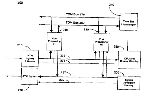
Figure 2 is a block diagram of an interworking device 200 consistent with this
invention. Device 200 includes six major components: (1) ATM Ingress and
Demultiplex
circuitry 210; (2) ATM Egress circuitry 220; (3) Voice-over-ATM (VoA)
processing modules
230; (4) TDM-based Time Slot Interchanger (TSI) 240; (5) CPU and control
circuitry 250;
and (6) Egress Contention Circuitry 255.
ATM Ingress and Demultiplex circuitry 210 receives ATM cells from ATM network
205, and sends each cell to the appropriate VoA processing module 230 via
busses 232 and
235. Each module 230 processes at least one type of VoA AAL. Interworking
occurs when a
VoA processing module 230 receives a specific VoA AAL. That module processes
the
information, places the resulting bytes into a TDM stream onto TDM bus 260
using the slots
reserved for that VoA module, and sends those bytes to TSI 240. TSI 240 then
places these
bytes onto TDM bus 270 in slots reserved for a different VoA processing module
230.
Module 230 takes the byte stream from bus 270, formats the bytes into a cell
with a different
VoA AAL, and sends the newly-created cell via busses 237 and 239 to ATM Egress
circuitry
220 for transmission out of device 200 to ATM network 205.
ATM Ingress and Demultiplex circuitry 210 may also modify the ATM cell header
(via VPI/VCI translation) or otherwise indicate to the receiving VoA module
230 the ATM
virtual channel to which the cell that the VoA module is processing belongs.
Circuitry 210
can also provide cell buffering, although buffering cells at this point in the
architecture can
produce "head-of line" blocking and thus may not be appropriate.
4
CA 02247588 1998-12-15
Figure 3 is an overall diagram of ATM Ingress and Demultiplex circuitry 210.
The
key design parameters for circuitry 210 are the number of VoA modules 230
possible in
device 200 and the total number of ATM VCs that device 200 receives. Ingress
and
Demultiplex circuitry 210 receives ATM data on line 310, a Start of Cell (SOC)
clock on line
320, and a 19.44 MHZ Receive Clock (RxClk) on line 325.
Circuitry 210 translates the network VPI/VCI numbers into a "triplet" of
identifiers:
VoA module number, VC number for that module, and an identification of the
type of data.
The data type indicates whether the data is voice, OAM, or signaling.
Preferably, if each
module can handle M virtual connections for voice, where M depends on the
module number,
the VC numbers range from 0 to M-1.
Figure 3 shows a possible implementation of circuitry 210. As shown, circuitry
210
includes a header extraction circuit 330 that finds the header of each packet
and examines the
VPI/VCI bits. Figure 3 shows header extraction circuit 330 as a shift register
with
components 331, 332, 333, 334, and 335. The SOC signal causes the latch 340 to
store the
VPI/VCI bits.
Control circuit 350 uses tables in SRAM 360 that relate the VPI/VCI bits for
the
different formats to corresponding VoA modules. Control circuit 350 helps load
SRAM 360
from an external processor (not shown) via,uP interface 380, latch 382, Write
Address line
384, and Write Data 386. The output of SRAM 360 is the VoA Module Selection
information sent via interface 370 to line 375. The received packets and SOC
pass from
header extraction circuit 330 onto lines 232 and 235, respectively.
Figure 4 is a block diagram show one possible implementation of VoA processing
module 230 consistent with this invention. Modules 230 preferably process the
following
VoA AALs: (1) the custom 48 DSO format shown in Fig. 1; (2) AAL-5 single call
per
CA 02247588 1998-12-15
channel; and (3) AAL-1 (simplified) single call per channel. As systems needs
change, so too
will the number and types of VoA modules.
In the ATM-to-TDM direction, each module 230: (1) receives ATM cells on busses
232, 235, and 375 from the ATM Ingress and Demultiplex circuitry and performs
any
necessary buffering for rate adaption; (2) performs appropriate AAL processing
on the cell
contents to extract the voice or n x 64 kbps transport bytes; (3) performs any
necessary cell
delay variation (CDV) dejittering; and (4) inserts transported bytes into
appropriate slots onto
the bus onto bus 260 for TSI 240.
Preferably, a FIFO and ATM interface 410 performs the interfacing and cell
buffer
functions. Cell buffering may be necessary if the VoA AAL processing cannot
process at the
full ATM line rate. Buffering also allows multiple, slower VoA processing
modules to be
used. Because the modules operate in parallel, however, they provide a higher
overall
throughput and allow a high degree of scalability.
ATM/AAL to TDM processing module 420 performs the appropriate AAL processing
on cell contents and CDV dejittering. The processing includes unpacking the
cells and
changing the order of the information in accordance with the corresponding
format. Each
module extracts the appropriate DSO bytes, or voice channels, according to its
associated
AAL. Processing and dejittering can occur in different orders depending on the
AAL being
processed. For example, a single call per channel would likely be dejittered
on the byte
stream after processing rather than on the ATM cell stream. In that situation,
CDV will be
typically much less than the cell fill delay, and cell-based dejittering would
be too crude and
would add unnecessarily long delays. For a low delay multiplex format,
however, dejittering
could occur before processing to reduce implementation complexity.
6
CA 02247588 1998-12-15
Interface circuitry 430 contains timing to ensure that the bytes were placed
onto bus
260 during the proper times. Such circuitry is well known.
In the TDM-to-ATM direction, VoA processing module 230: (1) extracts
appropriate
bytes from TDM bus 270; (2) assembles ATM cells in accordance with the AAL it
is
implementing; and (3) sends out ATM cells to the egress circuitry in
accordance with
received contention resolution information. The speed of TDM bus 270 must be
high enough
to serve all the VoA modules.
To reduce the need for expensive high speed circuitry and buffering on the TDM
interface, TDM slots can be assigned to VoA modules 230 nonconsecutively, such
as by
interleaving the slots among VoA modules 230 so that none has to process at
the peak TDM
bus rate. The design of a TDM interface circuit 440 is conventional, however,
just needing to
ensure that all bytes in the appropriate time slot of bus 270 are properly
received.
A TDM-to-AAL/ATM circuit 450 assembles the ATM cells appropriately according
to the corresponding AAL protocols. The design of this circuit is not
important to this
invention other than to ensure that it operates fast enough to keep up with
the byte stream.
An ATM interface circuit 460 in VoA processing module 230 can have many
different
designs. For example, it may either be completely distributed in VoA modules
230, have
minimal circuitry because the contention functions are completely centralized
in Egress
contention circuitry 255, or be partially distributed. The final design is not
critical to this
invention.
Figure 5 shows another implementation of VoA processing module 230. For
simplification, FIFO and ATM interface 410 and ATM interface circuit 460 are
shown as
FIFOs 510 and 520, respectively, and interface circuitry 430 and TDM interface
circuit 440
are shown as a single TDM interface circuit 530. ATM/AAL to TDM processing
module 420
7
CA 02247588 1998-12-15
and TDM-to-AAL/ATM circuit 540 are combined in an AAL1 SAR chip WAC-021 540
from Integrated Technologies, Inc. SRAM 550 provides temporary storage and
buffering for
chip 540.
Preferably, VoA processing module 230 handles the AAL1 formats of voice. This
block diagram could also represent an AALS VoA processing module simply by
replacing
chip 520 with any one of the AALS SAR chip available from, for example, NEC
Corporation,
Integrated Device Technology Inc., Connectware, and Toshiba Corp..
Figure 6 shows how circuitry from another manufacturer, Maker Communications,
can also function as VoA module 230. Along with FIFO 610 and TDM interface
circuitry
620, which is similar to corresponding circuitry shown in Figure 5, elements
630 and 640,
known as modules. MXT3010 and MXT3020, can handle AALO, AAL1, AALS, and
proprietary voice formats, although not necessarily all at once.
TSI circuit 240 can be a conventional component used in most DSO (voice and
64kbps) switching systems, PBXs, Central Office Switches, etc. Key criteria
for circuit 240
are the speeds of busses 260 and 270 and switching capacity. An appropriate
contention
resolution algorithm is needed, however, to avoid excessive CDV. TSI circuit
240 uses 8-bit
transmit and receive data buses plus control signals. Other TDM busses, such
as MVIP or
SCSA, could also be used .
CPU and control circuitry 250 is responsible for the following functions: (1)
general
I/O device initialization and configuration; (2) setting connection tables in
TSI circuit 240;
(3) setting up the ATM demultiplex tables and VPI/VCI translation tables in
ATM Ingress
and Demultiplex circuitry 210; (4) configuring VoA processing modules 230; and
(S)
configuring ATM egress contention resolution circuitry. In addition, control
circuitry 250
may be responsible for timing recovery and distribution.
8
CA 02247588 1998-12-15
Figure 7 shows a block diagram of Egress Contention Circuitry 255. Circuitry
255
arbitrates the access of VoA modules 230 to Egress Circuitry 220 and ATM 205.
Circuitry
255 receives the ATM bus clock and a TDM frame pulse clock and controls read
signals for
the various modules 230. One means of arbitration uses round-robin polling,
which works
well because the sum of the bandwidths at the output of VoA modules 230 is
less than or
equal to the bandwidth of the egress ATM bus 225 .
The main sizing for device 200 depends on the bandwidth of ATM busses 232,
235.
TDM busses 260, 270 should have at least the same capacity to avoid
underutilizing the ATM
link connected to device 200. Assuming that ATM link was an STS-3c ATM link at
155.52
Mbps, it can accommodate 2119 DSOs with a minimum overhead custom AAL,
assuming no
compression. Accordingly, TDM busses 260, 270 should support approximately
2000 DSOs
(e.g., 8 bits at 16.4 MHZ). Because signaling overhead and queuing effects
prevent the ATM
link from being fully used, the bandwidth of the TDM busses can be close to
the maximum.
ATM busses 232, 235, 237, 239 are preferably a standard UTOPIA parallel busses
used to connect ATM and AAL integrated circuits. Those busses are 8-bit
receive and
transmit buses that are clocked at a minimum of 19.44 MHZ (for STS-3c).
For egress contention with an STS-3c signal carrying ATM, slightly more than
44
cells can be transported every 125,u5, the byte time for a DSO signal.
Dividing internal ATM
UTOPIA bus 237, 239 into 44 slots, which is 99.6% efficient of STS-3c ATM
bandwidth,
allows use of a slightly lower byte clock of 18.66 MHZ synchronized to 125,u5.
In addition to this clock, Egress contention circuitry 255 generates a 125,uS
frame
clock and a SOC clock every 2.84,uS. All these clocks are synchronous so, for
example, a
frame always starts on a cell boundary. These 44 ATM egress time slots are
assigned to VoA
9
CA 02247588 1998-12-15
modules 230 based on their bandwidth needs. VoA modules 230 are responsible
for
scheduling egress on the slots that they have been assigned.
As is apparent from this description device 200 is extremely flexible and
scalable.
For example, one possible configuration for device 200 in Figure 1 is as
follows: (1) one VoA
module 230 handling the proprietary (ATM DS-48) format in Fig. 1, with a
capacity for 20
ATM VC and corresponding to 960 DSO; (2) one VoA module 230 handling
simplified AAL-
1 single channel adaptation (47 byte fill) with a capacity for 470 ATM VCs
(470 DSOs); and
(3) two VoA modules 230 handling AAL-S 40 byte fill single channel adaptation,
each
module with a capacity of 240 ATM VCs (240 DSOs). The VoA module 230 handling
the
proprietary (ATM DS-48) format requires one egress slot per ATM VC. The VoA
module
230 handling simplified AAL-1 single channel adaptation requires one egress
slot per 47
VCs. The two VoA modules 230 handling AAL-5 40 byte fill single channel
adaptation
requires one egress slot per 40 VCs. This configuration uses 42 of the 44
available egress
slots.
Other embodiments consistent with this invention will be apparent to those
skilled in
the art from consideration of the specification and practice of the invention.
The specification
and examples should therefore be considered as exemplary. The true scope and
spirit of the
invention are determined by the following claims.