Note: Descriptions are shown in the official language in which they were submitted.
CA 02248042 2001-04-11
1
OPTICAL DIFFRACTION GRATING
The present invention relates to an optical device suitable for use, for
example, as
a wavelength multiplexer/demultiplexer in an optical telecommunications
system.
BACKGROUND TO THE INVENTION
Bulk optic diffraction gratings are well known, and it has previously been
proposed
to use such gratings as passive multiplexers/demultiplexers in optical
networks employing
wavelength division multiplexing (WDM). The use of bulk-optic components tends
however to result in high packaging and maintenance costs. Accordingly, while
the use
of such components might be feasible if wavelength multiplexing/demultiplexing
was to be
confined to a few core switches, bulk optic components are not suitable for
more
widespread use in a network. Current interest in WDM centres on its use in
local access
networks in combination with optical time division multiplexing (OTDM) for
longer links in
the network. There remains a need therefore for a grating which is
sufficiently robust and
inexpensive to be used in local access loops throughout a network, and
possibly to be
present in each subscriber terminal.
The paper by Poguntke and Soole, "Design of A Multistripe Array Grating
Integrated Cavity (MAGIC) Laser", Journal of Light Wave Technology, Vol. 11
No. 12
December 1993, discloses a grating formed in an InP-based planarwaveguide
structure.
The grating is defined using photolithography and dry etched using, for
example,
chemically assisted ion-beam etching, to form a stepped wall extending
perpendicularly
through the planar waveguide. The grating is then metallised in order to
improve its
reflectivity. This structure, however, offers only limited angular dispersion,
and so is not
able to accommodate many wavelength channels without becoming unacceptably
large.
SUMMARY OF THE INVENTION
According to the present invention, there is provided an optical device which
includes:
a) an optical diffraction grating,
b) an optical input channel aligned to direct optical radiation onto the
waveguide for diffraction, and
c) one or more optical output channels the or each of which is aligned to
acquire optical radiation diffracted by the diffraction grating;
wherein:
i) said device comprises a waveguiding layer located between and in contact
with a first confining layer and a second confining layer,
CA 02248042 2001-04-11
2
ii) the grating is located in the central layer, and
iii) the grating takes the form of a planar array of scattering centres said
array
having 1 - 10 rows of scattering centres.
In preferred embodiments of the invention, the array has 1, 2 or 3 rows of
scattering centres. A single row of scattering centres may advantageously be
employed.
Each scattering centre preferably takes the form of a hole in the central
layer. Each hole
preferably contains a material responsive to an electric field, e.g. a liquid
crystal. Each
hole also preferably extends through the first covering layer, through the
central layer and
into the second covering layer, each hole containing filler material having a
refractive index
which is different from the refractive index of the rest of the central layer.
The central layer
is preferably formed of IIIN semiconductor and each hole contains a different
III/V
semiconductor. The first confining layer and the second confining layer are
preferably
formed of InP, the central layer is formed of InGaAsP and each hole contains
either InP
or GaInAs.
The input channel referred to above preferably includes a waveguide formed in
the
central layer and the or each output channel typically includes a waveguide
formed in the
central layer.
Preferred embodiments of the invention also include two or three rows of
scattering
centres and the spacing between the rows is such that, at a predetermined
wavelength of
operation, the grazingly emergent beam scattered from one row interferes
constructively
with the grazingly emergent beam scattered from the or each other row.
The term photonic crystalline material as used in the description of
embodiments
following denotes a material manufactured with a periodic variation in
refractive index,
having a periodicity of the order of magnitude of an optical wavelength. As
further
discussed below, such material is sometimes referred to as "photonic band gap
material".
The described embodiments use photonic crystalline material to provide a
grating
suitable for integration with other optical components and exhibiting high
dispersion and
efficiency. Photonic crystals are a class of material manufactured with a
periodic dielectric
structure. The behaviour of photons within such a structure is found to be
analogous to
that of electrons within a semiconductor. In particular it is found that there
are photonic
band gaps (PBGs) analogous to electronic band gaps in semiconductor crystals.
Photons
having wavelengths within the band gap range are forbidden to propagate. Most
work on
photonic crystals has focused on producing these photonic band gaps. However,
a novel
analysis by the present inventor has shown that photonic crystals exhibit
another property
CA 02248042 2001-04-11
3
which can be exploited to provide a highly efficient grating. It is found that
if the pitch of
the photonic crystal is selected so that the first order diffracted beam is
grazingly emergent
from the crystal, then the diffracted angle varies sharply with wavelength,
while the
diffracted beam has a relatively high output intensity, potentially equal to
20% or more of
the input optical intensity.
Preferably the region of photonic crystalline material is generally planar.
The
photonic crystalline material may comprise a generally regular array of
scattering centres
formed in a dielectric material, in which case preferably the array is a
minimal array no
more than 10 rows deep and preferably only 1, 2 or 3 rows deep. The scattering
centres
may comprise holes formed in a dielectric substrate.
While work on photonic band gap materials has previously aimed at producing
extensive 3-dimensional arrays, the present inventor has found that an
effective diffraction
grating can be formed from an array which is only a few rows deep and which
may
comprise just a single row. Where 2 or more rows are present, then preferably
the
spacing between the rows is such that, at a predetermined wavelength of
operation, the
grazingly emergent beam scattered from one row interferes constructively with
the
grazingly emergent beam scattered from the or each other row.
When the separation between rows is chosen so that in a preferred scattering
direction there is constructive interference, then the grating functions as a
highly efficient
fixed frequency filter and as such is particular valuable for use in WDM
systems.
Preferably the means for coupling light to and from the photonic crystalline
material
include waveguides formed on a common substrate with the photonic crystalline
material.
The waveguides may comprise planar structures, and may be arranged to confine
light in
the direction normal to the planar surface. It is particularly preferred that
the waveguide
should be a ridge waveguide arranged also to confine the beam in the plane
parallel to the
planar surface. The grating may be arranged to operate transmissively, with
the
waveguide for the input beam on one side of the photonic crystalline material,
and the
waveguide for the output beam on the other side of the photonic crystalline
material.
Alternatively, the grating may be arranged to function reflectively, in which
case the
means for coupling the input beams and the means for coupling the grazingly
emergent
output beam are located on the same side of the photonic crystalline material.
Preferably the dielectric material is a III-V material, and more preferably is
indium
phosphide.
CA 02248042 2001-04-11
4
The photonic crystal may comprise a regular array formed from two dielectric
materials of differing refractive indices. This structure may be formed as an
array of holes
in a first dielectric material with the holes filled with a second dielectric
material.
Alternatively, where the substrate includes, e.g., a quaternary waveguide
layer, then the
holes may be filled with the same material used to form the basis of the
substrate. An
alternative structure may comprise pillars of a first dielectric material
extending into air or
into a second dielectric material. One of the dielectric materials making up
the photonic
crystal may have a refractive index which is variable in response to an
applied control
signal. This may be an electro-optic material responsive to an applied
electrical field, or
a non-linear optical material responsive to an applied optical control signal.
The use of a material with a variable refractive index in the photonic crystal
enables
the grating to function as a tunable filter.
The diffraction grating described herein is not limited to use in
configurations in
which it is the grazingly emergent beam which is output. It may also be used,
for example,
in configurations in which the reflected beam is output, or in which a beam
diffracted at a
relatively larger angle is output.
The present invention also encompasses wavelength multiplexers and
demultiplexers including a grating in accordance with the preceding aspects of
the
invention.
DESCRIPTION OF THE DRAWINGS
Devices and methods of manufacture embodying the present invention will now be
described in further detail, by way of example only, with reference to the
accompanying
drawings in which:
Figures 1 a and 1 b are a plan and sectional side view respectively of a
grating
embodying the present invention;
Figure 2 is a diagram showing schematically the photonic crystal of the
grating of
Figure 1;
Figure 3 shows plots of reflection and transmission coefficients as a function
of
frequency for the photonic crystal of Figure 2;
Figures 4a and 4b are schematics of alternative photonic crystal
microstructures;
Figure 5 is a cross-sectional view showing the structure of the planar
substrate of
the grating of Figure 1;
CA 02248042 2001-04-11
Figure 6 is a schematic of a second alternative photonic crystal;
Figures 7a and 7b are sectional and plan views of a third alternative
photonic crystal;
Figures 8a and 8b are plots of reflection and transmission coefficients of
5 further examples of gratings embodying the present invention;
Figures 9a and 9b are plan and sectional views of a WDM demultiplexer;
Figure 10 is a plan view of an alternative embodiment of a WDM
multiplexer;
Figure 11 is a plot showing the polarisation dependence of reflection
coefficients of a grating embodying the present invention; and
Figure 12 is a plot showing the ratio of the reflection coefficients of
different polarisation states in the example of Figure 1 1.
DESCRIPTION OF XAh~p~ FS
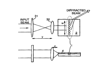
A grating comprises a region of photonic crystalline material 1 formed in a
mufti-layered planar substrate 2. An optical system comprising a first lens 31
with
a focal length of, e.g. 1 Ocm, and a second lens 32 with a focal length of,
e.g. 1 cm
collimates an input optical beam. The lenses 31,32 are separated by a distance
y
which is equal to the sum of the focal lengths. The lens 32 is spaced from a
facet
of the planar substrate 2 by a distance z of 1 cm in this example. The optical
system couples light into a waveguide layer 4 where it propagates to meet the
photonic crystal 1 with normal incidence. A grazingly emergent diffracted beam
is
transmitted through the photonic crystal 1 and propagated through the
waveguide
layer 4 and emerges from a side facet of the planar substrate. The emergent
beam
tends to diverge in the direction normal to the planar substrate. Optionally a
cylindrical fens may be used to collimate the emergent beam.
Figure 2 shows schematically the configuration of the photonic crystal 1.
fn this example, it comprises a linear array of holes formed in a substrate of
dielectric constant .13 with a pitch of 0.57um. As shown in the diagram, a
normally incident input beam with a wavelength of around 1550 nm is diffracted
by the photonic crystal to produce grazingly emergent transmitted and
reflected
beams. In addition, part of the beam passes straight through the photonic
crystal
without diffraction, and part is reflected. The width of the grating w is in
this
example 800 microns, the distance from the input fibre to the grating is 4mm
and
CA 02248042 2001-04-11
6
the distance from the grating to the output is 4mm. For ease of illustration,
only a
relatively few holes are shown in the Figure. In practice, as further
discussed
below, the array may comprise a row of 1000 or more holes.
Figure 3 shows the reflection and transmission coefficient for the
normally incident beam as a function of frequency normalised to 1.55um. Plot a
is
the transmission coefficient, b is the reflection coefficient and plots c and
d ara the
coefficients of the transmitted and reflected diffracted beams respectively.
The
onset of grazing emergence is seen in plots c and d at a normalised frequency
of
around 0.8 and is marked by the dashed line. As set out in the theoretical
analysis
below, it is found that the grazingly emergent beam at angles of a few
degrees,
say 3 to 5 degrees, has a practically useful level of optical power and
emerges at
an angle which varies rapidly with wavelength.
As an alternative to use with a normally incident beam, the grating may be
used with a beam incident at an angle of, e.g., 30 degrees. Plot 3b shows the
reflection coeffiecients in this case. In this case the grazingly
emergent output beam for a given wavelength will have different diffraction
angles
on either side of the normal to the plane of the photonic crystal.
The pitch and hole size of the array, and the angle of incidence, may be
varied according to the refractive index of the substrate material and the
desired
wavelength range in which the grating is to be used. Figures 8a and 8b are
graphs
showing the performance of gratings constructed with different pitches and
angles
of incidence. Figure 8a is for a grating with a pitch of 0.47 microns used at
normal incidence. Figure 8b relates to a grating with a pitch of 0.3i 3
microns
used with a beam incident at an angle of 30 degrees to the normal. The hole
radius
in each case is 0.17 microns in 8a and 0.1175 microns in 8b. In both cases,
the
dielectric constant of the substrate is 10.9, giving a refractive index of
3.3.
The holes need not have a circular cross section and may, for example,
have a cross section which is generally square.
In the present examples, the array of holes making up the photonic crystal
are produced by reactive ion-beam etching (RIE) in a planar InP substrate.
Figure 5
shows in detail the structure of the planar substrate.
The process of manufacture can be broken down into two stages: an
epitaxy or deposition stage, and a subsequent stage in which the
microstructure is
CA 02248042 2001-04-11
7
etched. In the first stage, a waveguiding layer is fabricated on InP
semiconductor
material by a series of epitaxial depositions using the Metal-Organic Vapour
Phase
Epitaxy (MOVPE) technique. This first stage includes the following steps:
1. A buffer layer of 1000nm thickness of InP is deposited;
2. A waveguiding layer 300nm thick of InGaAsP is deposited - the
composition of the InGaAsP is such that it has a bandgap wavelength of
approximately 1.3 microns;
3. A cladding Payer 300nm thick of InP is deposited.
All the deposited materials are nominally pure, i.e. undoped.
IO Subsequently, in the second stage, microstructures are etched into the
wafer. This is done using reactive ion etching. Direct write technology is
used to
create the mask directly on the sample. The second stage involves the
following
steps:
1. The sample is briefly cleaned in acid and then a 100nm thick layer of
silicon nitride Si3N4 is deposited.
2. A layer of photoresist which is known as "ebeam resist" and which is
sensitive to an electron beam is spun onto the sample to a thickness of
approximately 500nm. In this case, the resist used is that manufactured by
Nippon Zeon and known as ZEP520*
3. The resist is exposed in the desired microstructure pattern using electron
beam lithography.
4. The resist is then developed. This dissolves the exposed areas. The
unexposed ZEP520 remains and forms a mask which is used in the following
stages.
5. Reactive ion etching using CFQ etches into the silicon nitride layer. This
transfers the the mask pattern from the resist layer to the silicon nitride
layer.
6. The sample is cleaned in two stages. The unexposed resist is removed,
and then the polymer which results from the RIE process is removed.
7. The main RfE process is carried out. The patterned silicon nitride layer
acts as a mask. The etching mixture consists of methane/hydrogen/oxygen. This
mixture preferentially etches the InPIInGaAsP rnateria( over the silicon
nitride mask.
8. The polymer resulting from the RfE process of step 7 is removed.
* Trademark
CA 02248042 2001-04-11
8
9. The sample is thinned from approximately 0.5mm thickness to
approximately 150 microns thickness. This makes possible easier cleaving of
individual samples. The individual samples are nominally 1x1 mm2. The grating
microstructure bisects the samples parallel to the sides.
It will be understood that the above process is described by way of
example only, and that a variety of other processes may be used. For example,
methane/hydrogen RIE may also be used. The etching may be followed by
regrowth to fill the holes with a second dielectric material having a
different
refractive index to the substrate. Figure 6 is a schematic of a photonic
crystalline
region formed in this manner. In this example, the holes in the waveguide are
filled
with a III-V semiconductor material such as InF itself, or a ternary e.g.
GaInAs.
The material used to fill the holes may have a refractive index which is
variable in
response to an applied control signal. For example, it may comprise a liquid
crystal
material. The refractive index of the fill material then varies in response to
a
control voltage applied to a gate overlying the photonic crystal, allowing the
grating to be tuned to a desired wavelength. Alternatively, the fill material
may be,
e.g., a semiconductor chosen to have a strong optical non-linearity. In this
case
its refractive index is controlled in response to an applied optical control
signal.
Figures 7a and 7b show a further alternative structure for the photonic
crystal. In this example, the scattering centres are pillars 71 of the
substrate
structure, extending into air. This structure may be produced by an RlE
process as
described above for, the first example. The process is modified in that prior
to the
etching step, the silicon nitride photoresist is exposed everywhere except in
the
regions which are to form pillars. Then in the etching step, in the region 72
around
the pillars the substrate is removed down to a depth of e.g. 0.7 microns
leaving
the pillars free-standing in a narrow trough in the substrate. It should be
noted
that although in this example the pillars, and in previous examples the holes,
have
had a circular cross-section, this is not essential for the functioning of the
grating,
and that scattering centres having other less uniform shapes may be used. For
example the cross-section may be generally ellipsoid, and may vary in size at
different depths through the hole or pillar. This allows the use of etching
processes which may not produce perfectly regular shapes.
CA 02248042 2001-04-11
9
The present invention is by no means limited to the use of photonic
crystals in the form of one-dimensional arrays as in this first example.
Figure 4a
shows schematically an example using 2 rows of holes, with the separation
between the rows selected so that the path difference 8 is equal to an integer
number of wavelengths, giving constructive interference of the diffracted beam
for
the design wavelength. This constraint can be expressed algebraically as l =
b( 1-
sin(90-~)) where b is the separation between the rows and ~ is the diffraction
angle. It can been seen that the use of two more rows has the effect of adding
a
preferred direction to the diffraction. That is, while the simple 1-
dimensional array
either transmits or reflects the diffracted order, the modified 2-dimensional
structure reinforces either the reflected or the transmitted order, depending
on the
distance b. A structure formed in this way functions as a fixed wavelength
filter.
For the 1-dimensional structure there is also a constraint on the array
pitch, wavelength and diffracted angle of the form ~. = a cos ~. Where a 2
dimensional structure is used, so that the constraint of the first equation
above
also applies, then there is a solution only for a single wavelength. The 2-
dimensiona( structure can therefore be engineered to act as a fixed filter for
one
particular wavelength. The use of multiple rows of scattering centres is
particularly preferred when the scattering centres are relatively weak in
effect.
This is the case if, for example, the holes etched in the substrate are
relatively
shallow and stop short of the waveguide layer or if they are filled with a
second
dielectric material having a refractive index close to that of the substrate.
In this
case more than a minimal array of holes may be required to produce a
diffracted
beam of sufficient power, and the array may be, for example, 10 or 15 rows
deep.
Figure 4b shows an example of a lattice which is 6 rows deep. This 2-D
lattice has two main sets of parallel planes, one running vertically and the
other
running approximately horizontally. The lattice is designed to obtain non-zero
order
diffraction from one set of planes, and wroth order diffraction from the other
set.
The condition is applied that both sets of planes should give rise to
diffraction in
the same direction. Therefore to obtain zero order diffraction (specuiar
reflectionl,
the planes running approximately horizontally should be angled such that their
normal bisects the angle between the input beam and the output beam. The
spacing of these planes is not critical, but it can be advantageous to space
them
CA 02248042 2001-04-11
so that the microstructures along the planes have a separation sufficiently
small
that only zero order diffraction results. The planes running approximately
horizontally have in general a separation less than the separation of the
microstructures in the 1-D array considered originally. The following
condition
5 applies for first order diffraction:
sinA + sink = n~,/d
where n is the order, ~. is the wavelength, d is the separation of the planes
or
structures, and B and ~ are the angles of incidence of the incoming and
outgoing
beams. A structure which is formed in this way is not limited in operation to
a
10 single wavelength, but reinforces and diffracts different wavelengths
through
different angles. It is therefore suitable, for example, for use as a
wavelength
division mulitplexing (WDM) demuitipfexer.
For the purposes of illustration, the above discussion treats the photonic
crystal as comprising weak scattering centres, producing Bragg diffraction. In
reality, the scattering centres in general produce strong scattering. The
present
inventor has carried out a novel analysis of a one-dimensional array of strong
scattering centres, which is set out below.
The derivation of the dispersion equation for a planar photonic crystal will
first be described. Let k; and kd be the wavevectors for the incident and
diffracted waves and g a reciprocal lattice vector for the periodic variation
of the
refractive index which is the essential aspect of the grating. Because the
electromagnetic fields that constitute the incident and diffracted waves must
belong to the same irreducible representation of the group of translational
symmetry operations for the grating, then
kd.g=~k;+g~g (1)
where g is the unit vector along g ie parallel to the grating. Denoting by 6;
and 8d
the angles the incident and diffracted beams make with the normal to the
grating
and by k = ~ the magnitude of the wavevector of the light ( ~, is the
wavelength
of the fight in the medium either side of the grating ) the equation ~ 1 ) may
be
written ksinAd=ksin6;+2~ (21
a