Note: Descriptions are shown in the official language in which they were submitted.
CA 022480~9 1998-09-23
577-286
IMPROVED CHIP CARD CONNECTOR
FIELD OF THE TlWENTION:
The present invention relates generally to an electrical connector which supports an
integrated circuit (IC) card to a printed circuit board. More particularly, the present invention is
5 directed to a chip card connector which provides for the easy insertion and removal of the chip
card from the connector.
BACKGROU~D OF THE INVENTION:
The electronic industry has seen growth in the use of flat plastic cards incorporating
10 computer chips therein. These chip or IC cards are also commonly referred as to as "smart
cards". A smart card is a card incorporating at least one electronic component to which electrical
cormection must be made. These cards include contact pads so as to allow electrical connection
to the electronic component on the card. Smart cards are commonly used in various consumer
oriented apparatus and m~chinPs such as telephones, bank machines and the like.
One particular type of smart card commonly used in telephones, especially cellular
telephones, is a mini-card or a mini-SIM (subscriber identity module) card. These cards have a
particular industry-accepted standard for size, shape and location of the electronic components
and contact pads. These mini-SIM cards are typically installed in the app~dlus, such as the
20 cellular phone, by a trained installer.
CA 022480~9 1998-09-23
~ . .
In order to effect electrical connection between the mini-SIM card and a printed circuit
board within the cellular phone, an electrical connector is employed. These connectors also are
m~nnf~tured in an industry-accepted configuration so that the mini-SIM card may be
accornrnodated by the connector. However, for various purposes, such as for example, to change
5 the subscriber identity, it may be necessary to replace the mini-SIM card within the phone. Thus,
the electrical connector used to support the mini-SIM card in the phone must permit the easy
replacement of cards therein. The art has seen numerous electrical connectors specifically
designed for use in removably connecting various types of smart cards.
U.S. Patent No. 5,603,629 discloses a connector for a mini-SIM type smart card having a
base supporting a plurality of electrical contacts. The base is mounted to a printed circuit board
in the phone. A cover is pivotally attached to the base and includes a slot for retention of the
card therein. The cover may be pivotally closed onto the base to place the pads on the card in
electrical connection with the contacts held in the base. The cover is movable from an open
15 position pçnnitting insertion and removal of the card to a closed position establishing such
electrical connection.
U.S. Patent No. 4,820,186 provides another example of a smart card connector having a
cover which pivotally mounts to the base. The card may be inserted and removed from the cover
20 from an open position. The cover is pivotally rotated to a closed position establishing electrical
connection with the contacts in the base. The cover is spring loaded with respect to the base so
as to mechanically lock the cover to the base in the closed position.
CA 022480~9 1998-09-23
U.S. Patent No. 5,320,552 also describes a smart card connector having a cover for
accommodating the smart card and which is pivotally mounted to a base. In addition to the cover
being pivotally movable with respect to the base so as to move the smart card into connection
with the contacts in the base, the cover is also movable linearly movable over the smart card to
5 lock the cover to the base.
In each of the above-referenced patents, electrical connection is established between the
contact pads of the card held in the cover and the electrical contacts supported in the base, by
simple pivotal movement of the cover with respect to the base. Once the cover is pivoted down
10 onto the base, electrical connection is established. Locking of the cover to the base is done in a
separate sequential operation.
During in~t~ tion it is quite cornmon for the installer to select a particular IC card from
a plurality of cards which is being carried by the installer for in~t~ tion into a particular
15 connector. As a result of transporting, h~n(llin~ and in~t~lling such a card, there is a tendency for
the contact pads on these card to accnm~ te dust and debris. Such accumulation may adversely
effect the h~te.co~ ection between the contact pads on the card and the contacts in the connector.
Simple rotational movement of the card into engagement with contacts of the base does little to
assure clean connection therebetween. Furthermore, as the cover is locked to the base in a
20 separate operation, mechanical connection of the card to the connector is not always assured even
where electrical connection is established. Over time the chip card could dislodge from the
connector without prior warning.
CA 022480~9 1998-09-23
It is therefore desirable to provide an electrical connector for accommodating a smart card
which establishes electrical connection by wiping the contact locations of the card upon
connection of the card with the contacts in the base.
5 SUMl\~ARY OF THE INVENTION:
It is an object of the present invention to provide an electrical connector for insertably
connçcting a chip card.
It a further object of the present invention to provide an electrical connector which
10 supports an IC card for movement into connection with contacts supported by the connector.
It is still a further object of the present invention to provide an electrical connection for a
chip card which provides for wiping engagement between the contact locations on the chip card
and the contacts of the connector to assure proper electrical connection therebetween.
In the efficient ~tt~inment of these and other objects, the present invention provides an
electrical connector for connecting contact pads of a IC card to a printed circuit board. The
connector includes a connector housing having a base supportable on a printed circuit board and
a cover movably supported to the base. A plurality of elongate electrical contacts are supported
20 by the base. Each contact includes a spring element for deflectable electrical engagement with
the contact pads of the IC card and contact tails exte~ciing from the base for termination to the
printed circuit board. The IC card is insertably supported by the cover for movement therewith.
.. . . ...
CA 022480~9 1998-09-23
The cover is pivotally movable from an open position permitting insertion and removal of the
card from the cover to a closed position. In such closed position the contact pads of the IC card
are positioned adjacent but not in full electrical engagement with the spring elements. The cover
is then linearly movable from the closed position to a locked position, for locking of the cover to
5 the base and for moving the contact pads of the IC card over the spring elements and into wiping
electrical engagement therewith.
As more particularly described by way of a preferred embodiment herein, the connector
includes a card support means on the cover for supporting IC card therein. The card support
10 means includes a plurality of ret~ining members formed integrally with the cover. The card
support means and the cover define a slot for the insertion and the removal of the card therein.
BRIEF DESCRIPTION OF THE DRAWINGS:
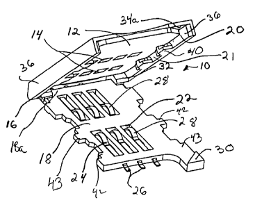
Figure 1 is a front perspective showing of the connector of the present invention
15 including a cover and a base with the cover shown in the open condition for insertion and
removal of a chip card.
Figures la and lb are top perspective and side elevational showings respe~;Lively ofthe
connector base of Figure 1.
Figure 2 is a top plan view of the connector of Figure 1.
CA 022480~9 1998-09-23
Figure 3 is a sectional showing of the connector of Figure 2 taken through the lines III-III
thereof.
Figure 4 is a front perspective view of the connector of Figure 1 shown with the cover in
S the closed position with respect to the base.
Figure S is a top plan view of the connector of Figure 4.
Figure 6 is a cross-sectional showing of the connector of Figure S taken through the lines
10 VI-VI thereo~
Figure 6a is an enlarged partial sectional view of the connector of Figure 6.
Figure 7 is a front perspective view of the connector of Figure 1 with the cover shown in
15 the locked position with respect to the base.
Figure 8 is a top plan view of the connector of Figure 7.
Figure 9 is a cross-sectional view of the connector of Figure 8 taken through the lines rx-
20 lX thereof.
Figure 9a is an enlarged partial sectional view of the connector of Figure 9.
CA 022480~9 1998-09-23
Figure 10 is a boKom perspective view of the cover of the connector of Figure 1.
Figure 1 1 is a vertical sectional showing of the cover of Figure 10.
Figure 12 is a boKom plan view of the cover of Figure 10.
DETAILED DESCRIPTION OF THE PREFERRED El\/IBODIlUENT:
As shown in Figures 1-3 the present invention provides an electrical connector 10 which
may be used to mechanically and electrically connect a chip card 12 to a printed circuit board
10 (not shown). The present invention has particular utility in mechanically and electrically
connecting chip cards of the type known as smart cards which provide an electronic component
on the card which is electrically accessible by electrically conductive contact pads 14 on one
surface of the chip card 12. The particular embodiment of the chip card shown herein is a mini-
SIM card and connector 10 may be particularly used in consumer accessible electronics, more
15 particularly cellular phones. It is desirable to insert and remove chip cards 12 from connector 10
for various purposes such as to change the subscriber's identity with regard to a particular
cellular phone. Accordingly, the connector of the present invention is designed to provide ease
of insertion and removal of the chip card 12-with respect to connector 10 and also to provide
reliable mechanical and electrical interconnection therewith.
Connector 10 of the present invention includes a two-part connector housing 16 including
a base 18 and a cover 20 mounted to base 18. Housing 16 may be formed of suitable insulative
.. . . .
CA 022480~9 1998-09-23
plastic. Base 18 is generally an elongate flat planar member having a plurality of apertures 22
therethrough. Base 18 ~U~JpOll~i a plurality of electrical contacts 24 within a~ s 22. Contacts
24 are formed of an electrically conductive material and are elongate members having oppositely
directed contact tails 26 extending from base 18 for solder connection to the printed circuit
board. Contacts 24 further include at the end opposite tails 26 spring contact elements 28
exten~ling above the plane of base 18. Spring contact elements 28 are design~d for resilient
electrical engagement with the contact pads 14 of chip card 12 as will be described in further
detail hereinbelow.
Base 18 includes a polarization tab 30 at one corner thereof for polarized accommodation
of chip card 12 preventing chip cards from being positioned in connector 10 in an incorrect
orientation. Base 18 further includes at one end 18a thereof a pair of transversely spaced
shoulders 32 which extend upwardly from base 18. Shoulders 32 provide for movable
accommodation of cover 20 on base 18 in a manner which will be described in further detail
hereinbelow. Base 18 also includes a pair of spaced apart laterally projecting ears 43 along each
longitudinal side thereof. Ears 43 define spaces 50 therebetween.
Cover 20 is generally an elongate member having a planar cover wall 34 and a pair of
parallel side walls 36 depending from cover wall 34. Cover 20 is of size and shape so as to
accornmodate chip card 12 along an undersurface 34a of cover wall 34. Cover 20 further
includes a downwardly directed central foot portion 38 at one end 20a which provides a
mechanical stop and a seat for an end 12a of chip card 12 as it is inserted into cover 20. The side
CA 022480~9 1998-09-23
walls 36 of cover 20 each include a pair of longitudinally spaced inwardly directed ledges 40
which are spaced a distance from the undersurface 34a of cover wall 34. The sp~cing between
ledges 40 and undersurface 34a is slightly larger than the thickness of chip card 12 so as to form
slot 21 for accommodating chip card 12 therein.
s
With additional reference to Figures 10, 11 and 12, undersurface 34a of cover 20 also
includes a downwardly directed central protrusion 42. Protrusion 42 extends in a direction
towards ledges 40 so as to decrease the effective width of slot 21 defined therebetween, so as to
provide frictional retainrnent of the chip card 12 when it is inserted therein. Such frictional
10 retaining ofthe chip card 12 helps positionally stabilize the chip card as the cover 20 is closed
onto base 18 as will be described in further detail hereinbelow.
Cover 20 further includes adjacent end 20a a pair of inwardly directed pivot pins 44
which are d~si~ne~l for accommodation within channels 46 of shoulders 32 of base 18. As more
15 particularly show in Figures la and lb, the charmels 46 include a pair of spaced-apart pin
receiving recesses 46a and 46b. These recesses permit the accommodation of cover 20 on base
18 at two longit~.1in~lly spaced locations.
Having generally described the connector 10 of the present invention, its operation may
20 now be described with respect to the figures. As shown particularly in Figures 1 and 2, cover 20
is shown in the open position with respect to base 18. In this position, the pivot pins 44 of cover
20 (Figs. 10 and 12) are positioned within rear recess 46a of channels 46 (Fig. lb). The cover 20
CA 022480~9 1998-09-23
is pivoted to a position with respect to base 18 approximately shown in Figures 1 and 3. In this
position, the chip card may be inserted into the slot 21 defined between the undersurface 34a of
cover wall 34 and the protruding ledges 40 from sidewalls 36. The chip card 12 is inserted until
the end 12a of the chip card abuts against depending foot portion 38 as shown in Figures 2 and 3.
The cover 20 is then pivoted down towards base 18 about pivot pins 44 so that the ledges 40
reside in respective spaces 50 between ears 43 of base 18.
The cover is now in closed position as shown in Figures 4-6a. Upon the pivotal closure
of cover 20 with respect to base 18, the end 12a of chip card 12 may ride along the inwardly
tapered upper surface 32a of shoulder 32 in a ramplike fashion. This will cause some slight
forward movement of chip card 12 within the slot 21 of cover 20 until it is located at a position
shown in Figures 6 and 6a with the end 12a of chip card 12 spaced a distance d, from the
depending foot portion 38. As shown in Figure 6, in the closed position, the contact pads 14 are
positioned adjacent to but not in full electrical engagement with the spring contact elements 28 of
contacts 24.
The chip card 12 is held in frictional engagement within cover 20 moving only under the
ramped urging of tapered upper surface 32a-of shoulder 32 by the frictional engagement of the
chip card 12 with protrusion 40 exten~ing from the undersurface 34a of top wall 34. Such
frictional engagement is sufficient to prevent unwanted movement of the chip card 12 within the
slot 21 of cover 20 yet permit the chip card to be ramped forward upon pivotally closing cover
20.
... . .
CA 022480~9 1998-09-23
After the cover 20 achieves the closed position shown in Figures 4-6, the cover may be
locked to the base to mechanically secure the cover to the base and further to move the contact
pads 28 in a wiping action over the spring contact elements 14 and into electrical engagement
therewith.
Referring now to Figures 7-9a, the locked position of cover 20 with respect to base 18 is
shown. In this position, the cover 20 is moved linearly with respect to base 18 in the direction of
arrow A so that the pivot pins 44 move out of rear recess 46a and into front recess 46b (Figure
lb). A light snap engagement is m~int~ined between pivot pins 44 and recesses 46a and 46b.
This snap engagement may be overcome by manual force. Such longitudinal movement causes
re-engagement of depending foot portion 38 with the end 12a of card 12 so as to urge or carry the
card forward a distance d2 in the direction of arrow A and to place the contact pads 14 into
wiping electrical engagement with the spring contact elements 28 of contacts 24. Such wiping
movement provides sufficient frictional engagement, due to the spring bias of the spring contact
elements 28, to remove any dust or debris which may exist at the interface of spring contact
elements 28 and contact pads 14. In addition to placing contact pads 14 into electrical
engagement with spring contact elements 20, such fol ~d movement in a direction of arrow A
serves to mechanically lock the cover to base 18. Downwardly directed ledges 40 are configured
to frictionally accommodate ears 43 of base 18 upon such linear movement of cover 20 so as to
latch with the ears 43 to thereby mechanically secure the cover 20 to the base 18 preventing the
cover from being pivotally opened in the locked position. Such locking of cover 20 to base 18
CA 022480~9 1998-09-23
assures the maintenance of electrical engagement between contact pads 14 and spring contact
elements 28 as well as positionally retains chip card 12 within connector 10.
As mentioned above and as shown in Figures 6 and 9, full electrical engagement between
pad 14 of chip card 12 and spring contact elements 28 of contacts 24 is not established until
cover 20 is locked to base 18. However, owing to tolerances in the m~nllf~ctl-re of chip cards 12
and connectors 10, slight intermittent non-electrical engagement of pads 14 to spring contact
elements 28 may be achieved in the closed but unlocked position (Figure 6). It is, however, only
upon locking of cover 20 to base 18 (Figure 9) that positive electrical engagement is achieved.
In order to remove chip card 12 from connector 10 for repair or replacement, the cover 20
is moved linearly rearward in a direction opposite arrow A (Fig. 9). The pivot pins 44 move out
of forward recess 46b and into rear recess 46a. Once cover 20 is moved to this position, the
ledges 40 of cover 20 clear the ears 43 of base 18. This allows the cover to be pivoted upwards
to a position shown in Figures 1, 2 and 3. In this position, the installer may m~ml~lly grasp the
opposite edge 12b of card 12, access being provided by an undercut 52 in the leading edge of
cover 20. The installer may then repair or replace chip card 12 and reconnect the chip card in
connector 10.
'0 The present invention provides superior electrical connection between the contact pads 14
of chip card 12 and the spring contact elements 28 of contacts 24 in base 18 by providing for
wiping engagement therebetween. Such wiping engagement is provided by moving the chip card
12
. CA 022480~9 1998-09-23
with the cover 20 in a linear direction from a closed but unlocked position to a locked position.
Furthermore, assurance is provided that the chip card is properly secured within the connector as
unless locking engagement is provided between the cover and the base, the contact pads of the
chip card will not be in full operating electrical engagement with the contacts 24 of the base.
Such positioning may not provide proper electrical functioning of the device. It is only upon
locking of the cover to the base that the pads of chip card will be in full electrical engagement of
the contacts of the connector.
While the particular embodiment of the present invention has been shown and described,
it will be obvious to those skilled in the art that changes and modifications may be made without
departing from the teachings of the invention. The matter set forth in the foregoing description
and accolnp~lying drawings is offered by way of illustration only and not as a limitation. The
actual scope of the invention is intended to be defined in the following claims when viewed in
their proper perspective based on the prior art.