Note: Descriptions are shown in the official language in which they were submitted.
CA 0224831S 1998-09-04
PCT/EP 97/01096
CSELT Centro Studi e Laboratori
Telecomunicazioni S.p.A.
Torino, Italy
PROBE FOR FAULT ACTUATION DEVICES
The invention described herein relates in general to the so-called fault actuation or
insertion techniques used to test the operation of electronic equipment, and concerns a
S probe for fault actuation devices, arranged to force a test point of an electronic equipment
under test to a given signal level, the probe comprising: a transistor having a control
electrode and two circuit terminals, which circuit terminals are connected respectively to
said test point and to said given signal level, and control means acting on the control
electrode of the transistor to selectively switch the transistor between a cut-off condition
and a conducting condition~
A probe with some similarity to the above probe is known from E~-A~ 261 367. Theprobe is a mechanical probe which is brought in electrical contact with a test point of an
electronic component and an alternating sguare wave test signal is applied to the test
point through a transistor and extracted through a circuit connected to the probe. The
transistor which is a field effect transistor applies to the test point the mentioned variable
signal, so as to simulate regular operation conditions of the component. Parasitic
c~p~cit~nces within the transistor are likely to introduce some distorsion into the a~mplified
square-wave voltage.
In electronic equipment and systems (especially if very complex: by way of non
limiting example, reference can be made to switching exchanges of telecommunications
networks), the need often arises to check the behaviour of the equipment and of the
system in the presence of particular fault conditions This check can be carried out not
AMEN~E~ S~EET
CA 0224831~ 1998-09-04
2 ' J ,~
- only in the testing phase, but it may be a part of the fault diagnosis and/or identification
or of automatic reconfiguration functions which often are provided for in such equipment
and systems to ensure that the equipment can still operate (at least in part) even i~ the
presence of faults.
In digital equipment, the types of fault to be actuated or inserted (hereafterthe terms
"actuation" and "insertion" shall be used as synonyms) at the hardware level generally
entail forcing certain points of the equipment to a pre-set signal level, corresponding for
example to a logic "O" or to a logic "1". A solution conventionally adopted in the art has
thus been to establish, in correspondence with the point to be forced to the pre-set signal
level, an electrical connection (usually by means of a jumper) towards the ground level
or a given power supply level (+Vx or -Vcc).
This solution is not particulariy easy to be put in practice, also in view of its
intrinsically "fixed" nature: once the jumper has been applied, the point involved is
constantly maintained at the signal level to which the jumper is connected. Hence, it is
not possible quickly to monitor the reaction of the equipment at the moment the fault is
inserted and/or, which can be of no less interest, at the moment the fault is eliminated.
To overcome these drawbacks, a solution has been proposed, at least at the
experimental level, which entails connecting electrical conductors, coming out of the
equipment under test, to the fault insertion points. Such conductors lead to a set of
electromechanical switches (such as, typically, relays) which allow the requiredconnections to the reference voltages to be established.
This solution cannot be considered fully satisfactory, for several reasons.
First, it is intrinsically cumbersome. Additionally, the conductors connected to the
fault insertion points always disturb the equipment being tested. Thus, the fault conditions
simulated for the test do not exactly correspond, from the electrical point of view, to the
fault conditions likely to occur in the equipment (this is particularly true when current
absorption at the fault point is also to be measured). Further, the conductors disturb the
operation of the equipment even under regular service conditions, i.e. when there is no
fault actuation.
Thus, there is a need to provide a solution capable of overcoming the probtems set
out above and in particular a solution which:
- makes reproducing fault conditions very flexible, in order to allow a substantially
instantaneous switching from the normal operating condition to the simulated fault
condition of the equipment under test;
AMEND~D ~ EET
CA 0224831~ 1998-09-04
- does not disturb the operation of the equipment both when a fault is being simulated
and under normal operating conditions of equipment, with no faults applied,
- is intrinsically not cumbersome, in order to allow simuitaneous or neariy simuitaneous
fault insertion into a number of points of an equipment under test, for instance points
sbelonging to a board inserted in a cabinet, according to a typical constructiveembodiment of complex electronic equipment, and
- allows automating testing operations.
Additionally, it should also be noted that the devices required, at least as concerns
the components (probes) directly used for connection to the equipment under test, should
10have.a negligible cost: thus they can be left in place once the test has been completed,
that is, they can be single-use products.
According to the present invention, this goal is reached thanks to a device as stated
in the above preamble, which device is characterized in that in its conducting condition,
the transistor in use, is driven into saturation condition, causing, said test point to be
15forced to said given signal level, and a capacitor is directly connected between the control
electrode and the circuit terminal of the transistor opposite to that point, which capacitor
has a substantially higher capacitance value than the value of the parasitic capacitance
existing between control terminal and the circuit terminal of the transistor coupled to the
test point.
20From DE-B-23 63 360, it is known per se that, in this case in an amplifier, a series
connection of a capacitor and a resistor is coupled between the base and the emitter of
the amplifier transistor. The resistor is a part of a voltage divider. The transistor used as
an amplifier operates in a linear zone of its characteristics in order to provide an output
signal proportional to the input signal. The known circuit arrangement, thus, does not give
25any hint to the person in the art to arrange the probe for fault actuation in the manner
proposed by the invention.
Within the concept of the invention, the construction details may be changed widely
with respect to what will be termed transistor, working as an electronic switch. The
"transistor" may be any electronic component with equivalent operating characteristics
30The term "transistor" thus is to be taken to include such equivalent electronic de\~ices as
well; this also holds true for the terms ~collector", ~emitter~ and ~base", identifying the
terminals of a bipolar transistor.
The invention shall now be described, purely by way of non-limiting example, with
reference to the enclosed drawings, wherein:
ND~3~
CA 0224831S 1998-09-04
3a
- Figure 1 depicts, as a general block diagram, the typical configuration of a fault
actuation device, in conjunction with an equipment tested by using such a system,
- Figures 2 through 5 show circuit'diagrams of four different embodiments of a probe
for fault actuation devices according to the invention, and
s - Figure 6 represents an example of practical construction of a probe according to the
invention.
In Figure 1, A denotes the whole of an electronic equipment to be tested according
to typical fault insertion procedures. By way of non-limiting example, equipment A could
be a digital switching exchange of a telecommunications system or a part of thatexchange (for irlstance the set of circuits located on a board C). In the same Figure,
references Pl, P2 indicate, by way of example, two points of board C where a fault is to
be inserted. Of course any number of points throughout the equipment can be involved,
depending on the application requirements. As it has already been stated, inserting a fault
entails, in practice, forcing the point involved (hereafter generally indicated as Pi) to a pre-
set signal level, for instance O V (ground voltage) or +~ V (i.e. a +Vx power supply
voltage). The signal levels indicated usually correspond, in a digital equipment, to logic
levels "O" and "1".
Equipment A is usually associated with a system A1 (forming an integral part of the
equipment) for identifying/diagnosing faults and/or for reconfiguring equipment A to make
it resistant to the onset of particular faults. The features of such a system are known in
themselves to those skilled in the art, and they do not require to be illustrated specifically
herein, since they are not of interest for the understanding of the invention.
As previously indicated, the invention specifically faces the problem of inserting a
fault into a specific point Pi, regardless of the reaction induced by the fault insertion into
~5 equipment A and of the monitoring of that reaction.
CA 0224831~ 1998-09-04
WO 97/33180 4 PCT/EP97/01096
Fault insertion into point Pi is accomplished by a device 1 comprising one or more
probas 10 (possibly of the single-use type) which form the specific subject matter of the
present invention. In practice, device 1 may comprise, for instance, a more or less
complex logic network 2 arranged to supply probe(s) 10 associated therewith withcommand signals aimed at causing the operation of each probe in ways that will be bett~r
described further on. The probes can be temporarily or permanently connected to points
Pi. In a preferred embodimeni, network 2 is controlled by a control unit 3 comprising an
electronic processor which causes fault insertion into the different points according to a
desired scnedule and which possib1y is also capabte of dialoguing with system A1 to co-
ordinate fault actuation with the monitoring of the behaviour of system A1 and equipment
A.
In the exemplary embodiments shown in Figures 4 and 5, each probe is also
associated with a feedback unit able to send back towards device 1 a signal indicating
current absorption in correspondence with fault insertion point Pi. This indication can be
1~ particularly interesting in those situations where the fault brings about an anomalous stress
(for instance, a short-circuit load) on a unit like a driver, so that it is important to determine
the intensity of the overload, in terms of delivered current, applied to that driver as an
~ffect of the fault.
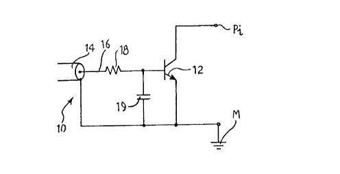
In all embodiments depicted in Figures 2 through 5, the basic component of probe10 is a transistor 12, which preferably is an n-p-n bipolar l,ansistor in the solutions shown
in Figures 2 and 4 (relating to a probe which allows forcing the respective point Pi to
ground voltage M) and is a p-n-p bipolar transistor in the solutions shown in Figures 3 and
5 (relating to a probe which allows forcing the respective fault point Pi to a fixed, positive
reference voltage +Vcc)
2~ In practice, in all embodiments shown, the collector of transistor 12 corresponds to
the terminal of probe 10 meant to be permanently or temporarily connected to the fault
insertion point Pi. The emitter of transistor 12, on the other hand, corresponds to the
terminal of the probe meant to be connected, here too permanently or temporarily! to the
pre-set signal level. The same ccnnection configuration can also be adopted for ECL logic
~n circuits, operating between 0 V ~ground M) and -5 V (-Vcc), by connecting the emitter o~
transistor 12 to voltage -Vcc (Figures 2 and 4) and to ground voltage M (Figures 3 and
5), respectively. In more general terms, :he solutions using an n-p-n transistor (Figures
2 and 4) allow forcing point Pi, connected to the transistor collector, to the lower one of
the reference voltage levels, i.e. M (typically 0 Volts~ or -Vcc (e.g. -5V). The solution witn
p-n-p transistor (Figures 3 and 5) allows instead to force point Pi to the higher reference
CA 0224831~ 1998-09-04
WO 97/33180 5 PCTIEP97/01096
voltage level, i.e. +Vcc or M, respectively.
In the diagrams of Figs. 2 and ~, probe 10 is connected to control device 1 for
instance by means of a coaxial cable of which shield t4 is connected to the reference
voltage (ground M or power supply voltage +Vcc), and hence to the emitter of transistor
12, and internal conductor 16 is connected to the base of transistor 12 through a bias
resistor 18 whose resistance is, for example, of the order or 100 Ohm.
~y the arrangement described, when transistor 12 is in cut-off condition the emitter
and collector terminals can be seen as electrically insulated from each other, so that probe
10, even if it is connected to the fault insertion point (Pi), actually has no impact on
equipment A (except for the considerations that follow). Tne manner for obtaining the cut-
off condition are well known. When transistor 12 is brought to a saturation condition - in
an equally known manner - tne transistor will behave as a short circuit between the
collector and emitter terminals. Point Pi is actually connected to ground level (Figures 2
and 4) or to power supply voltage Vcc (Figures 3 and 5). Under these conditions, the
1~ required fault insertion is accomplished.
The solutions shown in Figures 4 and 5 differ from the solutions shown in Figures
? and 3, respectively, because of the presence of a resistor 20 whose resistance is, for
example, of the order of one Ohm. Resistor 20 is preferably connected in series with the
emitter of transistor 12. Thus ths current flowing in transistor 12 (between collector and
emitter) when transistor 12 is in saturation condition, i.e. when the failure insertion is being
performed, passes through resistor 20. The voltage across resistor 20 is a signal represen-
tative of the value of that current, which signal can be sent back towards device 1 through
a feedback line, also comprising for example a coaxial cable with a shield 21 (usually
connected electrically via 22 to shield 14 of the cable driving the base of transistor 12)
2~ and an internal conductor 23 connected to the emitter of transistor 12. As a consequence,
cable 21, 23 carries a signal which is representative of current absorption in corresponden-
ce with fault insertion point Pi, thus allowing indications to be obtained on the electrical
load induced on equipment A by the fault insertion.
The behaviour just described in order to illustrate the general operating principles
3~) of probe 10 according to the invention constitutes an ideal model which fails to take into
account the presence of the parasitic capacitance (CCB) between collector and base of
transistor 12. Due to the existenca of that capacitance, whose value is of the order of one
picofarad (pF), the presence o, probe 10 connected to point Pi is not fully without
influence, particularly when fault insertion is not being performed.
To understand this, reference is made to the diagram in Figure 2 (the situation is
CA 0224831~ 1998-09-04
W O 97~3180 6 PCT~EP97/01096
identical for the diagram in Figure 4 and complementary for the diagrams in Figures 3 and
5).
Under norrnal operating conditions of the equipment, i.e. when fault insertion is not
being performed, the level o~ point ~i varies depending on the behaviour of the signals
which are present at that point (generally, binary signals). By way of example, point Pi will
switch between ground level M (logic "~") and level Vcc (logic "1"). In correspondence with
the rising edges of the signal present on point Pi, the oarasitic capacitance present
between the collector and the base of transistor 12 tends to create such an electrical
coupling between those terminals as to bring, at least for a brief instant, the base of
transistor 12 to a level sufficient to make the base-emitte r junction conduct. Consequently,
there is a current flow through the collector and the emitter of transistor 12 iiself. This
results, in practice, into a rather "distorted" rising edge, that is voltage on point Pi does
not grow steeply (st2p voltage) but rather with a more or less rounded edge influenced
by the conduction phase ind~ced into transistor 12.
The behaviour in the case of Figure a is wholly similar. In the solutions depicted in
rigures 3 and 5, on the other hand, a similar phenomenon affects the falling edges. In
this case as well, the parasitic capacitive coupiing between the collector and the base of
transistor 12 is such as to make, at least for a brief interval, the emitter-base junction
conduct. Thus transistor 12, at least temporarily, conducts and thus, again, "distorts" the
aforesaid falling edges.
To o~viate the aforesaid drawback, according to the invention a capacitor 19 is
directly connected between the base and the emitter of transistor 12, said cara :itor having
a capacitance value generally higher, preferably by at least two orders of magnitude
(hence a capacitance, for example, of 100 pF) than the parasitic capacitance existing
2~ between the collector and the base.
As shown by Applicant's experiments, and as can also be ascertained analytically,
the presence of c~p~citQr 19 is such as to contrast (and, for practical purposes, to cancel
out) the tracking of the collector of l~ansi~tor 12 by the transistor base due to the parasitic
capacitive coupling existing between those terminals.
In practice, thanks to the presence of capacitor 19 (a choice that goes against the
conventional desian rules for transistor circuits), probe 10 does not appreciably disturb
equipment A, while performing, very precisely and reliably, failure insertion at local level
(thus avoiding the typical drawbacks of those solutions which entail a sort of "transfer" of
point Pi to the outside through lonaer or shorter conductors).
CA 0224831~ 1998-09-04
The probe according to the invention is preferably manufactured as depicted
schematically in Figure 6.
The body of probe 10, comprising circuit elements 12, 18, 19 (and, in the case of
the embodiment shown in Figures 4 and 5, resistor 20), is preferably made as a
s miniaturised circuit, for instance with SMD (Surface Mounting Device) technology. The
probe body thus appears as a small container, usually dipped in resin, whose size is of
the order of a few millimetres. Two terminals 120, 121, corresponding to the emitter and
to the collector of transistor 12, come out from the container and are meant for connection
to board C in the way described above.
Figure 6 (which specifically refers to the embodiment depicted .in Figures 4 and 5)
shows the shields of two coaxial cables for connection to device 1, which cables are
equipped with respective connectors 140, 210 at the end remote from the probe body.
Obviously, in the embodiment shown in Figures 2 and 3 only one cable is present. Using
coaxial connection cables is advantageous for the purpose of exactly maintaining the
signal waveforms, especially with regard to absorbed current monitoring (resistor 20 and
cable 21, 23).
~ , " ,, . .: