Note: Descriptions are shown in the official language in which they were submitted.
S CA 02248507 1998-09-30
,
- 1 -
DIRECT SEQUENCE SPREAD SPECTRUM MODULATED UPLINK
FOR MODULATED BACKSCATTER ~Y~ IS
q~e~l Applications
This application is related to commonly ~ nPA U.S. Patent
5 Applic~tion~ Ser. No. 08r77s694, filed December 31, 1996, entitled "QPSK
tP.d B ML~C~ g System" and Ser. No. 08/571004, filed December 12,
1995, entitled "F.nh~nce~ Uplink Mo~ tPA R~L ~C~t~ ~ System."
Field of the Invention
This invention relates to wireless commlmi~ation systems and, more
10 particularly, to using direct sequence spread spectrum mo~lul~tion of subcatTier
frequencies in a mo~ PA b~rk~c~ttP,~ comm~)nic~tion system.
Back~round Of the Invention
Radio Prequency T~lf n~ ;on (RPID) systems are used for
i-lPntific~tion and/or tracking of c~luiplnf nt, in~,_n~ /, or living things. RPID
15 systems are radio commllniça~ion systems that communicate ~I~._cn a radio
transceiver, called an Interrogator, and a number of i~ ~n;,;~, devices called Tags.
The obj~;li~es of RFID systems are to design a reliable and secure ~h;t, ~ " andto minimi7P the total cost of the In~lug~tol and the Tags, while m~ting the system
~.çullllance ,~uil~-..e~.t~. In RFID systems, the Int~.lugalol comml)niç?t~-s to the
20 Tags using mo~ teA radio signals, and the Tags ~spond with mo~ la~ed radio
signals. The Interrogator first tr~n~mit~ an amplitude mod~ t~PA signal to the Tag.
Then, the Il~t~llugalur transmits a Corltin-lous-Wave (CW) radio signal to the Tag.
The CW radio signal can be a Fl~uency Hopping (FH) carrier, thereby Pnhqncing
the Tag's ability to operate in a multipath environments. The Tag then mo~vl~tp~s
25 the CW signal using Modvl~tP~1 Rac~ cattPring (MBS) where the ~ntennq is
electrically swilched, by the Tag's mo~vl~ting signal, from being an absorber of RF
r~ tion to being a reflector of RF radi~ti~n; thereby en~o~1ing the Tag's inform~ti~n
onto the CW radio signal. The Interrogator demodvl~tes the inSQming mo~vl~ted
radio signal and decodes the Tag's information mess?gp~ MBS systems typically
30 utilize amplitude mod~ ted techniques for commnni~tiQn~ from the Int~llùgator to
the Tag (downlink). For Tag to Interrogator (uplink) commnnil~ti~ns~ prior art
m~int~ins the use of na~row band modul~tion techniques fûr uplink comm~mic~tion~Prior art also m~int~in~ baseband homodyne detectiQn of the MBS signal at the
. CA 02248507 1998-09-30
Interrogator. To increase the probability of ~uccessrul data tr~n~mi~siQn, the Tag
may modulate the reflection coefficient at a rate higher than that of the data rate
thereby pro~-)cing a mod~ ted subcarrier signal on top of the CW RF signal.
In theory, subca~ r mo~ul~tion has the inherent advantage that the
S received wa~,efol~n, after mixing with the CW RF signal, produces a signal above the
DC noise of the homodyne detector, and away from the phase noise of the CW localoscillator. However, many objects local either to the Tag or the b~sest~tion will
reflect the CW RF signal back to the b~est~ti--n's l~ceh~r, and in the case where
moving rn~~hinery is present, MBS background noise at subca lier L~uencics up to10 a few megahertz are prod~lce-3 Moving m~chinery may inehlde: motors, ~nc~a~l~,
pumps, and fans. These m~- hines are common to industrial envil~ ...cr~t~ such as a
factory floor. Moving m~t~llic devices will modulate an incident RF wave at a
L~uency related to the rotation or vibration of the machinc.
Prior art has also used Direct Sequence Spreading of the CW radio
15 signal tr~fi~...ilt~ by the Inte.lul;~tcil, however, many MBS noise gen~alcn~ will
modulate the spread CW radio signal, which will be de~ ' by the ~t CIO~, and
will be lecei~,ed as MBS noise as in the nallù~ bàl d case, by the homodyne d~ or.
The.~ifol~, neither rl~uency Hopping nor Direct Sequence Spreading of the CW
radio signal offer advantages over MBS background noise.
20 Summary of the Invention
An embo~Nm~nt of the present invention provides an MBS system with
a pl~lcessing gain over MBS background noise by using a wi~b~n~1 uplin~ signal
and a n~luwl,and downlink signal where a narrowband signal is a non-spread
S~.,l~ulll signal. The wideb~n~ uplink signal is gene.at~d by controlling the
25 refl~ti~ of a nallu~ band downlink signal using a wi-leb~r~l data signal. Thewi-le~ data signal is generated by mQd~ ting a pseudo random signal with an
illÇo~ ;nn or data signal, where the chip rate of the pseudo random signal is higher
than the data rate of the data signal and where the data rate may be, for example, a
bit rate or a symbol rate.
An embo~1imen~ of the present invention illl~lO.~S packet capture when
multiple Tags simul~eously access an uplink time slot of a TDMA (Time Division
Multiple Access) system by Direct Sequence Spreading of the uplink signal. In a
Direct Sequence Spread Specl.u.,. TDMA system, the probability that two Tags
~ccessin~ the same time slot will have the same chip phase is small (or il~t. nlinnDlly
35 ~le~ to be small), the.~;f(j.~ a correlator receiver tracking one chip phase can still
demodulate one uplink burst if multiple Tags access a single TDMA slot.
~ CA 02248507 1998-09-30
In accor~ ce with the present invention, a duplex radio comm.lnir~tion
system comprises an Interrogator which generates a first mo~ulLqted signal by
modlllq-ting a first information signal onto a radio carrier signal. The Interrogator
trqn~mit~ the first mo~ ted signal to at least one remote Tag of the system. The5 remote Tag l~xe;~es and p~cesses the received first modlllqt~A signal. The Tag~nclaLcs a Pseudo-random Noise (PN) subcallicr signal, and in one embodiment,
Phase Shift Key modlllqtes a second information signal onto this subc~ thereby
generating a pseudo random subc~lier signal. The modlllqtion method can be either
amplitude, r1~UC n C~/~ or phase modlllq-tion of any cc , l~Yity; or a hybrid
10 combinq-tion of amplitude, fi~uency and/or phase modlllqtir~n A R- ~ L .~C~
Modulq-t~r using this pseudo random subca~ r signal mo~llllqtes the refl~ction of the
first mod~llqted signal, the reflected signal being a second m~ul~t~l signal. Itshould be noted that the pseudo random subcallier signal may also be used to
modlllqt~ a reflection of the unmodulq~ CW radio signal. The Intc~logatoll ~i;~S15 and demo~ es the second mo~ t~1 signal to obtain the second information
signal. In one embollim~nt~ ~...~]~lqtinn utili~s a ho.llodyn,t ~l~teclor and the first
modll1qt~ signal as the local oscill~r source for ~e homodyne d~P~I''.. The
Interrogator mixes the inco~it~g mo~lul~ted ~à~lerOllll with the local source
prod~lcing both In-phase and Qll~ 1rqtllre pseudo random subcarrier signals which are
20 bqn~lpq~s filtered at the subc~.;cr L~ucnc~, and input to a digital demodulqt~r. The
digital demo~ qtnr reproduces the second infollllation signal modll1qt~ by the
pseudo random subca- . ;P r L~UPnC~. The present in~n~n allows a MBS
applirqtion to operate in an en~holmlent where MBS bac~.>und noise is present,
i.e., an in~ ri~l or military envil~.l...c~-t The present invention also allows
25 multiple Tags in a Direct 5e~uence Spread S ~C~ n1 TDMA system, using an
Inte,,u~ with m~lltiFl~ N co~relator leeeh,el~, each tracking onc chip phase, to~."o~19t~ N Tags ~çces~in~ a single TDMA slo~
Brief Description of the ~ a~. ;..~!,
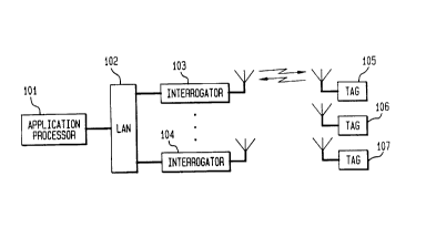
FIG. 1 is a block diagram of an illu~lla~ e Radio rl~ue
30 Tt1Pnl;t;r~;t)n (R~;ID) system;
FIG. 2 is a block diagram of an illu~llaLi~e Int~.~ugalor Unit used in the
R~ID system of FIG. l;
FIG. 3 is a block ~ ~m of a Tag Unit used in the RFID system of FIG.
l;
CA 02248507 1998-09-30
FIG. 4A is a logical diagram of a Tag Unit ~ tor Control of FIG. 3;
FIG. 4B is a logical diagram illustrating mixing a motl~ tP-l pseudo
random sub~ ;er with another subc&~l;e.,
FIG. S is a logical diagram of an In~,logalor Unit Pseudo Random
S Noise Sub~ ;crDemod~ t rUnitFIG. 2;
FIG. 6 is a logical diagram of a Demod~ tor Unit Time Acquisition
Unit of FIG. 5;
FIG. 7 is a logical diagram of a Dema~ r Unit Time Tracking Unit
of FIG. 5; and
FIG. 8 is a logic diagram of a Gate Array R~-eb -d DBPSK receiver
Unit of FIG. 5.
DePi'~d Description
One class of RFID applin~tionc involves using RFID tP~hnology to read
inf~nn~ti~n ~om a Tag affixed to a sensor, conlAine., rack, pallet, or object. In one
15 applir~tiQn the col~lAine- is moved across the ~~ 1ing field of an Il~t~lug~l. The
reading field is defined as that volume of space within which s~ccessrul
communir~tion~ . ~n the Tag and thc InteIrogator can take place. While the Tag
is in the reading field, the Interrogator and Tag must complete their information
eYch~nge before the Tag moves out of the In~,loga~ion field.
20 - With leÇe.ence to FIG. 1, there is shown an overall block ~lia~m of an
illusLla~ RFID system useful for describing the applir~inn of the present
invention. An Applir~tion ~ocessor 101 communir~tes over Local Area Netw~lk
(LAN) 102 to a plurality of In~,loga~ 103-104. The Intenogators may then each
communicate with one or more of the Tags 105-107. For e~-~..pk the Int~ llugalor25 103 ~ ,s an information signal, typically from an ~pplic~ n ~)cessor 101.
The InaL.~JDd~l 103 takes this inform~tion signal and ~ùcessol 200 (FIG. 2)
formats a downlin~ messagç (Information Signal 200a) to be sent to the Tag. Withjoint ~f~ncc to FIGS. 1 and 2, Radio Signal Source 201 gel ~,.dtes a radio signal,
the l~od~ tor 202 mo l~ ~s the Information Signal 200a onto the radio signal, and
30 the Tr~ 203 sends this modlll~t~ signal via Antenna 204, illu;~lla~i~,ely using
amplitude mo~ tion, to a Tag; however, other types of mod~ tion may be used,
for example, r~uen~;y and/or phase mod~ tion The reason for using amplitude
modlll~tion is that the Tag can demodulate such a signal with a single, ifi~ i./e
nonline~r device (such as a diode).
CA 02248S07 1998-09-30
In the Tag 105 (see PIG. 3), the Antenna 301 (for example, a loop or
patch ,qn~nna) lecei~es the mo~ te~l signal. This signal is demo~ q-te~l, directly to
baseband, using the Det~lol/~l.lqt~r 302, which, illustratively, could be a single
Schottky diode. The diode should be appropriately biased with the proper cuIrentS level in order to match the impe lqnce of the diode and the Antenna 301 such that
losses of the radio signal are minimi7~1 The result of the diode detector is
essenti-q-lly a demodulation of the il~co...ing signal directly to b~eb~n~ The
Information Signal 200a is then amplified, by Amplifier 303, and s~llcl~u.~i7q-tiQn is
l~co~el~d in Clock and Prame Recovery Circuit 304. The res~llting infonnatir n is
10 sent to a P~ocessol 305. The ~ucessor 305 is typically an i~ n~;~/e 4- or 8-bit
micloplocess~l, the Clock Recovery Circuit 304 can be implc~ n~ in an ASIC
(Applied Specific In~ated Circuit) which works to~lh.,. with ~1cessol 305 or it
be imple ..ent~ in ~ocessor 305's software program. The P~ùcessol 305 g~ne.at~s
an Information Signal 306 to be sent from the Tag 105 back to the In~.lu~lor (e.g.,
15 103). Information Signal 306 is sent to a l~o~lqtor Control Circuit 307 by
pl~lcessol 305 using timing infollllation genc.at~,d by clock and frame l~CU.e,~circuit 304. In an embo~i...P-nt using a TDMA time slot uplink p~locol, processor
305 uses clock, frame and time slot infonnq-fion from l~CO._. ~ circuit 304 to ensure
that the protocol's frame, time slot and guard time ~Uil~ mPnls are ~qti~fi.-
~
~ oc8ssor 305 may use interaction fmm the l.,co~ d information signal 200a to
llh~e which frame (or frames) and which time slot (or slots) within a frameshould be used to send information signal 306 to the In~.lùgalol. Mofllllqt~r controlcircuit 307 uses Infonnqtic-n Signal 306 to modulate a p~udo random noi~
subc~lier ~n~.~d by the Mo~ q-tnr Control Circuit 307 and driven by r~uency
25 Source 308 to produce signal 311. The rl~uc.,~;~ Source 308 may be a crystal
oscillq-tor ~parate from the ~cessor 305, or it may be a Çlcquen.;y source derived
from signals present inside the P~ucessor 305 - such as a divisor of the primary clock
rl~uen~;~ of the ~ocessor which is obtained from o~~ q-t~r 312. The modlllqt~d
Pseudolandc~,,. su~z~.;e- Signal 311 is usedbyDe~ o~llllq~r3o2to
30 m~lllqtP the radio carrier signal ~~,ce;vtd from In~ lugator 103 to produce amod..lq-tçd b-~L!~c~ (e.g., l~,llect~l) signal. This is ~rco~ )lish~ by s~ilchillg on
and off the Schottky diode using the Pseudo random sulx~- ~ ;f r Signal 311, thereby
~hAnging the re~ec!A~-ce of Antenna 301. A Battery 310 or other power supply
provides power to the cu~;uill~ of Tag 105.
CA 02248507 1998-09-30
Mc~ n~ion
There are a variety of techniques for using MBS to send inf~m~ti-n
from the Tag to the Intellùgator. In some MBS technologies, the Modul.,t~r Control
Circuit 307 of the Tag ~n~,.ates an amplitude mo~l-llq-tP~ signal by modnlq-ting a CW
5 signal received from the Interrogator with an Information Signal 306 having a
frequencyf2. If the Radio Signal Source 201 gCll~,~ateS a CW L~ucn~;yfc, then the
Interrogator receives signals from the Tag atfc whose bandwidth is 2f2 and filters
signals outside of this bandwidth range. This a~luach could be termed the "MBS at
bqcebqnd" app~ach.
Another approach would be for the Tag to g_nc,~alt a subc~uli~,,
frequencyfS, e~ ~ t~'fi by r.~uen.;~ Source 308, as shown in FIG. 3. The
information could be con.e~od using AM (~mplitl)dp~ ~odlllq~ion)~ FSK (I ~u~n -~y
Shift Keying) or PSK (Phase Shift Keying) by mo~lllqting the subc~ f s with the
Information Signal 306 having a rl~ucrl.;~f2 tocreate signal 311. In this e~ le,
15 the Interrogator l~,C~ .S signals atfc~ whose bandwidth is 2f2 but at a Ll~uc~ fs
away fromfc. This method is termed "MBS of a subcdll;cr." Here we use the
al)plù~ch of g~nc.a~il-g a pseudo random noise subcall;e,r 402, at chip ratef5, whose
bandwidth is 2f5.
When the Tag 105 detects the ~ SenCe of the Interrogator downlin
20 signal, it respondc by ~ c~ -g its RFID data pl~ by a known preamble that
is used for ~llc}~o~ t;on by thc l~,ce;~,el. In one embod~ c~, and in l~fc.~;. ce to
FIG. 4A, the Tag sends an uplink message to the Interrogator by dirr~ ially
enl~oding the uplink data inforrnation signal 306 at rl~ucn ~f2 and BPSK
modulates a pseudo random signal 402 to gcnc~dlor signal 311. The pseudo random
25 signal is gene~ratpd by a maximum length shift register 401, which is cloc~P~ at
rl~ucn~,~f5 obt ~ from signal source 308. The resulting pseudo r~ndom
subcaIrier Signal 311 is used by Dc,~clol/Modulator 302 to mo~ t~ the radio
carricr signal l~ce;~c,d from Int~.lug~or 103 to produce a modul~tP~ ~L~C~
(e.g., lcne~t~:l) signal at the rate of the basestation ~ecei~ des~ 1in~ code rate
30 (f5); thereby s~Pn-ling a second mod~ ted signal back to the Int~ ùgalor. The Tag
should have a prior knowledge of the desp,ea~ g code and rate; in one embodimentthis can info m~tion can be tr~ncmittPA by the inform~tion signal 200a. For
example, information signal 200a may specify one of several de~ - ling or
spreading codes to be used on subsequent co~ lnic~tions ~I-.~n the Tag and the
3S Interrogator.
~ CA 02248507 1998-09-30
In another embo-1imp~nt and in ~efe.~llce to FIG. 4B, the Tag ge.1e.~tes a
subc~lier frequencyf5, and mixes the mod~ ted pseudo random subc&.~ signal
311 vith sub~,~l;er f 5, thereby producing a mod~ t~A pseudo random noise
subc~l;er signal. The result of this mixing is used to control the reflectivity of the
S de te~lol mo~ tor 302, thereby sending a second mc~ tPA signal back to the
Interrogator.
Rec~ r
Returning to FIG. 2, the Interrogator 103 l~ce.~.cs the reflected and
mo~ul~tPA. signal vith the Receive Antenna 206, amplifies the signal with a Low
10 Noise ~mrlifier 207, and demo~ul~tp~s the signal using ho.llol~..e detP,ction in a
Mixer 208 down to the Inte.-..P l;~tp~ Frequency (I~) of the single subc~ f5. (In
some Inte.l~gaLor desi~, a single Tl~n~n;l~ r 204 and Reccive 206 Antenna is
used. In this event, an elccL.ollic method of separating thc t.~ ~ signal from
that received by the receiver chain is need~1; this could be n,, ccmpli~heA~ by a device
15 such as a Cinculator.) Using the same Radio Signal Source 201 as used in the
chain means thc demod~ tion to IF is done using T~omoflyne ~ete-ction; this
has advantages in that it greatly reduces phase noise in the receiver circuits. It
should be noted that mod~ tP,d signal 215 may be used by Quadrature Mixer 208 todemodulate the signal from amplifiPr 207 using ~nm~yne detection. Thc Mixer
20 208 then sends a Down Converted Signal 209 -- if using a Ql -~tvre Mixer, it sends
both I (in phase) and Q (quadrature) signals -- into Filter/~mp!ifier 210 to filter and
hard limit the Demo~ul~tPd Signal 209. The nesultin~ filtered signal -- then typically
an Information Signal 211 carried on an IF suhc~- . ;er -- is then dpms)dll1~tp~ from
the subcalli~ in the S~ Demodlll~tQr 212, which then sends the Information
25 Signal 213 to E' ocesso. 200 to d~ --;nr the content of the ...essage. The I and Q
ch~nn~lc of Signal 209 can be combimP~1 in the Filter/~mplifi~r 210, or in the
Subcanier ~emodul~t~r 212, or they could be combined in the ~ OCCSSOl 200.
For this lece;~er confignration any MBS background noise signals will
not be dcspl~-1 by 212 and passed along to the pl~)cessor 200. Th~îol~, only
30 desired signals arriving at the receiver, mo~ tP~ by pseudo random noise code at
ratefS, will be despread and passed along to the p.~)cess~. 200. Any na..owband
signal will be spread in frequency and passed into the plOCeSSOI 200 as additiven noise. Thus, the desired MBS signal 213 will have the advantage of a
pç~cessi.-g gain over MBS background noise.
CA 02248507 1998-09-30
There are several choices for imple.nen~i.lg the data leco~,y in
subc~ ;er demodulator 212: conventiQn~l analog VQ demo~ tion and envelope
detectior. of the pseudo random subcarrier signal using, e.g., a Costas Loop, Digital
Signal Processing (DSP) of the sampled subcarrier, or implementing a receiver in5 digital logic.
Dem~ls~ion
The demodlll~tor 212 may be implem~nte l in Gate Array circuit,
illu~Llali~cly shown in F~G. 5. It has three filn~tion~:
1) despl~,ad the in~o-..;--g direct se~luence spread ~ U111 il~Co~
10 signal;
2) demod~ tion of the dirr~ ially e ~~od~ phase shift keyed data
(data leco~ circuit);
3) deriving the received bit clock for the dem~ tP~ data stream (clock
recovery circuit).
Timing recovery of the pseudo random ~lvence chip code is pelr,l.l.cd
in two stages: Timing acquisition and time trackin~ The timing acquisition circuit
finds where the tr~n~mittPr is in the PN code ~uence Once the l~cG;~r has PN
code lock, it ac.lu l.,s bit synch. Once bit synch has been achie~c,d, the l~cei~.er then
acquires "word" synch, meaning the packet boun(l~ri~s are found and ~he.~,ro~ the
20 m~ning of each byte in the packet may be decod~d The packet bol~n(l~ries are
defined by the first thil ~n bits being a known s~uel ce (e.g., a barker codeword)
and the last two bytes being a CRC che~L ~u~... Time t~~L ing iS the fine adju~ e--
~of the .~ce;~ pseudo random code sequence gen.,.aLor to m~int~in lock with the
tr~n~mitting pseudo ., ndo... code sequence ~ne~tor.
The input to the data l~co~ e-mod, t~r circuit 212 is a har~ limited
subc~ ,r 211, which in one embod;...f,nt is modul~t~ by ~iirL,.~,.,.ially çnrod~d
BPSK and spread by a ma,~h..ul.. length pseudo random bit sequence at chip rate f 5.
The su~ . is input to both the timing acquisition unit 501 and the time trackingunit 503. The time acquisition unit 501 is used to find a rough estim~ of the
30 present chip code sequence used to spread the subc-~ . ;P r 211. When the time
acquisition unit finds the current chip phase of the subc~ . ;e- 211 , it alerts the time
tracking unit 503 by asserting the Lock signal 502. When the time tracking unit 503
ece;~.es the Lock signal 502, it de;,~ ds the in~o~ing subc~ . 211 and produces
the differentially encodçd BPSK infonn~t~ signal 504, which is an cstim~t~ of
35 inform~tion signal 306. The di~nLially encode BPSK signal 50~L is passed to the
CA 02248507 1998-09-30
Ra~eb~nd Demod~ tor Unit 505 which di~.en~-ally decodes signal 504 and
g~,n.,.at~,s the inf~rm~tion signal 213.
In l~,fc.~nce to FIG. 6, the time acquisition unit 501 lcCCh,eS hard
limited subc~li~,r 211 and ~alllp1es N chips at frequency ratef5, which are serially
S shifted into register 601. A locally genc.atcd maximum length pseudo r~n-lom code
sequence is ge.ll~d~d in register 603 and col.-p~cd to the data stored in register 601.
If a match is dPtected, then Lock Signal 502 is asserted. If no match is detected, then
a new value is generated in register 603. In one embo.1;...c.l-, to achieve dming
acquisidon a scp~alc correlator ~~ce;-_r section that Op~atCS many times faster than
10 ~ l; ng chip rate, using a local pseudo random code se~ e nce generator running
at the master clock rate is used to search and find the pseudo random code phase of
the current input data stream. For ex~mple, the master clock may run well above
100 MHz. In one embo~ ..e ~ the subca.li~.r demod~ r or baseband l~Cc;-C~iS
imple...cn~P~ using a FPGA (Field Programmable Gate Array) and, as a result, the15 correlator receiver se~l;ons operadonal speed is limited by the FPGA's ma~l-ulll
5peC;r;cd clock rate. The dming ~lui~ilion circuit only needs to mnnit~ the codesymbols used for the prcamble bits of the uplink ~e5s~g~ If timing acquisidon isnot achieved by the end of the messag~ preamble bits, the ...csc~ cannot be
p~pe.l~ el~o(le~l and will be l~ijcc~l by the ,ccei~,.'s digital logic. The use of a
20 preamble word is to allow a sllffirient number of bits to pass through the l~ce;-_l to
allow the timing recovery CilCuil~r to acquire PN code synch and bit timing synch.
In this implemen~tinn the I~Ce;-~,l iS not looking to find the p~eamble data. If the
CCe;-~- âC~Iuil~,S synch it will look for the beginning of mess~gç code word, usually
a barker s~ucncc. If the receiver finds the mq-t~ l~ing barker word, then it d~o~es
25 the rest of the packet, defining the m~qning of the packet bits and bytes by their
offset ~ cl-ir to the end of the barker word. At the same dme the l~ce;~..,. iS
cqlc )~tir~g a CRC çl-~ ... over the .~ei~l packet bits and CO-II~&~S the result to
the last t~vo bytes in the packet, which are the ~ ..;l~ CRC cl~L ~-... If they
match, the packet is ~c~ to have been l~,cei-~,d ccnl~~
In one impl~l.. ent~l;Qn, the ba~eb~n~ digital demodnlqt~r, including data
timing ~co.e.~, operate from a 4 MHz clock osç~ qtQr driving the master clock ofthe FPGA. All other clocks and timing inside the FPGA are derived from the master
clock. The master clock rate is 80 times greater than the bq~eb~n~ data rate of 50
Kb/s.
In l~fe.~nce to FIG. 7, the Time Tracking Unit 503, after ~ce;ving Lock
Signal 502, uses an Early-Late tracking scheme to demodulate the subc~-Iiel 211. In
one emW;...I -t the dme acquisition circuit 501 loads the state of maximum length
CA 02248S07 1998-09-30
- 10-
pseudo l~uldol~ register 603 into the dme tracking maXimum length shift register 701
(these could physically be the same register inside a Gate Array). The incoming
subcarrier 211 is muldplied by three dirr.,.~nt dme delayed ~ ions of the N chipmaximum length shift register 701: a late dme version 705a, an early time version
5 705b and the present dme estimAte version 705. The three results 706a, 706b, and
706 are input to three correlator match filter d~ t. c~ 702. The correlator match
filter detectors 702 integrate/accumulate, over N s~"~'es, the reslllting
autocorreladon between the subca"i~. signal 211 and the input dme delayed samples
of N chips from m~ximum length shift register 701. The coll~lat~i de br~lo~ 702
10 having the maximum output reslllting from the three inputs 706a, 706b and 706 is
d~te.",ine,d to be the correct dme reference for the inro~;ng subc - . ;e~ signal 211.
The Timing Circuit 703 adjusts the clock ,~ifc.~nces 704 and 510 of registers 701 and
603"~p~;lively to m~intAin chip lock with the il-co~ing subcarrier signal 211.
In ,~fe.~nce to FIG. 8, the output ~eric;on of the correlator match filters
15 is the dirr~ ially e.~-codcd BPSK informadon signal 504, which is a baseband
signal at informadon rate f2. It is Low Pass Filtered in filter 801 and the output 804
is input to a digital phase lock loop circuit 806, which derives the receive clock for
the s~lbcz~ ~ ;e ~emofllll~tinn circuit 212. The baseband signal 804 is mnltirli~ by
muldplier 803 with a one bit delayed version 805 p~l~ ;.-g the ba~b~d
20 dçmo~lul~tr)r output signal 213.
In a Direct S~uc,nce Spread S~;llu l~ TDMA system, the pl,~p~ility
that two Tags ~ces~ing the same dme slot will have the same chip phase is small,,h~rO,~ a correlator l~cei~cr tracking one chip phase can still de-.-~ te one
uplink burst.
It should be noted that the pl-~cessi~-g gain provided may be
by:
PG = Bws/Bwd = N
where PG is the ~ )cGs~in~ gain, Bws is the bandwidth of the direct sequçnre spread
,u", su~-- . ;e- signal, Bwd is the bandwidth of the inro~ l;on or data signal,
30 and N is the number of chips per inform~tion or data bit.
We further note that a DQPSK (Dirr~ ial Quadrature Phase Shift
Keyed) suhcA. ~ ;P r demo~ulAtor has the same plopell~ as the DBPSK (Dirr~l~n~ial
Binary Phase Shift Keyed) subcallier demo~ At ~r shown in FIG. 4A, in the same
manner as above. Thus, e~ctenciQns to higher order M-order DPSK (Differential
35 Phase Shift Keyed) modul~tiQn sch~mes may be implr...P..t~
CA 02248507 1998-09-30
- 11 -
What has been described is merely illustrative of the application of the
principles of the present invention. Other atTange...P.nl~ and methods can be
i.nple...el-~ by those skilled in the art without departing from the spirit and scope
of the present invention.