Note: Descriptions are shown in the official language in which they were submitted.
, CA 022488~1 1998-10-02
Patent
97-178 CA
SPECIFICATION
MALE CONNECTOR FOR FLAT FLEXIBLE CIRCUIT
Field o~ the Invention
This invention generally relates to the art of
electrical connectors and, particularly, to connectors for
electrically interconnecting flat flexible circuitry.
Background of the Invention
A flat flexible circuit conventionally includes
an elongated ~1at flexible dielectric substrate having
laterally spaced strips of conductors on one or both sides
thereo~. The conductors may be covered with a thin,
flexible protective layer on one or both sides of the
circuit. If protective layers are used, openings are
formed therein to expose the underlying conductors at
desired contact locations where the conductors are to
engage the conductors o~ a complementary mating connecting
device which may be a second ~lat flexible circuit, a
printed circuit board or the terminals of a mating
connector.
A wide variety of connectors have been designed
over the years for terminating or interconnecting flat
flexible circuits with complementary mating connecting
devices. However, problems continue to plague such
connectors, particularly in the area of cost, complexity
and reliability. Not only is the direct material costs of
such connectors relatively high, but an undue amount o~
labor time is required in assembling such connectors.
Furthermore, each connector is designed and manufactured to
accommodate a particular flexible circuit size with a ~ixed
conductor spacing and therefore ~or each size ~1exible
circuit a single connector must be designed, manufactured
CA 022488~1 1998-10-02
Patent
97-178 CA
and inventoried. In addition, the cost and time associated
with application tooling for the connectors and their
~lexible circuits also adds to the problems associated with
such connectors. The present invention is directed to
solving these problems by providing simple, inexpensive and
reliable connector structures not hereto~ore available
Summary of the Invention
An object, there~ore, o~ the invention is to
provide a new and improved connector for ~lat ~lexible
circuitry.
Another object o~ the invention is to provide a
new and improved male connector ~or electrically
interconnecting the conductors o~ a ~lat flexible circuit
to the conductors o~ a complementary mating connecting
device.
In the exemplary embodiment o~ the invention, the
connector includes a male body member on which the flexible
circuit is positioned with the conductors o~ the circuit
~acing away from the body member. A yieldable backing
structure is disposed on the body member beneath the
~lexible circuit ~or resiliently biasing the conductors o~
the circuit against the conductors o~ the mating connecting
device when the connector is mated with the device.
As disclosed herein, the body member is molded o~
relatively rigid plastic material, and the yieldable
backing structure is o~ elastomeric material such as
silicone rubber. In one embodiment o~ the invention, the
yieldable backing structure is a molded-in-place component.
In another embodiment of the invention, the elastomeric
backing structure is separate ~rom the body member and
~ixed thereto. In still another embodiment o~ the
invention, the yieldable backing structure is integral with
CA 022488~1 1998-10-02
Patent
97-178 CA
the body member, such as an integrally molded spring
structure.
The invention contemplates that a single size
connector can accommodate a range o~ ~lex circuit conductor
designs within the same size ~lex circuit inasmuch as
individual terminals are eliminated. Furthermore, since
the connector does not use terminals, the costs and time
associated with application tooling is completely
eliminated.
Other objects, ~eatures and advantages o~ the
invention will be apparent ~rom the ~ollowing detailed
description taken in connection with the accompanying draw-
ings.
CA 022488~1 1998-10-02
Patent
97-178 CA
Brief Description of the Drawinqs
The features of this invention which are believed
to be novel are set forth with particularity in the append-
ed claims. The invention, together with its objects and
the advantages thereof, may be best understood by reference
to the following description taken in conjunction with the
accompanying drawings, in which like reference numerals
identify like elements in the figures and in which:
FIGURE 1 is a perspective view of a female
connector terminating a flat flexible circuit, according to
the invention, along with a printed circuit board mateable
with the connector;
FIGURE 2 is an exploded perspective view of the
female connector and flat flexible circuit;
FIGURE 3 is a view similar to that of Figure 2,
showing the yieldable backing structures as separate
components;
FIGURE 4 is a perspective view of the female
housing in a partially open condition;
FIGURE 5 is a view somewhat similar to that o~
Figure 2, but with the connector adapted for terminating a
double-sided flexible circuit;
FIGURE 6 is an exploded perspective view of the
connector of Figure 5, with the yieldable backing
structures shown as separate components;
FIGURE 7 is a perspective view of an alternate
embodiment of a female housing in a substantially open
condition;
FIGURE 8 is a perspective view of the female
housing o~ Figure 7 about to be closed and latched;
FIGURE 9 is an exploded perspective view of an
embodiment of the female connector adapted for mounting in
a panel;
CA 022488~1 1998-10-02
Patent
97-178 CA
FIGURE 10 is a perspective view of the connector
o~ Figure 9;
FIGURE 11 is a perspective view o~ a male
connector ~or terminating a flat ~lexible circuit,
according to one embodiment o~ the invention wherein the
yieldable backing member is a molded-in-place component;
FIGURE 12 is a perspective view o~ the connector
o~ Figure 11, with the ~lexible circuit terminated thereto;
FIGURE 13 is a view similar to that o~ Figure 12,
but with the latches o~ the connector o~ a di~erent
con~iguration;
FIGURE 14 is a view similar to that o~ Figure 11,
but with the yieldable backing structure being a separate
component;
FIGURE 15 is a view similar to that o~ Figure 14,
but with the male connector adapted as a double-sided
connector;
FIGURE 16 is a view similar to that o~ Figure 11,
but with an alternate means o~ providing a flexible circuit
strain relie~ by passing the ~lexible circuit through an
integrally molded slot;
FIGURE 17 is a view similar to that o~ Figure 16,
but with the yieldable backing structure being a plurality
o~ integrally molded spring ~ingers;
FIGURE 18 is a perspective view o~ still a
further embodiment o~ a male connector embodying a movable
cable clamp; and
FIGURE 19 is a perspective view o~ an embodiment
o~ a male connector similar to that o~ Figure 18 but with
a movable cable clamp incorporating a latching mechanism.
CA 022488~1 1998-10-02
Patent
97-178 CA
Detailed Description of the Preferred Embodiment
Referring to the drawings in greater detail, the
concepts of the invention are disclosed herein as embodied
in a connector assembly, including a female connector and
a male connector. Various embodiments of the female
connector are shown in Figures 1-10. Various embodiments
of the male connector are shown in Figures 11-18. It
should be understood that the female connector can be mated
with the male connector as a connector assembly, or either
the female connector or the male connector can be used
alone for electrically interconnecting the conductors of a
flat flexible circuit to the conductors of a variety of
other complementary mating connecting devices.
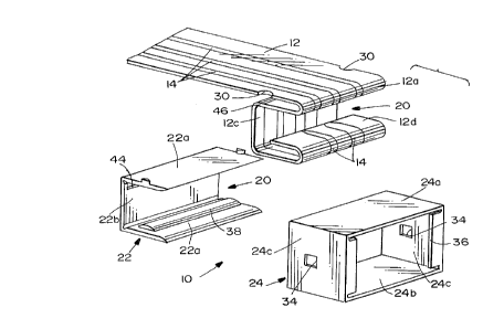
For instance, Figure 1 shows a female connector,
generally designated 10, for terminating a flat flexible
circuit 12 and electrically interconnecting the conductors
14 of the flexible circuit to conductors or circuit pads 16
on one or both sides of a rigid printed circuit board 18.
Figure 2 shows female connector 10 in conjunction
with the flat flexible circuit 12 which has been folded for
assembly purposes. For reference or nomenclature purposes,
the flexible circuit has been folded to include an upper
front fold 12a and a lower front fold 12b between which the
flexible circuit is folded into a generally U-shape to
define a rear fold 12c. This configuration defines a
mouth, generally designated 20. The distal end 12d of the
flexible circuit is folded in a rearward direction, as
shown.
Still referring to Figure 2, female connector 10
includes a female housing, generally designated 22, and a
box-like outer shell, generally designated 24. The female
housing is generally U-shaped and includes a pair of side
wall portions 22a defining opposite sides of a cavity,
generally designated 26, along with a rear wall portion 22b
CA 022488~1 1998-10-02
Patent
97-178 CA
which de~ines the rear o~ the cavity. The upper side wall
portion includes a pair o~ tabs 28 at opposite edges
thereo~ which seat into recesses 30 in opposite edges o~
~lexible circuit 12 for properly locating the circuit
relative to ~emale housing 22 and to provide strain relief
~or =the circuit. The female housing is a one-piece
structure integrally molded o~ dielectric material such as
plastic or the like. Side wall portions 22a are joined to
rear wall portion 22b by integrally molded living hinges 32
which permit the wall portions o~ the ~emale housing to be
movable between an open condition and a closed condition,
as described hereina~ter.
Rigid outer shell 24 (Fig. 2) o~ ~emale connector
10 also is a one-piece structure including top and bottom
walls 24a and 24b, respectively, and a pair o~ opposite
side walls 24c. The side walls are provided with latch
openings 34 ~or purposes described hereina~ter. The shell
has a ~ront opening 36 which is aligned with cavity 26 o~
female housing 22 when the connector is in assembled
condition as shown in Figure 1.
The invention contemplates that ~emale housing 22
be provided with a yieldable backing structure 38 on the
cavity-side o~ one or both o~ side wall portions 22a for
resiliently biasing conductors 14 o~ ~lexible circuit 12
received in cavity 26 against the conductors o~ the mating
connecting device (such as printed circuit board 18) when
the connector is mated with the device. With ~lexible
circuit 12 ~olded as shown in Figure 2, upper front ~old
12a will embrace top side wall portion 22a and lower front
~old 12b will embrace lower side wall portion 22a, so both
side wall portions will be provided with one of the
yieldable backing structures 38. It can be seen in Figure
2 that each yieldable backing structure is elongated in the
direction o~ the width o~ the ~lexible circuit so that the
CA 022488~1 1998-10-02
Patent
97-178 CA
backing structure is at least wide enough to resiliently
bias all o~ the conductors 14 of the circuit against their
respective conductors of the complementary mating
connecting device. It can further be seen that the backing
structure 38 is generally uniform in size and therefore can
resiliently bias a flex circuit having any conductor
configuration or thickness. That is to say, since there
are no discrete terminals in the connector, the layout of
the flex circuit and the positioning of the conductors
thereon is not critical to the actual connector or
connector size. Therefore, in applications such as high
current applications where the conductor thickness may be
larger than other, lower current applications, the
connector configurations can remain the same.
Figure 2 represents an embodiment o~ the
invention wherein the yieldable backing structures 38
comprise molded-in-place components, as described below.
Figure 3 represents an embodiment wherein yieldable backing
structure 38A are separately molded components secured in
place by tabs 40 inserted into holes 42 in side wall
portions 22a o~ the female housing. Adhesives may be used
to ~urther ~ix yieldable backing structures 38A in
position. Whereas female housing 22 is molded o~
relatively sti~~ or rigid plastic material, yieldable
backing structures 38 or 38A are molded or otherwise
fabricated o~ elastomeric material such as silicone rubber
or the like.
Figure 4 shows female housing 22 in a partially
open condition in comparison to the closed U-shaped
condition of Figure 2. In particular, side wall portions
22a can be moved or rotated relative to rear wall portion
22b about living hinges 32 until the entire female housing
is in a flat, fully open condition. In this condition,
yieldable backing structures 38 can be very easily
CA 022488~1 1998-10-02
Patent
97-178 CA
assembled or ~abricated to the side wall portions, i.e.
much easier than i~ the ~emale housing was a rigid closed
structure With the embodiment o~ Figure 3, yieldable
backing structures 38A simply are positioned on the open
side wall portions and ~ixed into place by way o~ heat
staking, latching, ultrasonically welding or the like. In
the embodiment o~ Figure 2, yieldable backing structures 38
can easily be molded-in-place in elongated recesses in the
side wall portions, with the side wall portions in their
open, ~lat condition. The invention contemplates that the
molded-in-place backing structures 38 can be insert molded
into the recesses in the side wall portions. On the other
hand, it is contemplated that the backing structures can be
molded in a "two-shot" ~abricating process wherein the
plastic material o~ the ~emale housing is injected in one
shot, the silicone rubber o~ backing structures 38 is
injected in a second shot, and the materials are cured
sequentially, i e., the plastic material is cured during
the second shot injection.
Figure 5 shows an embodiment very similar to that
o~ Figure 2, but an elongated slot 44 is ~ormed in rear
wall portion 22b o~ ~emale housing 22 immediately below top
side wall portion 22a. This slot enables the connector to
be used with a flat ~lexible circuit 12 which is "double-
sided" In other words, the circuit has conductors 14 on
both sides thereo~. In assembling the double-sided circuit
to ~emale housing 22 with slot 44, the circuit, as at 46,
pro~ects through slot 44 such that rear ~old 12c o~ the
circuit is disposed on the outside of rear wall portion 22b
o~ the ~emale housing. The ~lexible circuit then is ~olded
around the outside o~ the bottom side wall 22a until distal
end 12d of the circuit is disposed inside cavity 20 on top
o~ the lower yieldable backing structure 38. There~ore,
the conductors 14 on the underside o~ the circuit now ~ace
CA 022488~1 1998-10-02
Patent
97-178 CA
upwardly into the cavity, whereby the conductors on both
sides o~ the circuit are engageable with the conductors on
two sides o~ an appropriate complementary mating device.
In the double-sided embodiment o~ Figure 5,
yieldable backing structures 38 are molded-in-place
components, as described above. Figure 6 shows
substantially the same embodiment, but the yieldable
backing structures 38A are mechanically fixed and glued in
place as described above in relation to Figure 3.
Figures 7 and 8 show an alternate embodiment o~
a ~emale housing, generally designated 22A, which not only
has opposite side wall portions 22a and rear wall portion
22b, but the housing construction o~ Figure 7 includes a
pair o~ opposite end wall portions 22c. The end wall
portions are pivotally connected to the side wall portions
by living hinges 45. The side wall portions have hooked
latch arms 46 which latchingly engage within latch holes 48
in end wall portions 22c to hold the ~emale housing
construction in a closed box-like con~iguration. This
construction can be used to eliminate outer shell 24 Yet,
female housing 22A still can be ~ully opened to allow
yieldable backing structures 38 (or 38A) to be assembled or
molded-in-place on side wall portions 22a, wherea~ter the
structure can be closed to de~ine a cavity ~or receiving
the ~olded ~1exible circuit.
Figures 9 and 10 show an embodiment o~ a ~emale
connector, generally designated lOA, which is adapted ~or
mounting in an opening in a panel. Female housing 22 is
substantially identical to that described above. However,
shell 24A include ~1exible arms 50 and rigid arms 52 ~or
engaging opposite sides o~ a panel, with shell 24A and,
thereby, the connector lOA (Fig. 10) disposed in an opening
in the panel. O~ten, such panel-mounted connectors are
mounted in "blind mating" environments and, consequently,
CA 022488~1 1998-10-02
Patent
97-178 CA
flared flanges or lips 54 are provided about opening 36 in
the shell in alignment with cavity 26 in the female housing
thereby providing a self-aligning feature for a
complementary mating device such as a mating connector.
Figures 11 and 12 show a male connector,
generally designated 60, for electrically interconnecting
conductors 14 of flat flexible cable 12 to the conductors
of a complementary connecting device. For instance, the
male connector may have hooked latch arms 62 at opposite
ends thereof for latchingly engaging within latch openings
34 (Figs. 1 and 2) in side walls 24c of shell 24 of female
connector 10. The male connector would be properly sized
for insertion through front opening 36 in the shell and
into cavity 26 in female housing 22.
More particularly, male connector 60 has male
body member, generally designated 64, defining opposite
sides 64a and a front edge 64b. In the embodiment of
Figures 11 and 12, a yieldable backing structure 66 is
molded-in-place in a recess or indentation in one or both
opposite sides 64a of body member 64. Similar to female
housing 22 and yieldable backing structure 38 of female
connector 10, male body member 64 can be molded of
relatively rigid plastic material, and yieldable backing
structure(s) 66 can be molded of elastomeric material, such
as silicone rubber. The yieldable backing structure(s) can
be either insert molded on the male body member, or the
backing structure(s) and body member can be simultaneously
molded as a "two-shot" injection process as described
above.
In assembly of flexible circuit 12 to male
connector 60, the flexible circuit is folded around front
edge 64b of male body member 64 as shown in Figure 12, with
conductors 14 of the flexible circuit facing away from the
body member. Positioning holes 68 are provided in the
CA 022488~1 1998-10-02
Patent
97-178 C~
~lexible circuit ~or press-~itting engagement with bosses
70 on opposite sides o~ body member 64 to position and
provide strain relief ~or the ~lexible circuit wrapped
about the male body member. Yieldable backing structure(s)
66, thereby, lie beneath the ~lexible circuit ~or
resiliently biasing conductors 14 o~ the circuit against
the conductors o~ the mating connecting device when the
connector is mated with the device.
Figure 13 shows an alternate embodiment o~ a
~emale latch structure 72 at each opposite end o~ male
connector 60. These ~emale latch structures may latchingly
interengage with appropriate latches on a complementary
~emale connecting device. On the other hand, it can be
seen in Figure 13 that ~emale latches 72 are of~set
upwardly out o~ the plane o~ body member 64 to an extent
that latch arms 62 (Figs. 11 and 12) can be inserted
thereinto to enable two separate male connectors to be
intermated with the respective yielding backing structures
66 o~ the respective male connectors biasing the two
respective ~lexible circuits toward each other to
interengage their respective conductors
Figure 14 is similar to Figure 11, except that
the male connector includes yieldable backing structures
66A which are molded separately ~rom body member 64 and
subsequently positioned within recesses 74 in one or both
sides 64a o~ the body member. The yieldable backing
structure(s) can be a~ixed within recesses 74.
Figure 15 shows an embodiment of the male
connector wherein a single-sided ~lexible circuit is
terminated on both sides o~ the connector, that is, a
redundant contact con~iguration. Unlike the embodiments
shown in Figures 11 and 14, instead o~ wrapping around body
member 64, the ~lexible circuit 12 is inserted in the
direction o~ arrow "B" through slot 82 and beneath a top
, CA 022488~1 1998-10-02
.
Patent
97-178 CA
ledge 84. The ~lexible circuit then wraps around a
con~iguration o~ stacked yieldable structures 66, and exits
through a slot similar to 82 (not shown) on the bottom o~
body member 64. Each o~ the yieldable backing structures
66 is located in a recess 74 on opposite sides o~ an
integrally molded sunken wall 80 and may be separately
molded, as shown and as in Figure 14, or molded-in-place,
as in Figure 11.
Figure 16 shows an embodiment similar to that o~
Figure 15, but backing structure 66B is shown as a bar
molded unitarily with body member 64 o~ the male connector
and wall 80 is the yieldable structure that provides the
resilience ~or the relatively rigid backing structure that
there~ore allows the conductors o~ the ~lexible circuit to
be biased against their respective conductors o~ the
complementary mating connecting device.
Figure 17 shows an embodiment o~ a male connector
60 wherein the ~lexible circuit again is inserted in the
direction o~ arrow "B" through a slot 82 beneath a top
ledge 84 similar to the embodiments o~ Figures 15 and 16.
In this embodiment, the yieldable backing structure is
provided by a plurality o~ ~lexible spring ~ingers 66C
which engage the underside o~ the ~lexible circuit a~ter it
passes through slot 82. The ~lexible circuit passes under
a ~ront ledge 86 and out through a front slot 88 whereupon
the ~lexible circuit is ~olded, as at 90, beneath the male
connector.
Figure 18 shows an embodiment of a male connector
60 which includes a clamp arm or bar 92 connected to body
64 by an integrally molded living hinge 94. The clamp arm
is pivotal about the hinge in the direction o~ arrow "D" to
clamp ~lexible circuit 12 against the connector and provide
strain relie~ ~or the ~lexible circuit. There~ore i~ ~orce
is applied to the flexible circuit itself, the clamp arm
CA 022488~1 1998-10-02
Patent
97-178 CA
will minimize the likelihood that the ~lexible circuit is
pulled out o~ body member 64. Rather, the ~orce will be
imparted to the clamp arm or strain relie~. The clamp arm
has holes 96 which ~rictionally engage bosses 70 to hold
the clamp arm in clamping position. Figure 19 shows a
similar connector 60 with a strain relie~ clamp arm which
is provided with a latching mechanism to hold the strain
relie~ in place by way of a releasable latching structure
102.
Connector 60 o~ Figures 18 and 19 also has a
window 98 through which the ~lexible circuit is exposed ~or
engaging the conductors o~ the complementary mating
connecting device. I~ the ~lexible circuit utilized in the
connector is double-sided, another window 98 would be
similarly located on the underside of the connector so that
a mating connector, or connectors, could contact both sides
o~ the ~lex circuit. Connector 60 shown in Figures 18 and
19 does not include a yieldable backing structure, as
evidenced by the recessed location o~ the ~lexible circuit
within the window. Rather, the mating connector, such as
the types disclosed in Figures 1-10, would include a
yieldable backing structure to ~it within the window or
windows 98 to e~ect a connection with the ~lexible
circuit.
It will be understood that the invention may be
embodied in other speci~ic ~orms without departing ~rom the
spirit or central characteristics thereo~ The present
examples and embodiments, there~ore, are to be considered
in all respects as illustrative and not restrictive, and
the invention is not to be limited to the details given
herein.
14