Note: Descriptions are shown in the official language in which they were submitted.
CA 022490~3 1998-09-29
SPECIFICATION
TITLE OF THE INVENTION
Semiconductor laser device
BACKGROUND OF THE INVENTION
1. Field of the Invention
The present invention relates to a distributed feedback
semiconductor laser device.
2. Description of the Related Art
Conventionally semiconductor lasers have been widely used
as a light source for optical recording apparatuses, optical
communications and pumping solid state lasers. Among the
semiconductor lasers, in ones ofDFB(distributedfeedback) type
are provided cyclic bumps and dips within an optical guide in
the semiconductor laser to form a diffraction grating, whereby
the wavelength is stabilized using a light feedback effect due
to the diffraction grating. Because such a DFB laser oscillates
in a stable single mode, no longitudinal mode hopping phenomenon
caused with a change in temperature will occur and thus a mode
hopping noise which is observed in a general Fabry-Perot
semiconductor laser will not be generated. Therefore, the DFB
laser is especially excellent as a light source of which a low
high-frequency noise level is required. Furthermore, the DFB
CA 022490~3 1998-09-29
laser has such excellent features that changes in oscillation
wavelength with changes in temperature are small and that the
oscillation wavelength can be selected by varying a cycle of
the diffraction grating, and accordingly it is suitable forlight
sources for optical communications or for pumping solid state
lasers.
Figs. 6 is a view showing an example of a conventional
semiconductor laser device of DFB laser type. Fig. 6A is a
general perspective view and Fig. 6B is a partial perspective
view showing a shape of a diffraction grating. A semiconductor
laser device of DFB laser type is described in Japanese
Une~mined Patent Publication JP-A 60-66484(1985), in which are
sequentially formed an n-type(hereinafter, denoted by 'n-')
Al040GaO6oAs cladding layer 103, a non-doped AlO1OGaOgOAs active
layer 104, a p-type(hereinafter, denoted by 'p-') Alo2sGaO75As
optical guide layer 105, an n-GaAs current blocking layer 106
having a stripe-like window, a p-Al040GaO6oAs cladding layer 107
and p-GaAs contact layer 108 on an n-GaAs substrate 102, and
electrodes 101, 109 are respectively formed on the bottom face
of the substrate 102 and the top surface of the contact layer
108.
As shown in Fig. 6B, diffraction gratings 112, 113 composed
of cyclic bumps and dips are formed in a region 111 which is
the bottom of the stripe-like window in the top face of the
optical guide layer 105, and on the top surface of the current
CA 022490~3 1998-09-29
blocking layer 106, respectively. The cladding layer 107 is
formed on the diffraction gratings 112, 113 so as to be embeded
in the stripe-like window.
In a conventional semiconductor laser device of DF8 laser
type as shown in Figs. 6A and 6B, electric current is injected
into the active layer 104 through the stripe-like window of the
currentblocking layer106. Forthisend, alsoin abottom region,
i.e. a current injection region of the stripe-like window of
the optical guide layer 105 is formed a diffraction grating.
In processes for forming the diffraction grating such as
etching, however, crystalline surfaces are exposed to the
atmosphere, and as a result the substrate surface suffers
oxidation, which causes many crystaldefects. Therefore, in the
structure as shown in Figs. 6A and 6B, the crystal defects
concentrate in the vicinity of right above the active layer 104,
which forms a portion of poor crystal property.
In such a semiconductor laser, existent crystal defects
trigger a further increasing tendency in crystal defect during
the operation, resulting in remarkable loss of life of the
semiconductor laser. Furthermore, an increase in internal loss
in the laser oscillator occurs and causes a problem of increase
in oscillation threshold current or decrease in efficiency.
SUMMARY OF THE INVENTION
It is an object of the invention to provide a semiconductor
CA 022490~3 1998-09-29
laser device having a low oscillation threshold current, high
oscillation efficiency, high reliability, long life time and
stabilized oscillation wavelength.
The invention provides a self-aligned structure
semiconductor laser device comprising:
an active layer;
a pair of cladding layers respectively formed on both faces
of the active layer, the cladding layers having a band gap wider
than that of the active layer; and
a current blocking layer having a stripe-like window
embedded in one of the cladding layers,
wherein a diffraction grating for controlling an
oscillation wavelength is formed on an interface of the current
blocking layer or between the interface and the active layer
excluding the stripe-like window.
According to the invention, a carrier is injected upon
applying the voltagetothesemiconductor laser, andthecarrier
is blocked by the current blocking layer in passing through
the cladding layers. Consequently, the carrier passes through
regions where the current blocking layer is not formed, i.e.
only through the stripe-like grooves. The carrier injected
into the active layer recombines to emit light, and as the
injection current level is increased, induced emission starts
and finally laser oscillation occurs. Part of the laser light
is distributed into the bottom of the current blocking layer
CA 022490~3 1998-09-29
and is then guided.
At the bottom of the current blocking layer is formed a
diffraction gratingforstabilizationofoscillation wavelength
Such types of diffraction gratings may be used that a) cyclic
bumps and dips are formed at either or both of the lower and
upper interfaces of the current blocking layer, b) a grating
layer is formed between the active layer side interface of the
current blocking layer and the active layer.
A cycle A of the cyclic bumps and dips formed in the lower
region of the current blocking layer, or a cycle A of changes
in width of the grating layer are set so as to meet the following
equation (1).
A = m- ~ / (2-nr) ...(1)
wherein mis an integeroflormore(1, 2,3,...), nr isarefractive
index of the optical guide path and ~0 is an oscillation
wavelength. When this grating condition is satisfied, light
having the wavelength ~0 is selected, so that a single mode
oscillation can be realized.
Moreover, in the invention, since the diffraction grating
is formed over the region excluding the stripe-like window and
no diffraction grating is formed in the current injection region
through which the current passes, there is no occurrence of
crystal defect in this current injection region. Therefore,
there is little possibility of problems of increase in
CA 022490~3 1998-09-29
oscillation threshold current and decrease in oscillation
efficiency. Furthermore, it is possible to suppress the
decrease in reliability due to growing of the crystal defects.
The invention provides a self-aligned structure
semiconductor laser device comprising:
an active layer;
an optical guide layerformedonone face or a pair ofoptical
guide layers on both faces of the active layer, respectively,
the optical guide layer(s) having a band gap wider than that
of the active layer;
a pair of cladding layers formed so as to sandwich the active
layer and the optical guide layer(s) therebetween, the cladding
layers having a band gap wider than that of the optical guide
layer; and
a current blocking layer having a stripe-like window
embedded in at least one of the cladding layers;
wherein a diffraction grating for controlling an
oscillation wavelength is formed on an interface of the current
blocking layer or between the interface and the active layer
excluding the stripe-like window.
According to the invention, since the optical guide layer
is disposed on either or both of the faces of the active layer,
the light generated in the active layer is guided by the optical
guide layer. Consequently, concentration of the light in the
active layer can be avoided and a high-power and long life-
CA 022490~3 1998-09-29
time laser is realized.
Furthermore, in the invention the diffraction grating is
formedover the regionexcludingthestripe-likewindow andthere
exists no diffraction grating in the current injection region,
crystal defects do not occur in the current injection region.
Therefore, there is little possibility of problems of increase
in oscillation threshold current and decrease in oscillation
efficiency. Furthermore, it is possible to suppress the
decrease in reliability due to growing of the crystal defects.
The invention provides a self-aligned structure
semiconductor laser device comprising:
an active layer;
a pair of optical guide layers formed respectively on both
faces of the active layer, the optical guide layers having a
band gap wider than that of the active layer;
a pair of cladding layers formed so as to sandwich the active
layer and the optical guide layers therebetween, the cladding
layers having a band gap wlder than that of the optical guide
layers;
carrier blocking layers formed respectively between the
active layer and the optical guide layers, the carrier blocking
layers having a band gap wider than those of the active layer
and the optical guide layers;
a current blocking layer having a stripe-like window
embedded in at least one of the optical guide layers,
.. .. .
CA 022490~3 1998-09-29
wherein a diffraction grating for controlling an
oscillation wavelength is formed on an interface of the current
blocking layer or between the interface and the active layer
excluding the stripe-like window.
According to the invention, a carrier (electron or hole)
isinjecteduponapplyingthevoltagetothesemiconductor laser,
and the carrier is blocked by the current blocking layer in
passing through the optical guide layer. Consequently, the
carrier passes through regions where the current blocking layer
is not formed, i.e. only through the stripe-like grooves. The
carrier injected into the active layer recombines to emit light,
andasthe injectioncurrentlevelisincreased,inducedemission
starts and finally laser oscillation occurs. Part of the laser
light is distributed into the bottom of the current blocking
layer and is then guided. On the other hand, the carrier in the
active layer is confined in the active layer because of the
carrier blocking layer, resulting in enhancement of
recombination efficiency of the carrier improves.
At the bottom of the current blocking layer is formed a
diffractiongratingforstabilizationofoscillationwavelength.
The diffraction grating may be of such types that a) cyclic bumps
and dips are formed at one or both of the lower and upper
interfaces of the current blocking layer, b) a grating layer
is formed between the active layer side interface of the current
blocking layer and the active layer. When the cycle A of the
CA 022490~3 1998-09-29
cyclic bumps and dips or the cycle A at which the width of the
grating layer varies is set so as to satisfy the above equation
(1), a single mode oscillation is obtained.
Moreover, according to the invention, since the diffraction
grating is formed only over regions excluding the stripe-like
window and there is no diffraction grating in the current
injection region through which the current passes, crystal
defects do notoccur inthecurrentinjectionregion. Therefore,
the possibility of causing problems such as increase in
oscillation threshold current and decrease in oscillation
efficiency is minimized. Furthermore, decrease in reliability
due to growing of the crystal defects can be suppressed.
As described above, providing the carrier blocking layer
between the active layer and the optical guide layer makes it
possible to freely design the optical guide system in the device
independently of the confinement of the carrier into the active
layer, and therefore it is possible to bring the wave guide mode
close to an ideal Gaussian shape by employing a wide optical
guide layer. This allows a widespread selection of refractive
index and thickness of the diffraction grating, so it is possible
to increase the degree of freedom in design, widen the production
margin and improve the production yield of the semiconductor
laser. On the contrary, in the case where the carrier blocking
layer is not formed between the active layer and the optical
guide layer, the wave guide modebecomes Mt.Fujitype mode having
.... . .
CA 022490~3 1998-09-29
a sharp peak. However, in the case where the carrier blocking
layer is provided between the active layer and the optical guide
layer, the wave guide mode becomes the Gaussian shape mode whose
shoulders slightly jut out as compared with the Mt. Fuji shape
mode, and in which mode, changes in electric field intensity
become more gentle in regions having a higher electric field
intensity. Therefore, in the semiconductor laser having a
Gaussian shaped guide mode, even when the diffraction grating
for controlling the wavelength is formed in a position distant
from the active layer, the diffraction grating sufficiently
effects. And moreover, even if the distance between the active
layer and the diffraction grating or the refractive index
distribution is changed in some degree during the production
process, the influence by the change is suppressed because of
the gentle change of electric field intensity, resulting in an
improved production yield.
In the invention a semiconductor material for forming the
optical guide layer is preferably GaAs or AlGaAs having an Al
composition of 0.3 or less, InGaP or InGaAsP.
According to the invention, in the process of forming a
diffraction grating for stabilization of the oscillation
wavelength, the optical guide layer to be exposed to the
atmosphere is formed of a material which is hardly deteriorated
by oxidation, or a material having low Al composition or
containing no aluminum. As a result, oxidation is suppressed
CA 022490~3 1998-09-29
on surfaces to be exposed to the atmosphere in the stripe-like
windowortheregionwherethe diffractiongratingistobeformed.
Therefore, the crystal property of each re-growing layer
improves, and a semiconductor laser of high reliability is
obtained. Each element of InGaP or InGaAsP may have any
composition insofar as it can lattice-matching with the
substrate.
BRIEF DESCRIPTION OF THE DRAWINGS
Other and further objects, features, and advantages of the
invention will be more explicit from the following detailed
description taken with reference to the drawings wherein:
Figs. lA and lB are views showing a first embodiment of the
invention, which are a general perspective view and a partial
perspective view showing a shape of a diffraction grating,
respectively;
Fig. 2 is a perspective view of a second embodiment of the
invention;
Fig. 3 is a perspective view of a third embodiment of the
invention;
Figs. 4A and 4B are views showing a fourth embodiment of
the invention, which are a general perspective view and a partial
perspective view showing a shape of a diffraction grating,
respectively;
Figs. 5A and 5B are views showing a fifth embodiment of the
CA 022490~3 1998-09-29
invention, which are a general perspective view and a partial
perspective view showing a shape of a diffraction grating,
respectively; and
Figs. 6A and 6B are views showing an example of a prior art
semiconductor laser device of DFB laser type, which are a general
perspective view and a partial perspective view showing a shape
of the diffraction grating, respectively.
DETAILED DESCRIPTION OF THE PREFERRED EMBODIMENT
Now referring to the drawings, preferred embodiments of the
invention are described below.
In the following embodiments, a diffraction grating is
prepared in any case by etching a layer forming the diffraction
grating using as a mask a resist in which a grating is formed
by the well-known interfering exposure method. More
specifically, the method comprises the steps of growing a layer
in which the diffraction grating is to be formed, thereafter
applying the resist, exposing the resist in a grating shape by
interference exposure of laser light, developing the resist,
etching a layer under the resist to a predetermined depth using
the resist as a mask, removing the mask of the resist, then
re-growing the upper layer. During the steps, the layer forming
the diffraction grating is exposed to the atmosphere.
(Embodiment 1)
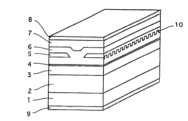
Figs. lA and lB are views showing a first embodiment of the
~ .
CA 022490~3 1998-09-29
invention, which are a general perspective view and a partial
perspective view showing a shape of a diffraction grating,
respectively. This semiconductor laser device is constituted
as one of DFB laser type, in which are sequentially formed a
buffer layer 2 of n-GaAs (thickness t= 0.5 ~m), a cladding layer
3 of n-AlGaAs (Al composition ratio x= 0.4, t= 1.5 ~m), a double
quantum well active layer 4 composed of a non-doped GaAs well
layer (t= 0.008 ~m) / a non-doped AlGaAs barrier layer (x= 0.2,
t= 0.005 ~m), a cladding layer 6 of p-AlGaAs (x= 0.4, t= 1.6
~m), and a contact layer 7 of p-GaAs (t= 1.0 ~m) on a substrate
1 of n-GaAs by using the MOCVD (Metal Organic Chemical
Deposition) method or the like, and a current blocking layer
5 of n-AlGaAs (x= 0.5, t= 0.1 ~m) having a stripe-like window
is embedded in the cladding layer 6. On the bottom face of the
substrate 1 and the top face of thè contact layer 7, electrodes
8 and 9 are respectively formed.
In the AlGaAs materials, as the Al composition is higher,
the band gap tends to become wider. In the embodiment, the band
gap of the cladding layers is wider than that of the active layer
4.
As shown in Fig. lB, a diffraction grating 10 composed of
cyclicbumps anddipsisformedattheactivelayersideinterface
of the current blocking layer 5, and there is no diffraction
grating at a stripe-like window 11 where the current blocking
layer 5 is not present, i.e. a current injection region. On the
CA 022490~3 1998-09-29
diffraction grating 10, the current blocking layer 5 is formed,
and then the cladding layer 6 is formed so as to be embeded in
the window 11.
Next, the operation of the semiconductor laser device will
be described. Upon applying a positive bias voltage to the
electrode 8 of the contact layer 7 and a negative bias voltage
to the electrode 9 of the substrate, an electric current flows
from the contact layer 7 to the substrate 1, and passes through
only a region where the current blocking layer 5 is not formed,
i.e., through the stripe-like window 11, whereby the electric
current density is increased.
The electric current is injected into the active layer 4
as a carrier, and then the carrier re-combines to emit light.
Further, as the injection amount of current increases, induced
emission starts and finally laser oscillation occurs. Part of
the laser light is distributed through the cladding layers 3,
6 disposed on both faces of the active layer 4, further into
the bottom of the current blocking layer 5, and is then guided.
By setting a cycle ~ of the diffraction grating 10 so as
to satisfy the equation (1), only the wavelength ~0 oscillates
selectively, so that a single-mode oscillation is achieved. In
this device, deterioration in crystal property is not caused
in the current injection region or the window 11, so that a DFB
semiconductor laser of low oscillation threshold, high
efficiency and long life time is realized.
14
CA 022490~3 1998-09-29
(Embodiment 2)
Fig. 2 is a perspective view showing a second embodiment
of the invention. This semiconductor laser device is
constituted as one of DFB laser type, in which are sequentially
formed a buffer layer 22 of n-GaAs (thickness t= 0.5 ~m), a
cladding layer 23 of n-AlGaAs (Al composition ratio x= 0.45,
t= 1.5 ~m), a double quantum well active layer 24 composed of
a non-doped AlGaAs well layer (x= 0.1, t= 0.006 ~m) / an AlGaAs
barrier layer (x= 0.3, t= 0.005 ~m), a first cladding layer 25
of p-AlGaAs (x= 0.3, t= 0.15 ~m), a second cladding layer 27
of p-AlGaAs (x= 0.55, t= 1.0 ~m) and a contact layer 28 of p-GaAs
on a substrate 21 of n-GaAs by using the MOCVD method or the
like, and a current blocking layer 26 of n-AlGaAs (x= 0.58, t=
0.1 ~m) having a stripe-likewindow is embeddedbetween the first
claddinglayer25andthesecondcladdinglayer27. Onthebottom
face of the substrate 21 and the top face of the contact layer
28, electrodes 30 and 29 are respectively formed.
In the above constitution, the first cladding layer 25
functions as the optical guide layer for guiding the light
generated in the active layer 24. Moreover, the band gaps of
AlGaAs materials tend to become wider as the Al composition is
higher. In this embodiment, the band gap of the first cladding
layer 25 is wider than that of the active layer 24, and the band
gaps of the lower cladding layer 23 and the upper second cladding
layer 27 are wider than that of the first cladding layer 25.
CA 022490~3 1998-09-29
A diffraction grating 31 composed of cyclic bumps and dips
is formed at an active layer side interface of the current
blocking layer 26, but the diffraction grating is not formed
in the stripe-like window 11 where the current blocking layer
26 is not present, i.e. in the current injection region.
Next, the operation of the above semiconductor laser device
will be described. Upon applying a positive bias voltage to the
electrode 29 of the contact layer 28 and a negative bias voltage
to the electrode 30 of the substrate 21, an electric current
flows from the contact layer 28 to the substrate 21, and passes
through only a region where the current blocking layer 26 is
not present, i.e., through the stripe-like window 11, whereby
the electric current density is increased.
The electric current is injected into the active layer 24
as a carrier, and the carrier then re-combines to emit light.
Further, as the amount of injection current increases, induced
emission starts and finally laser oscillation occurs. Part of
the laser light is distributed through the cladding layer 23
and first cladding layer 25 on both faces of the active layer
24, and further into the bottom of the current blocking layer
26, and is then guided.
By setting the cycle ~ of the diffraction grating 10 so as
to satisfy the equation (1), only the wavelength ~0 oscillates
selectively, so that a single-mode oscillation is achieved. In
this device, deterioration in crystal property is not caused
CA 022490~3 1998-09-29
in the current injection region or the window 11, so that a DFB
semiconductor laser of low oscillation threshold, high
efficiency and long life time is realized.
(Embodiment 3)
Fig. 3 is a perspective view showing a third embodiment of
the invention. This semiconductor laser device is constituted
as one of DFB laser type, in which are sequentially formed a
buffer layer 42 of n-GaAs (thickness t= 0.5 ~m), a cladding layer
43 of n-AlGaAs (Al composition ratio x= 0.24, t= 1.1 ~m), an
optical guide layer 44 of n-AlGaAs (x= 0.2, t= 0.88 ~m), a carrier
blocking layer 45 of n-AlGaAs (x= 0.5, t= 0.02 ~m), a double
quantum well active layer 46 composed of a non-doped InGaAs well
layer (In composition ratio y= 0.2, t= 0.008 ~m) / a non-doped
AlGaAs barrier layer (Al composition ratio x= 0.2, t= 0.006 ~m),
a carrier blocking layer 47 of p-AlGaAs (x= 0.5, t= 0.02 ~m),
an optical guide layer 48 of p-AlGaAs (x= 0.2, t= 0.88 ~m), a
cladding layer 50 of p-AlGaAs (x= 0.24, t= 1.1 ~m) and a contact
layer 51 of p-GaAs on a substrate 41 of n-GaAs by using the MOCVD
method or the like, and a current blocking layer 49 of n-AlGaAs
(x= 0.33, t= 0.1 ~m) having a stripe-like window is embedded
in the optical guide layer 48. On the bottom face of the
substrate 41 and the top face of the contact layer 51 are formed
electrodes 53 and 52, respectively.
The band gaps of AlGaAs materials are wider than those of
InGaAs materials and tend to become wider as the Al composition
.
CA 022490~3 1998-09-29
ishigher. Inthisembodiment,thebandgapsofthe opticalguide
layers 44, 48 are wider than that of the active layer 46, the
band gaps of the cladding layers 43, 50 are wider than those
of the optical guide layers 44, 48, and the band gaps of the
carrier blocking layers 45, 47 are widerthan those ofthe optical
guide layers 44, 48.
A diffraction grating 31 composed of cyclic bumps and dips
is formed at an active layer side interface of the current
blocking layer 49, but the diffraction grating is not formed
in the stripe-like window 11 where the current blocking layer
49 is not present, i.e. in the current injection region.
Next, the operation of the above semiconductor laser device
will be described. Upon applying a positive bias voltage to the
electrode 52 of the contact layer 51 and a negative bias voltage
to the electrode 53 of the substrate 41, an electric current
starts flowing from the contact layer 51 to the substrate 41,
and passes only through the region where the current blocking
layer 49 is not present, i.e., through the stripe-like window
11, whereby the electric current density is increased.
The electric current is injected into the active layer 46
as a carrier, and the carrier then re-combines to emit light.
Further, as the injection amount of current increases,
stimulatedemissionstartsandfinallylaseroscillationoccurs.
Part of the laser is distributed through the optical guide layers
44, 48 disposed on both faces of the active layer 46, and further
18
CA 022490~3 1998-09-29
into the bottom of the current blocking layer 49, and is then
guided. Since the carrier within the active layer 46 is confined
in the active layer because of the carrier blocking layers 45,
47, re-combination efficiency of the carrier is improved.
By setting the cycle A of the diffraction grating 10 so as
to satisfy the equation (1), only the wavelength ~0 oscillates
selectively, so that a single-mode oscillation is achieved. In
this device, deterioration in crystal property is not caused
in the current injection region or the window 11, so that a DFB
semiconductor laser of low oscillation threshold, high
efficiency and long life time is realized.
Though in this embodiment is described the case where the
diffraction grating 61 is formed at the active layer side
interface of the current blocking layer 49 in this embodiment,
the diffraction grating may be formed at the contact layer side
interface of the current blocking layer 49 in the same manner.
(Embodiment 4)
Figs. 4A and 4B are views showing a fourth embodiment of
the invention, which are a general perspective view and apartial
perspective view showing a shape of a diffraction grating,
respectively. This semiconductor laser device is constituted
as one of DFB laser type, in which are sequentially formed a
buffer layer 72 of n-GaAs (thickness t= 0.5 ~m), a cladding layer
73 of n-AlGaAs (Al composition ratio x= 0.24, t= 1.1 ~m), an
optical guide layer 74 of n-AlGaAs (x= 0.2, t= 0.83 ~m), acarrier
19
CA 022490~3 1998-09-29
blocking layer 75 of n-AlGaAs (x= 0.5, t= 0.02 ~m), a double
quantum well active layer 76 composed of a non-doped InGaAs well
layer (In composition ratio y= 0.2, t= 0.008 ~m) / a non-doped
AlGaAs barrier layer (Al composition ratio x= 0.2, t= 0.006 ~m),
a carrier blocking layer 77 of p-AlGaAs (x= 0.5, t= 0.02 ~m),
an optical guide layer 78 of p-AlGaAs (x= 0.2, t= 0.83 ~m), a
cladding layer 80 of p-AlGaAs (x= 0.24, t= 1.1 ~m) and a contact
layer 81 of p-GaAs on a substrate 71 of n-GaAs by using the MOCVD
method or the like, and a current blocking layer 79 of n-AlGaAs
(x= 0.24, t= 0.1 ~m) having a stripe-like window is embedded
in the optical guide layer 78. On the bottom face of the
substrate 71 and the top face of the contact layer 81 are formed
electrodes 83 and 82, respectively.
The band gaps of AlGaAs materials are wider than those of
InGaAs materials and tend to become wider as the Al composition
ishigher. Inthisembodiment,thebandgapsoftheopticalguide
layers 74, 78 are wider than that of the active layer 76, the
band gaps of the cladding layers 73, 80 are wider than those
of the optical guide layers 74, 78, and the band gaps of the
carrierblocking layers 75,77 arewiderthanthoseoftheoptical
guide layers 74, 78.
Furthermore, in place of the diffraction grating 61 for
controlling the wavelength shown in Fig. 3, a grating layer 91
having the same function is provided in this embodiment.
The grating layer 91 is formed by patterning p-GaAs
CA 022490~3 1998-09-29
(thickness t= 0.05~m) in a cyclic manner in the optical guide
layer 78. The grating layer 91 is disposed between the active
layer side interface of the current blocking layer 79 and the
active layer 76, and is formed to have a uniform thickness in
a region of the window 11 and to be cyclic bumps and dips in
regions of both sides of the window 11, thereby acting as a
diffraction grating of the cycle A. By setting the cycle ~ of
the diffraction grating 10 so as to satisfy the equation (1),
only the wavelength ~0 oscillates selectively, so that a
single-mode oscillation is achieved. In this device,
deterioration in crystal property is not caused in the current
injection region or the window 11, so that a DFB semiconductor
laser of low oscillation threshold, high efficiency and long
life time is realized.
(Embodiment 5)
Figs. 5A and 5B are views showing a fifth embodiment of the
invention, which are a general perspective view and a partial
perspective view showing a shape of a diffraction grating,
respectively. This semiconductor laser device is constituted
as one of DFB laser type, in which are sequentially formed a
buffer layer 72 of n-GaAs (thickness t= 0.5 ~m), a cladding layer
73 of n-AlGaAs (Al composition ratio x= 0.24, t= 1.1 ~m), an
optical guide layer 74 of n-AlGaAs (x= 0.2, t= 0.83 ~m), a carrier
blocking layer 75 of n-AlGaAs (x= 0.5, t= 0.02 ~m), a double
quantum well active layer 76 composed of a non-doped InGaAs well
.
CA 022490~3 1998-09-29
layer (In composition ratio y= 0.2, t= 0.008 ~m) / a non-doped
AlGaAs barrier layer (Al composition ratio x= 0.2, t= 0.006 ~m),
a carrier blocking layer 77 of p-AlGaAs (x= 0.5, t= 0.02 ~m),
an optical guide layer 78 of p-AlGaAs (x= 0.2, t= 0.83 ~m), a
cladding layer 80 of p-AlGaAs (x= 0.24, t= 1.1 ~m) and a contact
layer 81 of p-GaAs on a substrate 71 of n-GaAs by using the MOCVD
method or the like, and a current blocking layer 79 of n-AlGaAs
(x= 0.24, t= 0.1 ~m) having a stripe-like window is embedded
in the optical guide layer 78. On the bottom face of the
substrate 71 and the top face of the contact layer 81 are formed
electrodes 83 and 82, respectively.
The band gaps of AlGaAs materials are wider than those of
InGaAs materials and tend to become wider as the Al composition
is higher. Inthisembodiment,thebandgapsoftheopticalguide
layers 74, 78 are wider than that of the active layer 76, the
band gaps of the cladding layers 73, 80 are wider than those
of the optical guide layers 74, 78, and the band gaps of the
carrierblocking layers 75, 77 arewiderthan those of the optical
guide layers 74, 78.
Furthermore, in this embodiment a grating layer 91 having
the same function is provided in place of the diffraction grating
61 for controlling the wavelength as shown in Fig. 3.
The grating layer 91 is formed by patterning p-GaAs
(thickness t= 0.05~m) in a cyclic manner in the optical guide
layer 78. The grating layer 91 is located between the active
CA 022490~3 1998-09-29
layer side interface of the current blocking layer 79 and the
active layer 76, and formed to be cyclic bumps and dips in regions
of both sides of the window 11, thereby acting as a diffraction
grating of the cycle A. The grating layer 91 is not formed in
the region of the window 11. As a method of forming the grating
layer in the regions of both sides of the window 11, a method
of using the selective growth of the grating layer or a method
includingthe steps ofgrowingthe gratinglayer in awhole region
including the window and removing the window part of the grating
layer by ething may be exemplified.
By setting this cycle A so as to satisfy the equation (1),
only the wavelength ~0 oscillates selectively, so that a
single-mode oscillation is achieved. In this device, the
grating layer 91 is absent in the region of the window 11 which
is a current injection region, and the stripe-like window 11
lacks a layer having a different refractive index, which brings
an advantage that the optical mode of the oscillating laser light
is not disturbed.
Though the guide layers are formed of AlGaAs in the above
embodiments, these guide layers are preferably formed of
materials containing few aluminum or no aluminum such as InGaP,
InGaAsP, or AlGaAs (Al composition x: O ~ x ~ 0.3) in these
structures. The guide layer having such a composition improves
the effect of suppressing damages due to oxidation during
formation of the diffraction grating, which allows higher
CA 022490~3 1998-09-29
reliability.
The invention may be embodied in other specific forms
without departing from the spirit or essential characteristics
thereof. The present embodiments arethereforeto beconsidered
in all respect as illustrative and not restrictive, the scope
of the invention being indicated by the appended claims rather
than by the foregoing description and all changes which come
within the meaning and the range of equivalency of the claims
are therefore intended to be embraced therein.
24