Note: Descriptions are shown in the official language in which they were submitted.
CA 022490~7 1998-09-29
INFRARED SENSOR
BACKGROUND OF THE INVENTION
This invention rel.ates to an infrared sensor for
detecting infrared in response to thermal variation due to
absorption of infrared.
DESCRIPTION OF RELATED ART
Infrared detecting el.ements for use in the
infrared sensors have been genera]ly c]assified into
quantum type and thermal type in accordance with
operational principl.e. While the quantum type infrared
detecting element is extremely high in the sensitivity,
there have been such probl.ems due to the necessity of
using lt at lower temperatures with the e]ement itse]f
coo1ed that the sensor is difficu].t to hand]e,
manufacturing costs become high, dimensions in a system
including means for cooling the element become ].arger, and
so on.
In contrast, the therma] type infrared detecting
element is less sensitive than the quantum type but is not
required to be cooled and simpler in the structure, and
has been utilized widel.y in various practical. ways of use,
because of such advantages as l.ow manufacturing costs,
minimized dimensions and so on.
The infrared sensors of this type have been
disclosed in Japanese Util.ity Model Laid-Open Publication
No. 61-50232 by K. Kitamura et al., and U.S. Patent No.
4,258,260 by H. Obara et al..
In a typical arrangement of another known
CA 022490~7 1998-09-29
thermal type sensor, a first infrared detecting e]ement
for infrared detection and a second infrared detecting
element for temperature compensation are concurrent]y
disposed in a container comprising a cap and a stem, and
an infrared shielding plate for preventing the incidence
of infrared onto the second infrared detecting el.ement
from occurring is provided at part of front face of an
infrared transmitting fil.ter closing an incident window
provided in the cap, or the infrared transmitting filter
is provided onl.y at a position opposing the first infrared
detecting element so that the infrared Wll 1 not be
incident on the second infrared detecting element.
In the above sensor arrangement, however, there
is present a space between the second infrared detecting
element for the temperature compensation and the infrared
shielding plate or the like so that, in order to
compl.etely shield the infrared apt to be incident on the
second infrared detecting element, it will. be necessary
that an angle of view of the first infrared detecting
el.ement is set, an aperture is provided for allowing the
infrared only within the range of the set angle of view to
be incident, and an infrared shielding section is provided
to be sufficiently l.arger than the second infrared
detecting element for completely shielding the infrared
present outside the range of set ang]e of view. In this
case, the incidence of infrared to the first infrared
detecting element from a certain direction is caused to be
hindered, so that there wil]. arise a problem that the
CA 022490~7 1998-09-29
sensitivity may happen to be remarkabl.y varied depending
on the direction of incidence of the infrared.
SUMMARY OF THE INVENTION
An object of the present invention is to
overcome the foregoing problems and to provide an infrared
sensor capable of restraining any deterioration in the
detecting precision due to variation in the ambient
temperature, only at lower costs required.
According to the present invention, the above
object can be attained by means of an infrared sensor
wherein first and second infrared detecting elements have
respectivel.y a temperature sensing section provided for
converting a temperature variation of the section due to
incident infrared into an electric detection signal, and
the temperature sensing section is disposed in a container
having an infrared incident window for enl.arging the
temperature variation, characterized in that the first
infrared detecting element for infrared detection and the
second infrared detecting element for temperature
compensation are disposed in the conta1ner, the
temperature sensing section of the first infrared
detecting element is supported in non-contacting state
with respect to a supporting part of a supporting
substrate for the element, the first infrared detecting
el.ement is supported by the supporting substrate in
opposition to the infrared incident window, and the second
infrared detecting element is shie]ded by the supporting
substrate of the first infrared detecting element from the
CA 022490~7 1998-09-29
infrared incident. With this arrangement of the infrared
sensor, it is enabled to restrain any deterioration in the
detecting precision of the infrared due to variation in
the ambient temperature without causing any hindrance to
the compensation for the ambient temperature nor any
increase in the costs, while the second infrared detecting
element for the temperature compensation is disposed in
the same container as that of the first infrared detecting
element.
Other objects and advantages of the present
invention shall become cl.ear as the description of the
invention advances as detailed with reference to preferred
embodiments shown in accompanying drawings.
BRIEF DESCRIPTION OF THE DRAWINGS
FIGURE la shows in a pl.an view an infrared
detecting element employed in the infrared sensor
according to the present invention;
FIG. lb is a sectioned view of the el.ement of
FIG. la taken along l.ine X-X;
FIGS. lc to le, FIGS. lf to lh, FIGS. li to lk
and FIGS. ll. to lo are respective]y explanatory views for
manufacturing steps in different aspects of the infrared
detecting element employed in the present invention;
FIGS. 2 and 3 show in simil.ar plan and sectioned
views in another aspect of the infrared detecting element
employed in the sensor according to the present invention;
FIG. 4 shows one of circuit arrangements
empl.oyable for the infrared sensor according to the
CA 022490~7 1998-09-29
present invention;
FIG. 5 shows another exampl.e of the circuit
arrangement employable in the present invention;
FIG. 6 shows in a schematic sectioned view an
embodiment of the infrared sensor according to the present
invention; and
FIGS. 7-17 are schematic sectioned views showing
other embodiments of the infrared sensor according to the
present invention.
While the present invention shall. now be
described with reference to the preferred embodiments
shown in the drawings, it should be appreciated that the
intention is not to ]imit the invention only to these
aspects and embodiments shown but rather to incl.ude all
alterations, modifications and equival.ent arrangements
possible within the scope of appended c]aims.
DETAILED DESCRIPTION OF THE PREFERRED EMBODIMENTS
In an infrared detecting el.ement 1 employed in
the present invention as shown in FIGS. la and lb, a fil.m
section 4 consisting of a dielectric fil.m is constituted
by forming the dielectric film on a supporting part 3
consisting, for example, of a Si substrate, and providing
in the supporting part 3 a cavity or recess, and a
temperature sensing section 5 for absorbing the infrared
on the film section 4. Further, a microbridge structure
is constituted by providing diaphragm parts or slits in
the film section 4. Whil.e it is desirable fundamental.l.y
that a second infrared detecting element for temperature
CA 022490~7 1998-09-29
compensation is prepared in the same structure as that
described above of the first infrared detecting el.ement 1
for the infrared detection so that both e]ements may be
empl.oyed in an infrared sensor according to the present
invention later described, they need not be a]ways the
same. Further, the supporting part 3 needs not be limited
to the Si substrate, and may be an alumina substrate or
the 1ike.
The dielectric film is constituted by a fi]m of,
for example, SiO, SiN, SiON or the l.ike, whereas the
temperature sensing section 5 is of a structure in which
such element for grasping temperature variation due to the
incidence of infrared as thermistor, thermocouple,
thermopile, pyroelectric element or SAW e]ement is
provided with electrodes for outputting detection signa]s,
and, as required, the dielectric fi]m of SiO, SiN, SiON or
the ].ike is formed thereon. In attaining thereafter a
bridging structure, in particular, the microbridge
structure at a part of the film section 4 for supporting
the temperature sensing section 5 as shown in FIG. 2, the
part of the film is subjected to such etching as RIE
(reactive ion etching) process for allowing parts of
supporting beams 6 of such diel.ectric fi]m as SiO, SiN,
SiON or the like will be left, to form slits. In forming
the supporting section in a diaphragm shape, the etching
is carried out by means of a SiN-masking or the l.ike
formed on the rear surface. In an event where the etching
is to be carried out from surface side of the film section
.. . .... . . ..
CA 022490~7 1998-09-29
4 to attain a formation of FIG. 3, further, a bored part
is formed on lower side of the temperature sensing section
5 by etching the Si substrate 3 through the si].ts formed
in the film section 4. As an etchant, various ones
including KOH (potassium hydroxide), EDP (ethylenediamine
pyrocatechol), hydrazine, TMAH (tetramethylammonium
hydroxide) may be empl.oyed, whil.e an optimum one of them
should be selected in accordance with such demanded
conditions as protection of the temperature sensing
section 5, the side from which the etching is made with
respect to the film section 4, presence or absence of
contact between the etchant and the surface of the
temperature sensing section 5, and so on.
For an arrangement of non-contact support with
respect to the supporting part 3, further, such aspects as
foll.ows may be employed. As shown in FIGS. lc to le, for
exampl.e, the supporting part 3 is mechanically scraped off
as indicated by arrows, by means of a sandblasting or the
like performed from a surface of the supporting part 3
opposite to the surface on which the temperature sensing
section 5 is formed, while l.eaving the dielectric film
section 4. In scraping off only a predetermined portion
of the part 3, a pattern of resist or the l.ike may be used
as a blasting mask, for easil.y carrying out such limited
area scraping.
As shown in FIGS. lf to lh, further, a
sacrificial l.ayer eventually removed is first made through
a pattern formation on the supporting part 3 at part where
CA 022490~7 1998-09-29
the temperature sensing section 5 is to be formed, the
dielectric fil.m section 4 and sensing section 5 are then
formed on the part 3 and sacrificial layer, and final.l.y
the sacrificial. layer is removed. At this time, the
sacrificial l.ayer may be removed by a etchant used through
etching holes. For the material of the sacrificial layer,
one which can be removed by an etchant not corrosive to
the materials forming the temperature sensing section 5
and film section 4 may be used. Exampl.es of such materia]
will. be polysilicone, aluminum and the l.ike. Further, as
shown in FIGS. li to lk, the arrangement may al.so be
realized by forming the temperature sensing section 5 and
dielectric film section 4 on another substrate 3', joining
the substrate 3' and the sections 4 and 5 onto the
supporting part 3 with the sensing section 5 positioned
within a recess preliminarily made in joining surface of
the supporting part 3, and final.]y removing the another
substrate 3'. It is also possible to realize the
arrangement as shown in FIGS. 1] to lo, wherein the recess
prel.iminarily made in the supporting part 3 is first
filled with an eventually-removed sacrificia] materia],
the diel.ectric film section 4 and temperature sensing
section 5 are formed on this supporting part 3 with the
section 5 disposed above the sacrificial material, and
finally the sacrificial material is removed.
In the first and second infrared detecting
elements 1 and 2 of the same structure (see also FIG. 4),
the temperature sensing section 5 employs an a-SiC
... . . ..
CA 022490~7 1998-09-29
(amorphous-sil.icon carbide) thermistor formed in a
so-called sandwich structure as hel.d between a pair of
electrodes consisting of Cr and of a thickness of about
1500 A. This temperature sensing section 5 is formed in a
square shape of, for example, 500 ~m at one side, and each
support beam 6 of the microbridge structure is made to
have a width of 50 ~m.
Now, the measurement of temperature variation is
enabled by, as shown in FIG. 4, connecting the respective
temperature sensing sections 5 of the first and second
infrared detecting elements 1 and 2 in series, applying to
them a predetermined voltage V, and measuring variation in
the potential Vout at junction point between them. As
shown in FIG. 5, further, it may be a]so possible to
connect a series circuit of externally fixed resistors R1
and R2 in parallel to the series circuit of the elements 1
and 2.
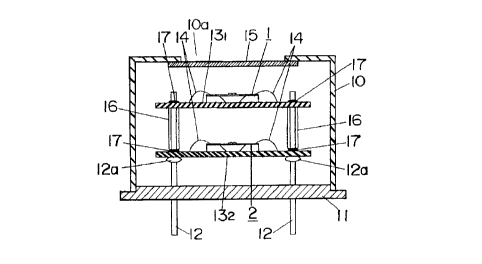
In FIG. 6, there is shown an embodiment of the
infrared sensor according to the present invention, in
which sensor the first infrared detecting element 1 for
the infrared detection and the second infrared detecting
element 2 for the temperature compensation are
respectively of such structure as shown, for example, in
FIG. 3. These first and second infrared detecting
elements 1 and 2 are respectively die-bonded to each of
printed wiring boards 131 and 132 on which wire-bonding
wires are formed, the boards forming the supporting part
3, and the elements 1 and 2 are connected through wires 14
-- 10 --
.
CA 022490~7 1998-09-29
to the respective wires on the printed wiring boards 13
and 132.
On the other hand, a container comprises a
general.l.y cyl,indrical cap 10 and a stem 11 secured as
wel,ded or the l.ike to an axial. end opening of the cap 10
to close the same, whereas the other axial end of the cap
10 is provided with an incident window 10a which is closed
by an infrared transmitting filter 15. Pins 12 acting as
electrodes are fixed to the stem 11 as passed
therethrough, and these pins 12 are inserted into through
holes (not shown) formed in the printed wiring boards 131
and 132 and are fixed thereto as adhered to the boards
through conductive paste 17 for electric conduction. The
printed wiring board 132 on which the second infrared
detecting element 2 is mounted is disposed on l.ower side
(the side of the stem 11) within the container, and
ceramic-made spacers 16 are fitted over the pins 12 for
keeping a predetermined space between the two printed
wiring boards 131 and 132. Further, the printed wiring
board 131 on which the first infrared detecting element 1
is mounted is disposed on upper side (the side of the
incident window 10a) within the container. The pins 12
have flanges 12a of a larger diameter than the through
hole in the printed wiring board 132 50 that the board can
be positioned at a predetermined height from the stem 11.
Further, the respective printed wiring boards
131 and 132 are fixed to the pins 12 with their mounting
surfaces of the infrared detecting el.ements 1 and 2
CA 022490~7 1998-09-29
disposed on the upper side. By disposing thus the element
mounting surfaces of the respective printed wiring boards
131 and 132 on the same side, it is made possible to
prevent the first and second infrared detecting elements
from being damaged upon fixing the pins 12 to the printed
wiring board 131 and 132.
Accordingly, in the present embodiment, the
disposition of the printed wiring board 131 carrying the
first infrared detecting element 1 for the infrared
detection on the upper side of the second infrared
detecting element 2 causes the infrared incident from the
exterior into the incident window lOa through the infrared
transmitting filter 15 (which shal.l be referred to as
"incident infrared" in the foll.owings) to be incident upon
the first infrared detecting el.ement 1 onl.y but to be
prevented from reaching the second infrared detecting
element 2 as shielded by the printed wiring board 131, and
the second infrared detecting element 2 for the
temperature compensation can be prevented from being
influenced by the incident infrared. It is also enabled
to utilize the printed wiring board 131 carrying the first
infrared detecting element 1 concurrently as means for
shielding the infrared with respect to the second infrared
detecting element 2, whereby it is made unnecessary to
separatel.y provide such means as the known infrared
shielding plate, and any restriction of the angle of view
of the first infrared detecting element 1 as well as any
remarkable change in the sensitivity according to the
CA 022490~7 1998-09-29
angle of view can be el.iminated from occurring. As a
result, it should be appreciated that, in cooperation with
the disposition of the second infrared detecting element 2
for the temperature compensation in the same container as
the first infrared detecting element, any deterioration in
the detecting precision due to the variation in the
ambient temperature can be prevented at ]ow costs, without
any hindrance to the compensation for the ambient
temperature.
10Instead of the mounting of the second infrared
detecting element 2 for the temperature compensation to
the printed wiring board 132, the particular el.ement may
be die-bonded directl.y to the stem 11 forming the
container, as shown in FIG. 7, in which event the printed
15wiring board 132 as well as the spacers 16 may be made
unnecessary, and the manufacturing costs can be further
reduced.
Another embodiment of the present invention is
shown in FIG. 8, in which the same basic constituents as
those in FIG. 6 are denoted by the same reference numerals
with their description omitted and on]y characteristic
points shall be described in the followings.
In the present embodiment, the second printed
wiring board 132 carrying the second infrared detecting
element 2 for the temperature compensation is fixed to the
pins 12 with the surface carrying the el.ement faced to the
lower stem side, while the first printed wiring board 131
carrying the first infrared detecting element 1 for the
CA 022490~7 1998-09-29
infrared detection is placed intimately on the second
board with the surface carrying the first element faced to
the incident window lOa both boards are disposed
substantially in the center of the container so that a gap
Ll between the first infrared detecting el.ement 1 and the
infrared transmitting filter 15 and a gap L2 between the
second infrared detecting element 2 and the stem 11 wi].l
be substantially equal to each other (Ll L2) and a l.ayer
of a l.ower refl.ectance material. such as a black paint than
the material of the cap 10 and stem 11 is provided on
inner walls of the cap 10 and stem 11 in order to prevent
the incident infrared from reaching the second infrared
detecting element 2 as refl.ected on the inner wa]ls.
Since other infrared than that incident through
the incident window lOa is also incident on the first
infrared detecting element 1 due to radiation or the like
from the cap 10 and stem 11 of the container the
disposition of the second infrared detecting element to
face the innermost wal] of the container for rendering the
other infrared due to the radiation or the like form the
container to be incident also on the element 2 with the
same intensity al.lows the intensity of the other infrared
incident on both infrared detecting el.ements 1 and 2 than
the incident infrared from the incident window lOa to be
substantial.ly equal whereby any infl.uence due to the
infrared received from the inner wal]s of the container
can be compensated for and the detecting precision can be
prevented from being deteriorated by the ambient
- 14 -
.. . ... .... . . .. .
CA 022490~7 1998-09-29
temperature change.
In the present embodiment, further, the
temperature sensing section 5 in each of the first and
second infrared detecting elements 1 and 2 is constituted
by a thermistor which causes a temperature variation to
occur with its own heat generation, but a driving of the
temperature sensing section 5 with a constant voltage or
current is so performed that the own heat release val.ue
wil1 vary in response to variation in the resistance val.ue
of the thermistor due to the variation in the ambient
temperature. To this own heat release value, the heat
conductance relying on heat insul.ating structure of the
infrared detecting elements 1 and 2 is determinative, and
this heat conductance is determined by a sum of the heat
conductance of the supporting diaphragm or microbridge for
the temperature sensing section 5 and the heat conductance
of ambient gas. Here, the heat conductance of the ambient
gas is l.argel.y influenced by the gap L1 between the first
infrared detecting el.ement 1 and the fi]ter 15 and the gap
L2 between the second infrared detecting el.ement 2 and the
stem 11, and any difference between these gaps causes a
difference to arise in the heat conductance, whereby a
difference is caused to arise in the own heat release
value to render a heat difference to occur in the
temperature sensing section 5.
At this time, in the present instance, the heat
conductance can be made substantiall.y equal with respect
to both temperature sensing sections 5 of the first and
CA 022490~7 1998-09-29
second infrared detecting elements 1 and 2 by
substantially equalizing both gaps Ll and L2, and the
detecting precision can be prevented from being
deteriorated due to the change in ambient temperature by
rendering any temperature rise due to the own heat
generation at the temperature sensing sections 5 to be in
conformity to each other. Further, because of these
respects, it is enabled to realize an infrared sensor
further higher in the detecting precision than the
embodiment of FIG. 6.
Further, because of the provision of the l.ayer
of lower reflectance than the cap 10 and stem 11 by the
application of black paint on the inner wall.s of the
container, it is enabled to prevent the infrared
reflecting on the inner walls of the container even in the
case of wide angle of view, to prevent unnecessary
infrared from being incident on the second infrared
detecting element 2 for the temperature compensation, and,
consequently, to realize an infrared sensor of a wide
angle of view.
In another embodiment shown in FIG. 9 of the
present invention, the first and second infrared detecting
elements 1 and 2 are respectively mounted onto each of
both surfaces of a single printed wiring board 18 having
the printed wirings on the both surfaces, whil.e the second
infrared detecting el.ement 2 is die-bonded to a recess 18a
formed in the surface facing the stem 11 and the board 18
is brought into contact at least at peripheral edges with
- 16 -
. .
CA 022490~7 1998-09-29
the inner walls of the cap 10.
By mounting in this way the first and second
infrared detecting elements 1 and 2 respective]y onto each
of front and rear surfaces of the single printed wiring
board, it is enabled to reduce the manufacturing costs by
the fact that only one printed wiring board 18 is required
for mounting the two elements 1 and 2, and that required
mounting work is simp]ified. It is also possible to
render the recess 18a made in the printed wiring board 18
to have a depth enough for keeping the second infrared
detecting element 2 in the recess 18a as we]l as the wires
14 not to project out of the rear, mounting surface of the
board 18, whereby, when the mounting is made first for the
second infrared detecting element 2 in the recess 18a on
the rear surface and thereafter for the first infrared
detecting element 1 onto the other front surface of the
board 18, the second infrared detecting element 2 mounted
initial can be prevented from being damaged by any jig or
the like that may hit the element 2 upon mounting later
the first infrared detecting element 1.
Further, since the printed wiring board 18 is
brought into contact at the peripheral edges with the
inner walls of the cap 10 of the container, the board 18
is improved in the ability of follow-up to the ambient
temperature, the first and second infrared detecting
elements 1 and 2 are made thereby to well follow the
ambient temperature, and the detecting precision can be
improved by achieving the temperature compensation with
CA 022490~7 1998-09-29
the ambient temperature precisely monitored.
In the present embodiment, further, a gas
communicating hole 18b is made as passed through the
printed wiring board 18, and Xe gas of a l.ow heat
conduction is seal.ed in the container. In substituting
the low heat conduction gas for air inside the container
for improving the sensitivity or in sealing the interior
of the container by drawing a vacuum, therefore, it is
made easier to discharge the gas in a space partitioned by
the printed wiring board 18 on upper side thereof through
the gas communicating hol.e 18b made in the board 18, and
there arises an advantage that an improvement in the
productlvity as well. as a reduction in the manufacturing
costs can be attained.
In the embodiment of FIG. 9, other constituents
are the same as those in the embodiment of FIG. 6 and are
denoted by the same reference numera].s as those used in
FIG. 6.
In FIG. 10, another embodiment according to the
present invention is shown, in which the stem 11 of the
container is molded integral with the pins 12 passed
through the stem, and the short cylindrical cap 10 made of
a metal, for example, is fitted over one front surface of
the stem to be closed by the latter at one end opening, to
define the space between them. The other end opening is
closed by the infrared transmitting filter 15.
Within the space and on top ends of the pins 12
erected from the stem 11, the printed wiring board 13 is
- 18 -
.......... . .
CA 022490~7 1998-09-29
secured, and the infrared detecting element 1 and a
thermistor 7 as a contact type temperature sensor for
measuring the temperature of the element 1 are mounted on
the board 13. Here, the pins 12 may be provided to act
also as output terminals for signal.s of the element 1 and
thermistor 7. Further, the cap 10 defining the interior
space in conjunction with the stem 11 is provided on the
inner surfaces with thin heat radiating fins lOc.
With the provision of the heat radiating fins
lOc, further, the time constant at which the temperature
of the cap 10 coincides with the temperature of the
interior space defined by the cap 10 and stem 11 can be
made smaller, the temperature of the infrared detecting
element 1, thermistor 7 as a temperature detecting means,
cap 10 and stem 11 can be quickly stabi]ized even in the
circumstances where the ambient temperature is apt to
vary, and the temperature can be measured at a high
precision. Further, with the temperature of the infrared
detecting element thus enabl.ed to be measured by means of
the thermister, it is made possible to correct any error
in output signals occurring due to the ambient temperature
variation, and the detecting precision can be further
elevated.
Since the infrared detecting element 1 and
thermistor 7 in the foregoing embodiments of FIGS. 9 and
10 are mounted on the single printed wiring board 13,
further, they vary at the same temperature gradient, so as
to be able to elevate the detecting precision even in a
-- 19 --
CA 022490~7 1998-09-29
state where the variation in the ambient temperature
occurs.
In another embodiment shown in FIG. 11 of the
present invention, the cap 10 in the embodiment of FIG. 10
is replaced by a cap lOA made with two metal members
joined to be a double structure having an interior gap lOa
filled with air.
While in the present embodiment the interior of
the cap lOA is made to be the air layer lOa, the same is
not required to be limited thereto but the interior may be
fil.led with other gas or may even be drawn a vacuum.
Normally, the cap lOA and stem 11 are different
in the heat capacity due to the difference in the
thickness so that, in an event of variation in the ambient
temperature, the temperature variation is apt to occur
initially on the side of the cap lOA, but the present
embodiment employing the cap lOA of the double structure
having in the interior the air l.ayer lOa is capable of
moderating the temperature fl.uctuation in the inner wall
surface of the cap lOA, so that the infrared fl.ux from the
inner wall. surface of the cap lOA and stem 11 to the
infrared detecting elements 1 and 2 will. be substantial]y
identical, and the detecting precision can be improved.
Further, as the temperature fluctuation in the space
defined by the cap lOA and stem 11 can be moderated, the
temperature fluctuation at the infrared detecting el.ements
1 and 2 and thermistor 7 can be also moderated, so that
any difference in the temperature between these el.ements
- 20 -
. . .
CA 022490~7 1998-09-29
can be minimized to render the detecting precision more
excellent.
In the embodiment of FIG. 11, on the other hand,
it is also possible to emp]oy a vacuum pressure
arrangement with the interior space of the cap 10 and stem
11 drawn a vacuum preferably to be bel.ow 1 Pa. In this
case, the thermal. conduction from the cap 10 and stem 11
to the infrared detecting elements 1 and 2 and thermister
7 is remarkably reduced even upon change in the ambient
temperature, so as to relieve the temperature fluctuation,
accordingly any temperature difference is l.ess caused to
occur between these constituents, and the detecting
precision can be further improved.
Other constituents of this embodiment are the
same as those in the embodiment of FIG. 10, and the same
constituents as those shown in FIG. 10 are denoted in FIG.
11 by the same reference numerals as used in FIG. 10.
In another embodiment shown in FIG. 12 of the
present invention, the container is constituted simil.arly
with the stem 11 molded integrally with the pins 12, and
the short cylindrical cap 10 a bottom end opening of which
is closed by the stem 11 to define an interior space,
while the top end of the cap 10 is formed to have the
incident window closed by the infrared transmitting fil.ter
15.
Within the interior space defined by the cap 10
and stem 11, the infrared detecting element 1 and the
thermistor 7 as the contacting type temperature detecting
CA 022490~7 1998-09-29
element for measuring the temperature of the infrared
detecting element 1 are mounted on the stem 11, and the
pins 12 are also acting as the signa]. output terminals of
the element 1 and thermistor 7.
As a distinguishing feature here, the cap 10 and
stem 11 are formed to have substantia]]y the same
thickness.
In the present embodiment, therefore, the cap 10
and stem 11 can be made to have an identical. or the same
level of the heat capacity by the same thickness, so that
there arises no uneven temperature variation as the same
temperature variation takes pl.ace in the cap 10 and stem
11 even upon variation in the ambient temperature, the
infrared flux from the inner wall. surface of the cap 10
and stem 11 to the respective infrared detecting elements
1 and 2 can be made substantially identical., and the
detecting precision can be improved.
In another embodiment shown in FIG. 13, in
contrast to the embodiment of FIG. 10, such paint lOb of
which the radiant emissivity is prel.iminarily known as the
black paint is applied to parts of the inner wal.l.s of the
cap 10 and stem 11 which are included in the ang]e of view
of the infrared detecting el.ements 1 and 2. In the
present instance, the infrared radiant emissivity is made
constant on the inner surface of the cap 10 and stem 11
included in the angl.e of view of both elements 1 and 2,
the infrared flux from the inner surface to the elements 1
and 2 will. be made substantially identical., and the
CA 022490~7 1998-09-29
detecting precision can be improved.
In the embodiment of FIG. 13, further, the paint
10b may be rep].aced by a use or exec~tion of a mater1a]
for the whole or for surface layer or of a surface
treatment with respect to the cap 10 and stem 11 and
attaining the same effect as the paint 10b.
Other constituents of the present embodiment are
the same as those in the embodiment of FIG. 10, and the
same constituents are denoted in FIG. 13 by the same
reference numerals as those in FIG. 10.
As another embodiment, the bl.ack paint 10b in
FIG. 13 is replaced by a pl.ating of metal or the like to
attain a lower radiant emissivity. In this case, the
lower radiant emissivity at the inner walls of the cap 10
and stem 11 at least at portions included in the angle of
view of the infrared detecting elements 1 and 2 renders
the infrared flux from the inner wal]s of the cap 10 and
stem 11 to the elements 1 and 2 to be smal.l enough to be
substantial.l.y the same even when a temperature difference
arises between the cap 10 and the stem 11 due to any
variation in the ambient temperature, and the detecting
precision can be improved. In this case, it is al.so
preferabl.e to attain a mirror finish at the surface of the
cap 10 and stem 11.
In another embodiment of the present invention
as shown in FIG. 14, a further thermistor 9 is provided as
adhered to an inner wall of the cap 10, in contrast to the
embodiment of FIG. 10. In this case, it is made possibl.e
CA 022490~7 1998-09-29
to predict an extent of variation in the output of the
infrared detecting el.ement 1 due to the temperature
variation of the cap 10, by measuring the temperature of
the cap 10 by means of the thermistor 9.
Other constituents of thls embodiment are the
same as those in the embodiment of FIG. 10, and the same
constituents are denoted in FIG. 14 by the same reference
numerals as those in FIG. 10.
In still another embodiment of the present
invention as shown in FIG. 15, there are provided a
plurality of the thermistors 7 for detecting the
temperature at respective portions of the cap 10, stem 11,
infrared transmitting fi].ter 15, infrared detecting
element 1 and printed wiring board 13.
The calorie which is detected by the infrared
detecting element 1 can be represented by a formula
~a-~a(Ta -Ts4) ................. (1)
wherein ~a is the ratio of the angl.e of view at the
incident window of the cap 10, ~a is the radiant
emissivity of an objective, Ta is the temperature of the
objective, and TS is the temperature of the infrared
detecting element 1.
In an event where the ambient temperature is
stable and the temperature at portions of the package
within the angle of view of the infrared detecting element
1 (at the cap 10, stem 11 and infrared transmitting filter
15) coincides with the temperature of the infrared
detecting element 1, the relation of incident infrared
- 24 -
CA 022490~7 1998-09-29
flux at the infrared detecting element to the e]ement
temperature and to the objective temperature can be
obtained with the above formula (1), whereas, as the
ambient temperature varies to render the temperature at
the package portions in the angle of view of the element 1
to be different from the temperature of the element 1,
then the infrared from the package is caused to be
detected in addition to the infrared from the objective,
and there occurs an error.
Here, the temperature correction factor at the
package portions can be represented by a formula
(T14-Ts4)+~2~2(T24-Ts )+ ~-- +~n- n( n s
..... (2)
wherein ~n denotes the ratio of the angle of view at the
package portions n, ~n denotes the radiant emissivity at
the package portions n, and Tn denotes the temperature at
the package portions n.
Now, by applying the output from the thermistors
7 to the above formula (2) and obtaining the sum or
difference of the formulas (1) and (2), it is made
possible to improve the detecting precision.
In another embodiment of the present invention
as shown in FIG. 16, there is a difference from the
embodiment of FIG. 10 in that, instead of the separate
provision of the thermistor 7 as the temperature detecting
means, the temperature of the temperature sensing section
itself of one or both of the infrared detecting elements 1
and 2 is measured, for the correction of the detected
- 25 -
CA 022490~7 1998-09-29
signals with the thus measured temperature value. More
specifically, the temperature sensing section of these
infrared detecting elements is constituted by the
thermistor, and the temperature of the temperature sensing
section is measured by obtaining the resistance value of
the thermistor. While in the foregoing formu].a (1) the
temperature Ts is denoted as that of the infrared
detecting element, the infrared from the objective is to
be received at the temperature sensing section in
practice, and the temperature TS should be denoted
inherently as that of the temperature sensing section of
the infrared detecting element. When the general.
temperature variation is small., on the other hand, there
arises no remarkabl.e temperature difference between the
temperature sensing section and the separately provided
temperature detecting means, and the temperature T may be
denoted as the temperature of the infrared detecting
element.
Here, in the case where the temperature
difference is apt to occur between the respective parts in
such event that the temperature at the respective parts of
the sensor is varying due to the variation in the ambient
temperature, there occurs the temperature difference
between the temperature sensing section and the
temperature detecting means, and it wil.l. be required, for
accurate detection, to measure the temperature of the
temperature sensing section in the infrared detecting
el.ement. Since in the present embodiment the temperature
- 26 -
CA 022490~7 1998-09-29
of the temperature sensing section itself is measured the
detection is enabled at a higher precision.
In the present invention various design
modification is possible within the scope of appended
claims. In the embodiment of FIG. 14 for example the
thermistor 9 provided on the inner surface of the cap 10
may be omitted as shown in FIG. 17 to employ only the
single thermistor 7 mounted on the supporting substrate 13
along with the first infrared detecting element 1 for
simplifying the arrangement in adaption to the use.
Further it should be appreciated that the embodiments of
FIGS. 10 through 17 are respectively capable of mutual~y
incorporating their characteristic arrangement of another
embodiment.
, .. .. . . . .