Note: Descriptions are shown in the official language in which they were submitted.
CA 02249085 1998-09-29
S
XDSL SPLTTTER ASSEMBLY FOR MAIN DISTRIBUTION FRAME
TECI-INICAL FIELD OF THE INVENTION
The present invention relates to a xDSL sputter block for mounting on a
central
oglce telecommunications main distribution frame with xDSL sputter circuits
housed
therein.
CA 02249085 1998-09-29
BACKGROUND OF THE INVENTION
ADSL (Asymmetric Digital Subscriber Line) is a modem technology that transmits
multimedia and high speed data over existing twisted-pair telephones lines
concurrently
with Plain Old Telephone Service (POTS). VDSL is a higher speed variation of
ADSL.
The term xDSL will be used herein to generically refer to these different
versions of
transmitting additional signals over twisted pair concurrently with the POTS
signal. The
term "additional signals" will be used to refer to any signal other than POTS
that is
transmitted over the existing POTS lines. The term "combined signals" will be
used to
refer to both the additional signals and POTS signals combined over a line. An
xDSL
circuit connects an xDSL modem on each end of a twisted-pair telephone line,
that is, at
the "central office" (or node) and at the premises of the subscriber (or
customer). The
xDSL modem in the central office transmits and receives the additional signals
through a
"splitter" that combines the downstream (to the subscriber) additional signals
onto the
POTS line or filters offthe upstream (from the subscriber) POTS signals.
The terms "splitting" or "splitter" are used to refer to a circuit, for
example, a low
pass filter or low pass and high pass filter combination, that at least
separates a POTS
signal from a combined signal in the case of the example of a low pass filter
and separates
both the POTS and xDSL signals from the combined signal in the example of the
low pass
and high pass filter combination. In other words, the signal upstream from the
splitter to
the xDSL modem may or may not have the POTS signal filtered off since xDSL
modems
may incorporate high pass filters and may not be affected by or even see the
POTS signals
being transmitted with the xDSL signals. One reason for removing the POTS
signal from
the xDSL signal is to deny access to the POTS signal when the modem is
controlled by
CA 02249085 1998-09-29
someone other than the telephone company. Circuits have been developed which
perform
this splitting function and the structure and nature of the various sputter
circuits form no
part of the present invention other than the fact that they are at the
intersection of three
signal paths - the additional signals, POTS signals and the combined signals -
and must be
interconnected into an xDSL/POTS network in some manner.
Sputters are typically housed with the xDSL modems. However, there are
problems with the sputter being located in the modem. For example, inefficient
backtracking of wiring occurs. The POTS line cards and the main distribution
frame
where the cross-connect and protector functions are located are already in
place in the
central office. The network switches and equipment for the xDSL circuit are
added
somewhere in the central offce and the POTS signal would have to be routed
from
somewhere in the existing POTS network to the xDSL modem to be combined with
the
addition signal and then back to the existing twisted-pair network. If the
POTS signal is
taken to the splitter in the modem and the modem needed to be repaired it
could require
interrupting the POTS service which is a life line service to the subscribers.
Also,
telephone companies may be required to provide access to their xDSL network to
competitive carriers as part of regulatory changes. Having the splitter in the
modem may
make it inconvenient to provide such competitive access. Therefore a need
exists for a
means to better accommodate xDSL splitters in the central ofI'lce to help
avoid such
backtracking, take the POTS signal out of the modem, and provide a better
location for
access to competitive carriers.
However, space in the existing central ofI'lces is often hard to find.
Commonly the
floor of central o~ces is already filled with existing main distribution
frames. Therefore a
CA 02249085 1998-09-29
need exists to be able to prevent such backtracking in a space saving manner
taking into
account existing hardware in the central office.
4
CA 02249085 1998-09-29
SUMMARY OF THE PRESENT INVENTION
The present invention eliminates POTS signal backtracking to the modem,
preserves space, is usable with traditional wiring center organization
practices and
prevents POTS interruptions by providing a sputter assembly for mounting on
the main
distribution frame to connect the splitter circuit into the cross-connect
field of the main
distribution frame. In one aspect, the present invention provides a main
distribution frame
comprising a frame and a first array and a second array of terminal blocks
mounted on the
fi-ame. The terminal blocks carry arrays of terminals with each ternunal for
termination of
at least two wires for electrical connection thereof. A portion of the
terminals of the
terminal blocks of the first array are connected to a portion of the terminals
of the terminal
blocks of the second array by a plurality of first jumpers to create a cross-
connect field.
The assembly also comprises at least one splitter circuit located on the frame
for
combining/splitting xDSL signals and POTS signals carried over separate wire
pairs
onto/from a single wire pair. The circuit has a first pair of contacts for
connection to a
wire pair carrying the POTS signal, a second pair of contacts for connection
to a wire pair
carrying the xDSL signal, and a third pair of contacts for connection to a
wire pair
carrying the combined POTS and xDSL signals. At least one of these pairs of
contacts is
connected to a pair of the terminals of one of the terminal blocks.
Another aspect of the present invention provides a terminal block assembly for
mounting to a main distribution frame comprising a terminal block having an
array of
terminals there through with each terminal for termination of two wires
thereto for
electrical connection thereof. The assembly also comprises at least one
sputter circuit for
combining/splitting first and second signals onto/from a single telephone wire
pair, the
s
CA 02249085 1998-09-29
..
circuit having a first pair of contacts for carrying the first signals, a
second pair of contacts
for carrying the second signals, and a third pair of contacts for carrying the
combined first
and second signals. At least one of the pairs of contacts is connected to a
pair of the
terminals of the terminal block.
In a further aspect of the present invention, a splitter assembly is provided
comprising a terminal block having an array of terminals therethrough with
each terminal
having a front end and a rear end. The array of terminals is divided into a
POTS field with
the front ends of the terminals for being connected to POTS lines from a
central once, an
xDSL field with the front ends of the terminals for being connected to xDSL
lines, and a
jumper field with the front ends of the terminals for being connected to
jumpers. The
assembly also comprises at least one xDSL splitter circuit having POTS
contacts
connected to the rear ends of the terminals in the POTS field, xDSL contacts
connected to
the rear ends of terminals in the xDSL field, and jumper contacts connected to
the rear
ends of the terminals in the jumper field.
The present invention eliminates POTS signal backtracking to the modem by
taking the splitter out of the modem and moving it to the main distribution
frame where
'POTS lines from the central oi~lce are cross-connected with the outside plant
lines. The
present invention also preserves space by being locatable on existing main
distribution
frames without violating clearance requirements. It is also usable with
traditional wiring
center organization practices and being usable with known main distribution
frames and
terminal blocks, craftspeople can use existing tools and procedures at a
familiar location.
The present invention prevents POTS interruptions that may be caused by having
POTS
signal taken to a modem that may need to be repaired or replaced.
CA 02249085 1998-09-29
BRIEF DESCRIPTION OF THE DRAWINGS
Figure 1 is a front view of the preferred embodiment of the xDSL sputter
assembly of the
present invention open;
Figure 2 is a side view of the assembly of Figure 1 open;
Figure 3 is a partially exploded perspective view of the assembly of Figure 1
closed;
Figure 4 is a diagram of connections for an xDSL sputter assembly of the
present
invention;
Figure 5 is a perspective view of an alternative embodiment of an xDSL sputter
assembly
of the present invention;
Figure 6 is a perspective view of the assembly of Figure 5 mounted on a
distribution
frame;
Figure 7 is a perspective view of an alternative embodiment of an xDSL sputter
assembly
of the present invention;
Figure 8 is a perspective view of the assembly of Figure 7 mounted on a
distribution
frame;
Figure 9 is a perspective view of an alternative embodiment of an xDSL
splitter assembly
of the present invention with the cover exploded;
Figure 10 is a diagram of an alternative embodiment of connections for a
sputter assembly
of the present invention;
Figure 11 is a diagram of a further alternative embodiment of connections for
a splitter
assembly of the present invention; and
Figure 12 is a diagram of a further alternative embodiment of connections for
a splitter
assembly of the present invention.
CA 02249085 1998-09-29
y
DETAILED DESCRIPTION OF THE INVENTION
One aspect of the present invention provides splitter assembly 10 shown in a
preferred embodiment in Figure 1-4 that is adapted to be mounted on main
distribution
frame 34 (shown in Figure 6 with another embodiment of assembly 10' mounted
thereon)
and readily connected into the cross-connect arrangement of central office
distribution
frames.
With reference to Figure 6, main distribution frames are typically one of a
few
kinds of common formats with a first array of terminal blocks mounted in first
mounting
area 36 and connected between a central oglce cable and jumpers, and a second
array of
terminal blocks mounted in second mounting area 38 and connected between the
jumpers
and the outside plant cables. The terminal blocks in the first array of
terminal blocks are
typically referred to as "terniinal blocks" and examples include the terminal
block
disclosed in U.S. Patents Nos. 4,763,226 and 4,766,521 known as the Versablock
terminal
block, DF 300 terminal blocks sold by Siecor Corporation, NE 66 blocks, and
rotating
terminal blocks. The second array of terminal blocks are referred to as
"central office
connectors", "protector/connector blocks" or "protector blocks" and examples
include
blocks sold by Siecor corporation under numerical designations of 303, 310,
377, 388,
390, 391, and QCM486. The "connectors" often incorporate protectors and test
points in
addition to a block of wire terminals. To avoid confusion of terms, "terminal
block" will
be used herein as a generic term to include both terminal blocks,
"connectors", "protector
blocks" and any other type of block that is used as part of a cross-connect
arrangement
between two cables.
s
CA 02249085 1998-09-29
In a common architecture, the phone lines from the POTS switch are connected
to
the first array of terminal blocks, the phone lines from the outside plant are
connected to
the second array of terminal blocks, and jumpers are then connected between
the first
array and second array of terminal blocks to provide the cross-connect field.
This cross-
connect field provides a place where the outside plant lines can be rearranged
relative to
the central offce lines. Typically there are more terminal blocks in the
second array
connected to outside plant than terminal blocks in the first array because
outside plant
lines are installed to plan for fixture growth while central office lines can
be added more
readily to track current demand. As such, there is commonly more space
available in the
first mounting area than the second mounting area.
There are other formats for main distribution frames, for example, front
facing
frames (the frame partially shown in Figure 8 is an example) where the first
and second
array of terminal blocks are on the same side of a frame mounted against a
wall. There are
also modular distribution frames that are intended to be easier to install
than the traditional
main distribution frames. One thing that all these frames have in common is
the competing
design considerations of 1) high density of terminals to save space and 2)
suglcient space
for craftspeople to connect wires and route jumpers. The first consideration
is often
addressed by increasing the density of terminals on the terminal blocks and
the second
consideration is often addressed by requiring certain clearances around each
terminal
block to allow for movement of installers' hands during connection of wires
and the
routing of jumpers. With some distribution frames, the height and width of the
terminal
blocks must be within a certain envelope so that when the terminal blocks are
mounted at
the various mounting locations, there are set distances between neighboring
terminal
CA 02249085 2006-O1-11
blocks in the horizontal and vertical directions. The terminal block of the
'521 and '226
patents is an example of a terminal block with a height and width within a set
envelope and
the patents deal with increasing the number of terminals in the terminal block
while
maintaining the height and width requirements of the housing.
wth reference to Figures 1-4, the preferred embodiment of xDSL sputter
assembly 10 of the present invention is shown. Sputter assembly 10 has housing
12 which
defines interior 14 with open side 16. Terminal block 18 is pivotally attached
to housing
12 and has front face 20 and rear face 22 with array 24 of terminals 26
mounted in
terminal block 18 such that terminals 26 have first and second ends, for
example, front
ends 28 accessible at front face 20 and rear ends 30 accessible at rear face
22. Terminals
26 are for termination of at least two wires for electrical connection of the
two wires.
Terminals may be any of a variety of terminals, for example, wire wrap pins,
insulation
displacement (mC) pins, pins for soldering, connectors or other kind of
electrical contact.
Terminal block 18 can be closed over open side 16 and pivoted away from open
side 16 to
allow access to rear face 22 of terminal block 18 as well as interior 14 of
housing 12. In
the preferred embodiment, terminal block 18 and the outer structure of housing
12 and the
mounting and latching features of terminal block 18 to housing 12 are
substantially those
of the terminal block disclosed in U.S. Patent Nos. 4,766,521 and 4,763,226 to
Pelletier
and more specifically the current commercial embodiment of the block disclosed
in these
patents sold by Siecor Corporation under the trademark Versablock.
The '521 and '226 also offer a further explanation of terminal block 18 and
its
cooperation with housing 12.
- _ CA 02249085 1998-09-29
2. .
As discussed above there are a variety of distribution frames 34 commercially
available and they all generally serve the function of providing a cross-
connect field
between two groups of cables, for example, the telephone company central once
cables
and the outside plant telephone cables. As disclosed in the '521 and '226
patents, the
terminal block provides a cross-connect field where a cable is terminated on
rear ends 30
of terminals 26 at rear face 22 of the terminal block and cross-connect
jumpers are
connected to front ends 28 of terminals 26 on front fi~ce 20 of the terminal
block. As is
known in the art of distribution frames, some of the terminals of the terminal
blocks in the
first array are connected to some of the terminals of the terminal blocks of
the second
array by a plurality of jumpers to create a cross-connect field whereby
rearrangement of
the telephone network lines can be achieved by simply rearranging the jumpers.
By having
the jumpers attached to the front faces of the blocks, they are more
accessible for any
rearranging. The cables that are being cross-connected are connected on the
rear faces of
their respective set of blocks. As such, the entire array of terminals of the
terminal block
of the '521 and '226 patents is dedicated to the connection of a cable to a
set of jumpers,
with one face of the terminal block for termination of one of the cables to be
cross-
connected and the other face for termination of the jumpers.
One aspect of the present invention provides an xDSL splitter in the terminal
block
and divides the array of terminals into a first, second and third fields to
accommodate
connecting of the splitter into the cross-connect arrangement. Specifically in
the preferred
embodiment, interior 14 of housing 12 has cards 40 with xDSL splitter
circuitry
components 42 mounted thereon. Each card 40 has two opposed sliding edges 44
a, b
that are slidably received in card guides 46 mounted in interior 14. One card
40 may have
m
CA 02249085 1998-09-29
more than one xDSL splitter circuit thereon, and in the embodiment of Figures
1-3, two
circuits are on each card. Card retainer 48 holds cards 40 in place once
installed and is
shown by example as flexible strip 50 with reduced cross-section ends 52 that
are inserted
into holes 54 in housing 12. Strip 50 is readily inserted and removed by
flexing to remove
ends 52 from holes 54 to allow removal of cards 40. As an alternative, strip
50 may be
eliminated and retention of the cards may be provided by use of any type of
snap-in feature
on the card guides or the housing to hold the cards.
With fizrther reference to the diagram of Figure 4, the connection of the xDSL
splitter circuits are shown. Array 24 of terminals 26 is divided into first,
second, and third
fields, for example, POTS field 60, xDSL field 62 and jumper field 64,
respectively.
POTS lines 70 carrying the POTS signal are connected to front ends 28 of
terminals 26 in
POTS field 60, xDSL lines 72 are connected to front ends 28 of terminals 26 in
xDSL
field 62 and jumpers 74 are connected to front ends 28 of terminals 26 in
jumper field 64.
The POTS lines, xDSL lines and jumpers are wire pairs. Splitter circuit 78 has
a first,
second, and third pair of contacts, for example, POTS contacts 80 connected to
rear end
30 of a terminal in POTS field 60, xDSL contacts 82 connected to rear end 30
of a
terminal in xDSL field 62, and jumper contacts 84 connected to rear end 30 of
a terminal
in jumper field 64.
In the embodiment of Figures 1-5, pairs of contacts 80, 82, and 84 are
connected
to rear ends 30 by wires 88 that have first end 90 connected to rear ends 30
of terminals
26 and second ends 92 connected to circuit 78 on card 40. Wires 88 allow
terminal block
18 to be pivoted while maintaining the connections from the circuits to the
terminals.
Terminal block 18 is pivoted up to open interior 14 of housing 12 to allow
insertion of the
12
CA 02249085 1998-09-29
..--...
desired number of cards 40 into card guides 46 and then card retainer 48 is
inserted to
retain cards 40. Preferably, wires 88 are already connected at second ends 92
to cards 40
and first ends 90 of wires 88 are then connected to the respective rear ends
30 of terminals
26. Wires 88 can be connected to cards 40 in any way, for example, soldering,
using a
connector, insulation displacement connectors, wire wrap pins, etc. Then
terminal block
18 is lowered back down and snap closed over interior 14. As assembled,
assembly 10
can then be conveniently mounted to distribution frame 34 and POTS lines are
connected
to the front end of terminals in the POTS field, xDSL lines are connected to
the front end
of terminals in the xDSL field, and jumpers are connected to the front end of
terminals in
the jumper field.
It is preferred that assembly 10 is mounted in the first mounting area at a
terminal
block mounting location among the first array of conventional terminal blocks.
Jumpers
74 can then preferably be routed one of two ways. First, jumpers 74 may be
considered
analogous to a cable to be cross-connected and routed to the rear ends of
terminals in a
conventional terminal block in the first array and then conventional jumpers
are routed
from the front of the conventional terminal block in the first array to the
front faces of
terminal blocks in the second array as is standard. Alternatively, jumpers 74
may be
considered analogous to conventional jumpers and routed directly to the front
faces of
terminal blocks in the second array. The method chosen may depend on the
nature of the
central office network and any considerations dictated by co-location
requirements that
may require telephone companies to provide access points to their networks to
other
telephone companies.
13
CA 02249085 1998-09-29
By using a modified housing and terminal block of the '521 and '226 patents,
assembly 10 has the same height and width of standard terminal blocks such as
the block
of the '521 and '226 patents and does not violate clearance requirements when
mounted
on frame 34. Assembly 10 may have a greater depth than the terminal blocks of
the '521
and '226 patents if needed to better accommodate cards 40.
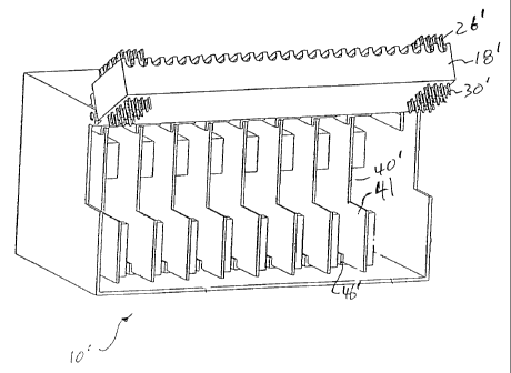
Figure 5 shows an alternative embodiment of assembly 10' where terminal block
18' has a reduced height such that it does not close completely over interior
14'. Due to
the size of sputter circuits 78' it may be that a full size terminal block 18
is not required.
Terminal block 18' in Figure 6 has six (6) rows of terminals 26' so that each
column of
terminals can be connected to the six contacts of sputter circuit 78. By
shortening the
terminal block, additional area is provided underneath terminal block 18' for
cards 40' to
extend to provide additional area for circuits 78 as shown by stepped portion
41 of cards
40. Terminals 26' in this embodiment have a wire wrap pin configuration at
rear end 30'
and an insulation displacement configuration at front end 28'. It should be
understood
that the type or configuration of terminals 26 forms no part of the present
invention and
any suitable type or configuration may be used.
Figure 6 shows assembly 10' mounted on frame 34. Frame 34 in this embodiment
is a conventional frame where first mounting area 36 is termed the horizontal
side and
second mounting area 38 is termed the vertical side. By use of a housing that
approximates the height and width of a conventional terminal block for the
horizontal side,
all clearances can be maintained around assembly 10' on the frame. As an
alternative
embodiment, the assembly of the present invention could be mounted on the
vertical side
m
CA 02249085 1998-09-29 _.
and in such case the housing may approximate the different height and width
envelope of
the terminal blocks used on the vertical side.
Figures 7-8 show an alternative embodiment of the present invention with
assembly 100 that can be mounted behind conventional terminal block assembly
102.
Conventional terminal block 102 may be an unmodified Versablock terminal
block.
Assembly 100 has housing 104 that houses cards 103 which have xDSL circuit
components 105 mounted thereon. Cards 103 have opposing edges 106, 107 that
are
slidably receive in card guides 108, 109, respectively. Housing 104 has three
holes 111
through which three stubs 110x, b, and c which have sheaths 112 extending
through holes
106 to receive wires 114 routed from contacts on cards 103.
Cards 103 preferably have two circuits with three pairs of contacts for each
circuit
like the cards of Figure 4. With reference to Figure 4 in combination with
Figures 7-8, all
of the wires 114 connected to POTS contacts 80 are routed together through
stub 110a,
all the wires from xDSL contacts 82 are routed together through stub 1 10b,
and all the
wires from jumper contacts 84 are routed together through stub 1 10c. Stubs
110a, b, and
c are terminated with stub connector116 at free end 118 of stubs 110a, b, and
c. With
reference to Figure 8, conventional terminal block 102 has terminal block 18'
which has
POTS field 60" of terminals with front ends for connecting to POTS lines 70 as
in Figure
4, xDSL field 62 of terminals with front ends for connecting to xDSL lines 72
as in Figure
4, and jumper field 64 of terminals 26 with front ends for connecting to
jumpers 74 as in
Figure 4. The rear ends if the terminals for each field are wired to a
respective block
connector 120 as is known to connectorize terminal blocks. Block connectors
120 are
mounted through the housing to face downwardly. As such, stub connectors 116
are
is
CA 02249085 1998-09-29
readily connected to a respective block connector 120 on the rear of the
conventional
terminal block 102 to connect the contacts from the xDSL circuits in assembly
100 to their
respective field of terminals 26" on terminal block 18" of conventional
terminal block
102. As an alternative, the wires may be combined in a single stub. Also,
stubs 110x, b,
and c may not be connectorized and instead terminal block 18" is then pivoted
up to
expose rear ends of terminals 26 and wires 114 are connected to the
appropriate terminals.
Terminal block 18" is then pivoted to a closed position and jumpers are
connected to
front ends 28 of terminal 26.
With reference to Figure 8, assembly 100 is located on frame 34 behind
conventional terminal block 102 such that housing 104 does not extend beyond
the height
and width envelope of terminal block 102. Additionally, with the distribution
frame 34"
shown in Figure 8 being a front facing frame, it has cross pieces 124 across
the top of
which are routed jumpers. Therefore, assembly 100 is preferably mounted flush
with or
below the top of cross-pieces 124. Alternatively, if the terminal blocks and
main
distribution frame are of the modular type or other arrangement where there is
no space
behind the terminal block, assembly 100 may be readily adapted to be located
at any
available location on the frame.
Figure 9 shows an alternative embodiment of the present invention as assembly
200. Assembly 200 has front portion 202 which is a DF 300 terminal block
available from
Siecor Corporation, and rear portion 204 which has housing 206. Housing 206
has
partition 208 which divides interior 210 of housing 206 into two compartments
212 and
214. Each compartment slidably receives xDSL sputter circuit cards 216 between
pairs of
opposed card guides 218 mounted in the compartments. Wires from cards 216 in
m
CA 02249085 1998-09-29
compartment 214 are routed over partition 208 or alternatively, partition 208
has holes
220 through which wires can be routed.
Front portion 202 has terminal block 222 captures between top half 224 and
bottom half 226 of shell 228. Terminal block 222 has an array of terminals 230
with front
ends 232 and rear ends not visible extending rearwardly toward interior 210 of
housing
206. The terminals are divided into fields and connected to the contacts of
cards 216 as
with the diagram of Figure 4. Housing 206 has first end 234 that is captured
in shell 228
and second end 236 opposite thereto and extending directly behind shell 228.
Housing,
206 does not extend beyond the height and width of shell 228 so as to not
violate
clearances of the DF300 distribution frame. Housing 206 has a cover not shown
that
closes over interior 210. Retainers 238 may be used to help retain cards 216
in housing
206. Retainers 23 8 have ends 240 that extend through holes 242. Retainers are
sufficiently flexible to be snapped in and out of housing 206. Alternatively,
the cover for
housing 206 could incorporate a means of retaining cards 216.
While Figure 4 divides array 24 of terminals 26 into first, second and third
fields,
Figures 10-12 illustrate alternative embodiments where one field or two fields
are used to
connect circuit 78 into the cross-connect arrangement of the main distribution
frame.
With reference to Figure 10, instead of bringing POTS line 70 and xDSL line 72
to
terminal block 18, they may be routed directly to POTS contacts 80 and xDSL
contacts
82, respectively, of splitter circuit 78 on card 40. Jumper contacts 84 are
connected to a
pair of terminals 26 of terminal block 18 and jumpers 74 are connected to such
pair.
Circuit 78 is still connected to one pair of terminals of a terminal block and
as such is
connected into the cross-connect arrangement. In this arrangement, front face
20 of
m
CA 02249085 1998-09-29
terminal block 18 and its jumpers can remain essentially as is. It may be that
certain POTS
lines will be dedicated to xDSL service and therefore the xDSL splitter
assembly of Figure
may provide sufficient cross-connection ability for such lines.
With reference to Figure 11, an arrangement that is an option for the terminal
blocks of the second array that are connected to the outside plant cables is
shown. In this
arrangement, the POTS signal is carned by jumper 74a connected to a pair of
terminals 26
in terminal block 18 and POTS contacts 84 are connected to such pair of
terminals.
Similarly, the xDSL signal is carried by jumper 74b connected to a pair of
terminals in
terminal block 18 and xDSL contacts 82 are connected to such pair of
terminals. Outside
plant contacts 85 are connected to outside plant line 75 and carry the
combined signals
between the subscriber and the central office. One possible variation on
Figure 11 is to
have the xDSL line bypassing terminal block 18 to connect to xDSL contacts 82
as in
Figure 10.
Figure 12 shows an embodiment that is a variation of Figure 4 where the xDSL
circuit does not have a high pass filter. It is possible that the xDSL circuit
at the main
distribution frame will only have a low pass filter to pass the POTS signals
and the high
pass filter to pass the xDSL signals remains at the xDSL modem. In this
scenario, the
circuit may only have two pairs of contacts 80 and 84 for the POTS and jumper
connections, respectively. The xDSL line 72 may then be connected to the same
terminals
as jumpers 74. As such, the xDSL signal and POTS signal are combined at the
cross-
connect point.
As can be seen, two arrays of terminal blocks cross-connected by jumpers
provides
a number of possible permutations of connecting the xDSL sputter into the
cross-connect
18
CA 02249085 1998-09-29
arrangement with at least one of the pair of contacts of the splitter circuit
connected to a
pair of terminals on one of the terminal blocks to connect the circuit into
the cross-connect
field. While the diagrams appear to depict wire wrap connections, it should be
understood
that any connecting method may be used, for example, short connectorized
jumpers,
insulation displacement connectors, circuit card connectors, direct connection
from the
card to the terminal on the terminal block, etc.
Although the present invention has been described with respect to certain
embodiments, it should be understood that various changes, substitutions and
modifications may be suggested to one skilled in the art and its is intended
that the present
invention encompass such changes, substitutions and modifications as fall
within the scope
of the appended claims.
19