Note: Descriptions are shown in the official language in which they were submitted.
CA 02249345 1998-09-15
WO 97/34241 PCT/US97/03318
1
Method and Apparatus for Performing Color Space Conversion Using
Blend Logic
OLD OF THE INVENTION
The present invention pertains to the field of processing
graphics and video in a computer system. More particularly, the
present invention relates to performing color space conversion using
blend logic.
BACKGROUND OF THE INVENTION
Modern computer systems often include an add-in circuit card
to support the processing of graphics, video, or both. Such cards can be
referred to as graphics/video adapter cards or graphics/video
accelerator cards. These components generally reduce the processing
burden on the central processing unit (CPU) and enable the computer
system to perform complex graphics and video processing functions,
as may be required to support certain entertainment and multi-media
applications.
Three common functions that are performed by graphics/video
accelerator cards are the addition of fog effect, blending, and color
space conversion. Fog effect, which is commonly used in game
applications such as flight simulators, generally involves modifying
an affected pixel color value according to a fog multiplier factor and a
fog color value, as will be discussed in the detailed description which
follows. Blending is a function by which an output pixel color value
is based on two or more input pixel color values that are each scaled
(weighted) according to a particular fraction. Color space conversion is
CA 02249345 1998-09-15
WO 97/34241 PCTIUS97/03318
2
generally performed to convert pixel color data in one color space to
pixel color data in a different color space. Television or other video
color data may be provided to a computer system in YCrCb
{luminance, red chrominance, blue chrominance) color space,
sometimes referred to as "YLTV" color space. YCrCb is the native color
space of N'TSC, PAL and MPEG. However, for a computer system to
display that data, it may be necessary to convert the data to a color
space that is compatible with the computer's display capabilities, such
as RGB (red, green, blue) color space. RGB is the native color space of
many personal computers and workstations.
Once problem which is commonly encountered in the design of
graphics/video add-in cards is that space is usually quite limited. One
solution to this problem is to reduce the number of gates in the
circuitry by providing only selected graphics functions that are
essential or that are required by only certain, specifically-targeted
software applications. However, the importance of reducing circuit
area must be weighed against the need to accommodate the demands
of the marketplace. Consequently, it is desirable to reduce the overall
number of gates required to implement certain graphics/video
functions, such as fog, blending, and color space conversion, in a
graphics/video add-in card, without sacrificing functionality.
SUMMARY OF THE INVENTION
An apparatus is described for processing color values which
correspond to pixels of a display device. The apparatus comprises a
CA 02249345 2001-08-07
memory and a blend circuit. The memory stores a number of the color
values. The blend circuit is coupled to the memory and blends a first color
value received from the memory and a second color value. The blend
circuit also inputs a third color value which is derived from a given color
space and generates a fourth color value in response to the third color
value, such that the fourth color value conforms to a different color space
than the given color space.
In one aspect, the present invention provides a method of
performing color space conversion, the method comprising the steps of:
performing a first stage of converting a first color value from a first
color space to a second color space by using first circuit components
capable of modifying a second color value according to a fog factor; and
performing a second stage of converting the first color value from
the first color space to the second color space to generate a converted color
value by using second circuit components capable of blending a third color
value and a fourth color value.
In a further aspect, the present invention provides an apparatus for
processing a plurality of color values. the apparatus comprising:
a first circuit coupled to input a control signal and coupled to input a
first source color value when the control signal has a first state and a
second source color value when the control signal has a second state, the
CA 02249345 2001-08-07
3a
first circuit generating a modified source color value based on the first
source color value when the control signal has the first state, the first
circuit performing a first stage of converting the second source color value
from a first color space to a second color space when the control signal has
the second state; and
a second circuit coupled to input the modified source color value, a
destination color value, and the control signal, the second circuit outputting
a blended color value based on the modified source color value and the
destination color value when the control signal has the first state. the
second circuit performing a second stage of converting the second source
color value from the first color space to the second color space when the
control signal has the second state.
In a still further aspect, the present invention provides a computer
system, comprising:
a processor,
a memory coupled to the processor; and
a display adapter coupled to the processor and the memory, the
display adapter including:
a first circuit coupled to input a control signal and coupled to input a
first source color value when the control signal has a first state and a
second source color value when the control signal has a second state, the
CA 02249345 2003-09-11
3b
first circuit generating a modified source color value based on the first
source color value when the control signal has the first state, the first
circuit performing a first stage of converting the second source color value
from a first color space to a second color space when the control signal has
the second state; and
a second circuit coupled to input the modified source color value, a
destination color value, and the control signal, the second circuit outputting
a blended color value based on the modified source color value and the
destination color value when the control signal has the first state, the
second circuit performing a second stage of converting the second source
color value from the first color space to the second color space when the
control signal has the second state.
In a further aspect, the present invention provides an apparatus for
processing a plurality of color values, the apparatus comprising: a memory
storing the color values; and a blend circuit coupled to the memory, the
blend circuit including circuit components for blending a first color value
received from the memory and a second color value, the circuit
components inputting a third color value conforming to a first color space
and generating in response to the third color value a fourth color value
conforming to a second color space.
CA 02249345 2003-09-11
3c
In a still further aspect, the present invention provides an apparatus
for operating upon color values corresponding to a plurality of pixels of a
display device, the apparatus comprising: a fog circuit coupled to receive a
first source color value, a fog color value, a fog multiplier value, and a
control signal and generating an updated source color value in response
thereto when the control signal is not asserted, the fog circuit performing a
first stage of converting a second source color value from a first color
space to a second color space when the control signal has a first value; and
a blend circuit coupled to receive the updated source color value, a
destination color value, a source scale factor, a destination scale factor,
and
the control signal, the blend circuit outputting a blended color value in
response thereto when the control signal has a second value, the blend
circuit performing a second stage of converting the second source color
value from the first color space to the second color space when the control
signal has the first value.
In a specific embodiment of the present invention, the given color
space is YCrCb and the different color space is RGB.
Other features of the present invention will be apparent from the
accompanying drawings and from the detailed description which follows.
CA 02249345 2003-09-11
3d
BRIEF DESCRIPTION OF THE DRAWINGS
The present invention is illustrated by way of example and not
limitation in the figures of the accompanying drawings, in which like
references indicate similar elements and in which:
Figure 1 illustrates a computer system in which the present invention
is implemented.
Figure 2 illustrates graphics/video processing circuitry in which the
present invention is implemented.
Figure 3 illustrates a pixel engine in which the present invention is
implemented.
Figure 4 illustrates a pixel pipeline according to the present
invention.
CA 02249345 1998-09-15
WO 97/34241 PCT/LTS97/03318
4
Figure 5A illustrates a fog/color space conversion circuit in
block diagram form.
Figure 5B illustrates blend/color space conversion circuitry,
correction/dither circuitry, and clamp circuitry in block diagram form.
Figures 6A illustrates a procedure for performing correction
according to the present invention.
Figures 6B illustrates a procedure for performing dithering
according to the present invention.
Figures 6C illustrates a procedure for simultaneously
performing correction and dithering according to the present
invention.
Figure 7 is a circuit diagram of fog/color space conversion
circuitry.
Figure 8A is a circuit diagram of blend/color space conversion
red component circuitry.
Figure 8B is a circuit diagram of blend/color space conversion
green component circuitry.
Figure 8C is a circuit diagram of blend/color space conversion
blue component circuitry.
D ETAILED DESCRIPTION
A method and an apparatus for performing color space
conversion using blend logic are described. In the following
description, for purposes of explanation, numerous specific details are
set forth in order to provide a thorough understanding of the present
CA 02249345 1998-09-15
WO 97/34241 PCT/US97/03318
invention. It will be evident, however, to one skilled in the art that
the present invention may be practiced without these specific details.
In other instances, well-known structures and devices are shown in
block diagram form in order to avoid unnecessarily obscuring the
present invention.
Figure 1 illustrates a computer system 1 in which the present
invention is implemented. The computer system 1 includes a central
processing unit (CPU) 10 coupled to system memory 20 by a system bus
30. The CPU 10 and memory 20 are coupled to a PCI (peripheral
component intexconnect) bus 40 through a bus interface 50 via the
system bus 30. Coupled to the PCI bus 40 is a graphics/video
accelerator card 60, as well as various peripheral devices 80 and 90.
The graphics/video accelerator card 60 is coupled to a display monitor
70.
Figure 2 illustrates circuitry included within the graphics/video
accelerator card 60, including circuitry for performing various three-
dimensional (3D) graphics function. In Figure 2, a PCI interface 100
couples the graphics /video accelerator card 60 to the PCI bus 40. A
graphics processor 102 is coupled to the PCI interface 100 and is
designed to perform various graphics and video processing functions,
as will described below. In the preferred embodiment, the graphics
processor 102 is a RISC (reduced instruction set computing) processor.
A pixel engine 120 is coupled to the graphics processor 102 and
contains circuitry for performing various graphics functions, such as
bilinear filtering, fog, blending, color space conversion, dithering, etc.,
CA 02249345 1998-09-15
WO 97/34241 PCT/US97/03318
6
as will be described below. A local random access memory (RAM) 110
stores both source pixel color values and destination pixel color
values. Destination color values are stored in a frame buffer 112
within memory 110. In the preferred embodiment, memory 110 is
implemented using dynamic RAM (DRAM). A display controller 114
is coupled to RAM 110 and to a first-in first-out buffer (FIFO) 116.
Under the control of the display controller 114, destination color
values stored in frame buffer 112 are provided to FIFO 116.
Destination values stored in FIFO 116 are provided to a set of digital-
to-analog converters (DACs) 118, which output red, green, and blue
analog color signals to monitor 70.
Also coupled to RAM 110 is a memory controller 108. Memory
controller 108 controls the transfer of data between RAM 110 and both
the pixel engine 120 and the graphics processor 102. An instruction
cache 104 and a data cache 106 are each coupled to the graphics
processor 102 and to the memory controller 108 and are used to store
frequently used instructions and data, respectively. The data cache 106
is also coupled to the PCI interface 100 and to the pixel engine 120.
Figure 3 illustrates the pixel engine 120 in greater detail. The
pixel engine 120 includes a command queue 130, a read request queue
134, an attribute queue 136, a read data queue 138, a write data queue
142, stage 1 processing circuitry 132, and stage 2 processing circuitry 140.
Commands issued by the graphics processor 102 are received by the
pixel engine 120 and stored in command queue 130. Commands
stored in the command queue 130 are then provided to stage 1
CA 02249345 1998-09-15
WO 97/34241 PCT/US97/03318
7
circuitry 132. Stage 1 circuitry 132 accumulates pixel attributes and
determines the number of read and write cycles that must be
performed for each command. Pixel attributes may include, for
example, x, y, and z components, R, G, and B components, alpha
(transparency), a and v components, and fog. In addition, stage 1
circuitry 132 generates memory read and write requests and addresses
associated with each read and write operation. Memory read requests
generated by stage 1 circuitry 132 are stored in read request queue 134.
Read request queue 134 then outputs each read request to the data
cache 106. In addition, stage 1 circuitry 132 outputs pixel attributes to
attribute queue 136, which subsequently provides the attributes to
stage 2 processing circuitry 140.
During read operations, pixel color values are read from data
cache 106 (the color values may originate from RAM 110) into read
data queue 138. The pixel color values are then output from read data
queue 138 into stage 2 circuitry 140, which performs functions
including bilinear filtering, texture application, fog effect, color space
conversion, blending, and dithering. Processed color values are then
provided by stage 2 circuitry 140 to a write data queue 142, which then
outputs the processed color values to the data cache 106.
Attribute queue 136 stores pixel attributes which are not used to
look up data in data cache 106 or RAM 110. When data is read from
data cache 106 into stage 2 circuitry 140, the corresponding attribute
values stored in attribute queue 136 are read out in parallel from
attribute queue 136 to stage 2 circuitry 140.
CA 02249345 1998-09-15
WO 97/34241 PCT/US97/03318
8
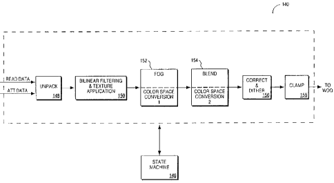
The present invention is implemented in circuitry within stage
2 circuitry 140. Figure 4 illustrates stage 2 circuitry 140 in greater detail.
Stage 2 circuitry 140 implements a pixel pipeline in which the
following functipns are performed: pixel unpacking, bilinear filtering
and texture application, fog, blending, color space conversion, pixel
correction and dithering, and clamping. These functions are
coordinated and timed by a state machine 146. According to the
present invention, color space conversion is performed using both fog
circuitry and blend circuitry, rather than providing separate, dedicated
color space conversion circuitry. More specifically, an initial stage of
color space conversion is performed (when requested) by fog circuitry
152, and a final stage of color space conversion is performed using
blend circuitry 154. Circuit 152 can provide either fog effect or a first
stage of color space conversion at a given point and time, but not both.
Similarly, blend/color space conversion circuit 154, which receives
input from circuit 152, can provide either blending or a second stage of
color space conversion at a given point in time.
In stage 2 circuitry 140, an unpack circuit 148 receives pixel color
values from RAM 110 or data cache 106 via signal READ DATA and
receives pixel attribute values via signal ATT DATA. Unpack circuit
148 converts color data into segments of 8 bits. For example, color data
might be provided to the unpack circuit 148 in 16-bit words, each word
consisting of, for example, three five-bit color segments and 1 unused
bit. Accordingly, unpack circuit 148 would convert ("unpack") each
five-bit color segment within each 16-bit word into a separate 8-bit
CA 02249345 1998-09-15
WO 97/34241 PCT/US97/03318
9
color value. "Unpacked" color values are then provided by unpack
circuit 148 to bilinear filtering and texture application circuitry 150.
Circuitry 150 performs functions which may be required to
provide zooming and application of textured surfaces to an image.
Circuitry 150 outputs pixel color values to fog/color space conversion
circuitry 152. Fog/color space conversion circuitry 152 outputs color
values to blend/color space conversion circuitry 154. Circuit 156
receives as input the output of circuit 154 and provides dithering as
well as a correction function.
The correction function is required to compensate for a
potential loss of pixel intensity that would otherwise be inherent in
the present system. Specifically, the pixel engine 140 uses 8-bit color
values to represent an intensity scale of 0 to 256. However, the
maximum binary value that can be represented with 8 bits is 255,
which is only 99.6 % of the maximum allowable intensity value of
256. Since this ratio is less than 1 (i.e., 0.996), a loss of pixel intensity
would result each time a color value is redrawn unless appropriate
correction is provided. Consequently, circuit 156 rescales each
processed color value to avoid such loss in intensity. The details of
this rescaling procedure are described below with reference to Figure 6.
Clamping circuit 158 receives as input the output of circuit 156
and provides both high end and low end limiting of pixel color
values. Pixel color values are then output by clamp circuit 158 to the
write data queue 142.
CA 02249345 1998-09-15
WO 97/34241 PCT/US97/03318
Figure 5A illustrates the inputs and outputs of fog/color space
circuit 152. Circuit 152 receives as input, for each of the red, green, and
blue color components, a destination color value, D c, a source color
value, Tex c, and a fog color value, FogColor_c. (Note that in this
description, the suffix ' -c" in the name of a signal is generic and may
be replaced in the actual circuit by a more specific suffix to indicate that
signal for a particular color component or channel, e.g., ' _r" for the
red channel.) In addition, circuit 152 receives as input a fog factor,
FogMult. Further, circuit 152 receives from state machine 146 control
signals YLTV2RGB and PASS. Circuit 152 outputs the destination color
value D_c and a modified source color value S_c for reach of the red,
green, and blue color components. In addition, circuit 152 outputs an
intermediate color signal sY, which is used during color space
conversion, as will be described below.
Circuit 152 can be placed in either fog mode or color space
conversion mode according to the state of control signal YUV2RGB.
Specifically, circuit 152 performs color space conversion when signal
YLTV2RGB is asserted. In the preferred embodiment, signal
YUV2RGB is an active-high signal.
In the preferred embodiment, the color space conversion
function converts color values in YCr Cb (luminance, red
chrominance, blue chrominance) color space, sometimes referred to as
YUV color space, to color values in RGB (red, green, blue) color space.
It should be appreciated, however, that color space conversion may be
CA 02249345 1998-09-15
WO 97/34241 PCT/US97/03318
11
performed between various different color spaces other than YCrCb or
RGB within the scope of the present invention.
Control signal PASS will be asserted when neither color space
conversion nor fog effect is requested. The effect of asserting the PASS
signal is to cause the source color value Tex c to be passed through
circuit 152 to output S_c unmodified.
In fog mode (i.e., when signal YLJV2RGB is not asserted), circuit
152 generally modifies the input source color value Tex_c based on
the following well-known fog equation:
S_c = FogMult * (Tex_c - FogColor_c) + FogColor ( 1 )
More specifically, however, circuit 152 actually implements equation
(2) in order to provide proper rounding of color values.
S_c = [FogMult * (Tex_c - FogColor_c) + ((FogColor_c« 8) + 128))»8 (2)
The symbols "«" and "»" represent the functions "shift left"
and "shift right", respectively, where the number immediately
following the symbol indicates the number of bits by which the
number immediately preceding the symbol is to be shifted.
As noted above, the present system uses a pixel intensity scale
of 0 to 256. Hence, adding the value 128 in equation (2) has the effect
of adding one half (i.e., 128/256 = 0.5) to the partial sum which
precedes it. In equation {2), and in the circuitry which implements
CA 02249345 1998-09-15
WO 97/34241 PCT/US97/03318
12
equation (2), adding the value 128 to the partial sum and then right-
shifting the resulting sum by eight bits ensures proper rounding of
pixel color values.
In color space conversion mode (i.e., when signal YUV2RGB is
asserted), circuit 152 generates intermediate term sY based, in concept,
on equation (3), where Y represents the input luminance value.
sY = 1.16 * (Y - 0.063) + 0.5 (3)
However, because the present system uses a color value
intensity scale of 0 to 256, circuit I52 actually generates signal sY
according to equation (4), where the values 297, 16, and 128 are based
on a scale of fl to 256.
sY = 297 * (Y -16) + 128 (4}
The luminance value Y is applied to the Tex c input of the
green component circuit of circuit 152 (i.e., to the Text input) during
color space conversion, as will be described below.
Figure 5B illustrates the inputs and outputs of blend/color space
conversion circuit 154. Circuit 154 performs either blending or a
second stage of the color space conversion, depending on the state of
control signal YUV2RGB. Specifically, color space conversion is
performed when signal YUV2RGB is asserted. Circuit 154 receives as
inputs, for each of the red, green, and blue color components, signals
CA 02249345 1998-09-15
WO 97/34241 PCT/US97/03318
13
S_c and D_c. Destination color values D_c are received from frame
buffer 112. In addition, circuit 154 receives signals BlendSrc and
BlendDst, and sY. In blend mode, circuit 154 generates an output color
value P_c according to equation (5).
P_c = S_c * BlendSrc + D c * BlendDst (5)
Blend equation (5) is well known in the art of computer
graphics. In equation (5), as is well known, the value BlendSrc can
have the following possible values: D_c, 1 - D_c, S_alpha, 1 - S alpha,
D_alpha, 1 - D_alpha, 0, 1, source_aipha saturate, or 1 - source-alpha-
saturate. In the aforementioned signals, "alpha" refers to the
transparency channel (attribute). The alpha channel and the nature of
its associated signals named above are well-known in the art of
designing graphics processing circuitry. The details of the alpha
channel and methods of generating these signals are not necessary to
understanding of the present invention and are therefore not
discussed herein.
Similarly, BiendDst can have the following possible value: S_c,
1 - S_c, S_alpha, 1 - S_alpha, D alpha, 1 - D alpha, 0, or 1. In addition
to control signal YWZRGB, circuit 154 receives the following 3-bit
control signals: BlendSrcSel, BlendSrcCompl, BlendDstSel, and
Blend~stCompl. These control signals are used to select values for
BlendSrc and BlendDst.
CA 02249345 1998-09-15
WO 97/34241 PCT/LTS97/03318
14
The output of circuit 154, pixel color value P_c, is provided to
correction and dither circuit 156, which performs correction as
described above and which provides dithering in accordance with a
dither matrix value. Procedures for performing dithering are well
known in the art and accordingly need not be described herein.
Correction and dither circuit 156 provides an output color value P _c
to clamping circuit 158 for each of the red, green, and blue color
components.
During color space conversion (i.e., when signal YUV2RGB is
asserted), circuits 152 and 154, in combination, generate red (R), green
(G), and blue (B) color values based, in concept, on equations (6), (7),
and (8), using sY as defined by equation (3), where Cr and Cb represent
red and blue chrominance values, respectively.
R = sY + 1.590 * (Cr - 0.5) (6)
G = sY - 0.806 * (Cr - 0.5) - 0.391 * {Cb - 0.5) (7)
B=sY+2.011 *(Cb-0.5) (8)
However, because the present system uses an intensity scale of 0
to 256, circuit 154 actually generates red, green, and blue pixel color
values P_r, Pte, and P b, respectively, according to equations (9), (10),
and (11), where sY is defined by equation (4).
P_r = floor((sY + 407 * (Cr - 128)) / 255) (9)
P~ = floor((sY - 207 * (Cr -128) -100 * (Cb -128)) / 255) (10)
CA 02249345 1998-09-15
WO 97/34241 PCT/US97/03318
P b = floor((sY + 515 * (Cb -128)) / 255) (11)
During color space conversion, the fog color inputs FogColor_c
to circuit 152 must be set to the following values (based on a scale of 0
to 256) for the red, green, and blue components, respectively:
FogColor_r = 128; FogColor~ = 16; and FogColor_b = 128.
Referring now to Figure 7, fog/color space circuit 152 is
illustrated in greater detail. It should be appreciated that fog equations
(1) and (2) are, in general, linear interpolation functions having the
general format, output = F * (B - A) + A + 1/2. It should also be
appreciated that the color space conversion equations (9) through (11)
can also be expressed in this same general format. The present
invention therefore takes advantage of this fact in order to use the fog
circuitry and blend circuitry to perform color space conversion.
As shown in Figure 7, circuitry 152 contains separate
component circuits 152a, 152b, and 152c, for each of the red, green, and
blue color components, respectively. The red color component
circuitry 152a includes a subtractor 160, a multiplier 162, an adder 164,
multiplexors 166 and 168, and registers 170 and 172. To implement
either the fog or color conversion functions described above, these
elements are coupled as follows: Subtractor 160 receives the red
source color value Tex_r as a first input and the red fog color value
FogColor_r as a second input and outputs a difference of those two
signals, d_r. Tex_r and FogColor_r are each unsigned 8-bit numbers,
while output D_r is a signed 9-bit number. Multiplier 162 receives as
CA 02249345 1998-09-15
WO 9?/34241 PCT/ITS97/03318
16
a first input the signal d_r and receives as a second input the fog factor
FogMult, which is an 8-bit unsigned number. The multiplier 162
outputs the product of its two inputs as a signed 17-bit number to a
first input of adder 164. The second input of adder 164 receives a 16-bit
number, the eight least significant bits (LSBs) of which are set to the
value 128, and the eight most significant bits (MSBs) of which are
provided by the signal FogColor_r. Adder 164 generates an 18-bit sum
(bits 0 through 17), bits 8 through 15 of which are output to input 0 of
multiplexor 168.
Multiplexor 168 is a three-input multiplexor. Input 1 of
multiplexor 168 receives signal D r, while input 2 of input
multiplexor 168 receives Tex_r. The inputs of multiplexor 168 are
selected according to the combination of signals PASS and YLTV2RGB,
which are applied to control inputs s1 and s0, respectively, of
multiplexor 168. In particular, if PASS is set to 1, then input 2 of
multiplexor 168 is passed through to its output to register 172.
Otherwise, if YUV2RGB is 0, then input 0 is selected, and if YUV2RGB
is 1, input 1 is selected.
Multiplexor 166 is a two input multiplexor. Input 0 which
receives the red destination color value D_r, while input 1 receives
signal d_R. The inputs are selected according to the state of signal
YLTV2RGB, as described above, which is applied to the control input s
of multiplexor 166. The output of multiplexor 166 is supplied to
register 170. The output of register 170 is the signal D r, and the
CA 02249345 1998-09-15
WO 97/34241 PCT/US97/03318
17
output of register 172 is signal S_r, each of which is a signed 9-bit
number.
When signal YLTV2RGB is asserted (i.e., when color space
conversion is requested), then the Tex_r input receives the Cr value,
and the FogColor_r input is set to 128. During color space conversion,
the signal FogMult is used only by the green component circuit, as
described below.
It should be appreciated that by using the circuit configuration
illustrated in Figure 7 and described above, the output S_r of circuit
152 will have the value Cr - 128 during color space conversion (note
that input 1 of multiplexor 168 will be selected).
Fog/color space conversion circuit 152 also includes green
component circuitry 152b comprising subtractor 180, multiplier 182,
adder 184, multiplexors 186, 188, 194,196, 198, and registers 190,192,
and 200. Registers 190 and 192 output signals D~ and Sue, each as a
signed 9-bit number. Register 200 outputs intermediate color signal sY
as a signed 18-bit number during color space conversion. Subtractor .
180 receives input signals Text and FogColor_g, each as an unsigned
8-bit number and generates a difference signal d~ as a signed 9-bit
number. Signal d~ is applied to one input of multiplier 182, while a
second input of multiplier 182 is received as the output of multiplier
194. Multiplier 182 generates a signed 17-bit output which is applied to
one input of adder I84. A second input of adder 184 receives a 16-bit
number, the eight LSBs of which are set to 128, while the eight MSBs
of which are provided as the output of multiplex 196. The output of
CA 02249345 1998-09-15
WO 97/34241 PCT/US97/03318
18
adder 184 is an 18-bit sum signal which is applied to the zero input of
multiplexor 188.
Multiplexor 188 is a three-input multiplexor which is
controlled using signal PASS and YW2RGB in the manner described
above with respect to the red component circuitry. Similarly,
multiplexor 186 is a two-input multiplexor controlled by signal
YLTV2RGB, as described above. Input 0 of multiplexor 186 receives
signal Due, while input 1 of multiplexor 186 receives the output of
subtractor 210 of the blue component circuit, as will be described
below. Input 1 of multiplexor 188 receives signal d_r from the red
component circuit 152a, while the two input receives signal Text.
Multiplexors 194 and 196 are each two-input multiplexors controlled
by signal YLTV2RGB. A value of 41 is applied to input 1 of mulHplexor
194, while the signal FogMult is applied to input 0 of multiplexor 194.
Input 1 of multiplexor 196 receives the output d~ of subtractor 180,
while input 0 of multiplexor 196 receives the signal FogCoior~.
Multiplexor 198 is a two-input multiplexor controlled by signal
YW2RGB. Input 1 of multiplexor 198 receives the output of adder
184, while input 0 of multiplexor 198 receives the value of 128.
During color space conversion (when signal YUV2RGB is set to
1), the Text input receives the luminance value Y, while the
FogColor~ input receives the value 16. The Fog factor FogMult is set
to a value of 41. It should be appreciated that the intermediate signal
sY is used only during color space conversion. It should further be
appreciated that during color space conversion, the output S~ of
CA 02249345 1998-09-15
WO 97/34241 PCT/US97/03318
19
register 192 has the value Cr - 128, while the signal D~ has the value
Cb - 128. Note that, during color space conversion, the second input
of adder 184 receives a signal having the value 256 * (Y - 16), which is
the combination .of the output of multiplexor 196 and the value 128.
More specifically, the value Y - 16 is provided through input 1 of
multiplexor 196, which value is then multiplied by 256 by shifting the
value eight bits to the left. The eight LSBs bits of the resulting 16-bit
number are then set to 128 to provide proper rounding.
Circuit 152 also contains blue component circuitry 152c
including subtractor 210, multiplier 212, adder 214, multiplexors 216
and 218, and registers 220 and 222. Register 220 outputs signal d b as a
signed 9-bit number, while register 222 outputs signal S_b as an
unsigned 9-bit number. Subtractor 210 receives signal Tex b as an
unsigned 8-bit number at a first input and signal FogColor_b as an
unsigned 8 bit number at second input and outputs the difference of
those two signals as signal d b, a signed 9-bit number. Signal d b is
provided to one input of multiplier 212, while the other input of
multiplier 212 receives the fog factor signal, FogMult. Multiplier 212
outputs the product of its two inputs as a signed 17 bit number, which
is applied to one input of adder 214. The other input of adder 214
receives a 16-bit number, the eight LSBs of which are set to 128, and
the eight MSBs of which are formed by the signal FogColor_b. Adder
214 outputs a signed' 18-bit number to input 0 of multiplexor 218.
Multiplexor 218 is a three-input multiplexor controlled by the
combination of signals PASS and YL1V2RGB in the manner described
CA 02249345 1998-09-15
WO 97/34241 PCT/US97/03318
above. Input 1 of multiplexor 218 receives the output d b of
subtractor 210. Input 2 of multiplexor 218 receives signal Tex b.
Multiplexor 218 provides its output to the input of register 222.
Multiplexor 216 is a two-input multiplexor controlled by signal
YW2RGB applied to its control input s. Input 0 of multiplexor 2I6
receives signal D b, while input 1 of multiplexor 216 receives
difference signal d b.
During color space conversion, input Tex_b receives the Cb
value, while the FogColor_b input receives the value 128.
Accordingly, it will be appreciated that during color space conversion,
output S_b is equal to outputs D b and D_g, which have the value Cb
- 128. Accordingly, during color space conversion, signals D_r, S_r,
D_g, Sue, sY, D b, and S b are provided to blend/color space
conversion circuit 154 for the second (final) stage of color space
conversion.
Figures SA, 8B, and 8C illustrate blend/color space conversion
circuit 154 and correcHon/dither circuit 156 in greater detail. In
particular, circuits 154 and 156 includes red component circuitry 154a
and 156a, respectively (Figure 8A); green component circuitry 154b and
156b, respectively (Figure 8B); and blue component circuitry 154c and
156c, respectively (Figure 8C).
Referring now to Figure 8A, the red component circuitry 154a of
circuit 154 includes multiplexors 250, 252, 258, and 262, exclusive OR
(XOR) gates 252 and 260, multipliers 256 and 264, and adder 266.
Multiplier 256 receives signal S_r from circuit 152 as a signed 9-bit
CA 02249345 1998-09-15
WO 97/34241 PCT/I1S97/03318
21
number at one input and the output of multiplexor 254 as an
unsigned 8-bit number at a second input. Multiplexor 254 is a two-
input multiplexor controlled by signal YUV2RGB applied to its
control input s. Input 0 of multiplexor 254 receives the output of XOR
gate 252, while input 1 of multiplexor 254 (used during color space
conversion) receives the value 152. XOR gate 252 has two inputs, one
of which receives the output of multiplexor 250 while the other
receives the LSB (bit 0) of signal BlendSrcCompl.
Multiplexor 250 is a two-input multiplexor controlled by signal
BlendSrcSe1 applied to its control input s. Input 0 of multiplexor 250
receives signal BlendSrc while input 1 receives signal D_r from circuit
152. The output of multiplier 256 is applied to input 1 of three-input
adder 266. A second input ~of adder 266 receives intermediate signal sY
from circuit 152 as a signed 18-bit number. Note that during blending,
(i.e., when signal YLTV2RGB is not asserted), signal sY is set to 128 to
facilitate proper rounding. The third input of adder 266 receives the
output of multiplier 264. Multiplier 264 receives as input the signed 9-
bit signal D_r from circuit 152 and the unsigned 8-bit output of
multiplexor 262.
Multiplexor 262 is a two-input multiplexor controlled by signal
YW2RGB. Input 0 of multiplexor 262 receives the output of XOR
gate 260, while input 1 receives the value 255. XOR gate 260 receives
the output of multiplexor 258 at a first input and the LSB (bit 0) of
signal BlendSrcCompl at second input. Multiplexor 258 is a two-input
multiplexor controlled by signal BlendDstSel. Input 0 of multiplexor
CA 02249345 1998-09-15
WO 97/34241 PCT/US97/03318
22
258 receives signal BlendDst, while input 1 of multiplexor 258 receives
signal S_r from circuit 152. Adder 266 outputs a signed 19-bit signal
P_r. It will be appreciated that during color space conversion, signal
P_r is generated according to the equation {9).
Signal BlendSrc may have any of the following possible values:
source-alpha-saturate, S_alpha, D alpha, and 00; the value at any
given time is determined by the value of three-bit control signal
BlendSrcCompl. In particular, the two MSBs (bits 1 and 2) of signal
BlendSrcCompl are used to select the value of BlendSrc. This
function may be accomplished by applying the possible values of
BlendSrc as inputs to a multiplexor (not shown) and using signal
BlendSrcCompl as the control input of the multiplexor. Similarly,
signal BlendDst may have any of the values, D alpha, 00, S_alpha, as
determined by the value of the two MSBs of signal BlendDstCompl.
XOR gates 252 and 260 provide a selectable inversion function.
That is, signals BlendSrcCompl and BlendDstCompl are applied as
control signals to one input of XOR gates 252 and 260, respectively.
When asserted, the control signal causes the other input of the XOR
gate to be inverted. When the control signal is not asserted, the other
input of the XOR gate is effectively passed through to the output.
Hence, this inversion function can be used during blending to derive
additional values from the signals BlendSrc and BlendDst, namely the
values (1 - BlendSrc) and (1 - BlendDst).
Referring now to Figure 8B, circuit 154 also includes green color
component circuitry 154b. The green component circuitry 154b of
CA 02249345 1998-09-15
WO 97/34241 PCT/US97/03318
23
circuit 154 includes multiplexors 300, 304, 310, and 314, XOR gates 302
and 312, multipliers 306 and 316, and adder 308. Circuit 154b has a
structure that is essentially identical to that of circuit 154a. In
particular, multiplier 306 receives signal S~ from circuit 152 as a
signed 9-bit number at one input and the output of multiplexor 304 as
an unsigned 8-bit number at a second input. Multiplexor 304 is a two-
input multiplexor controlled by signal YW2RGB applied to its
control input s. Input 0 of multiplexor 304 receives the output of XOR
gate 302, while input 1 of multiplexor 304 (used during color space
conversion) receives the value -207. XOR gate 302 has two inputs, one
of which receives the output of multiplexor 300 while the other
receives the LSB (bit 0) of signal BlendSrcCompl. XOR gates 302 and
312 provide a selectable inversion function, as described above with
reference to XOR gates 252 and 260.
Multiplexor 300 is a two-input multiplexor controlled by signal
BlendSrcSe1 applied to its control input s. Input 0 of multiplexor 300
receives signal BlendSrc while input 1 receives signal D~ from circuit
152. The output of multiplier 306 is applied to input 1 of three-input
adder 308. A second input of adder 308 receives intermediate signal sY
from circuit 152 as a signed 18-bit number. As mentioned above,
signal sY is set to 128 during blending to provide proper rounding.
The third input of adder 308 receives the output of multiplier 316.
Multiplier 316 receives as input the signed 9-bit signal D~ from
circuit 152 and the unsigned 8-bit output of multiplexor 314.
CA 02249345 1998-09-15
WO 97/34241 PCTIUS97/03318
24
Multiplexor 314 is a two-input multiplexor controlled by signal
YLTV2RGB. Input 0 of multiplexor 314 receives the output of XOR
gate 312, while input 1 receives the value -100. XOR gate 312 receives
the output of multiplexor 310 at a first input and the LSB (bit 0) of
signal BlendDstCompl at a second input. Multiplexor 310 is a two-
input multiplexor controlled by signal BlendDstSel. Input 0 of
multiplexor 310 receives signal BlendDst, while input 1 of multiplexor
310 receives signal S_r from circuit 152. Adder 308 outputs a signed
19-bit signal P,~. It will be appreciated that during color space
conversion, signal P~ is generated according to the equation (10).
Referring now to Figure 8C, circuit 154 also includes blue color
component circuitry 154c. The blue component circuitry 154c of circuit
154 includes multiplexors 340, 358, 346, 350, and 352, XOR gates 342 and
348, multipliers 344 and 354, and adder 356. Circuit 154c has a
structure that is similar to that of circuits 154a and 154b. In particular,
multiplier 344 receives signal S_b from circuit 152 as a signed 9-bit
number at one input and the output of multiplexor 358 as an
unsigned 8-bit number at a second input. Multiplexor 358 is a two-
input multiplexor controlled by signal YL1V2RGB applied to its
control input s. Input 0 of multiplexor 358 receives the output of XOR
gate 342, while input 1 of multiplexor 358 (used during color space
conversion) receives the value 131. XOR gate 342 has two inputs, one
of which receives the output of multiplexor 340 while the other
receives the LSB (bit 0) of signal BlendSrcCompl. XOR gates 342 and
CA 02249345 1998-09-15
WO 97/34241 PCT/US97/03318
348 provide a selectable inversion function, as described above with
reference to XOR gates 252 and 260.
Multiplexor 340 is a two-input multiplexor controlled by signal
BlendSrcSel applied to its control input s. Input 0 of multiplexor 340
receives signal BlendSrc while input 1 receives signal D b from circuit
152. The output of multiplier 344 is applied to a first input of four-
input adder 356. A second input of adder 356 receives intermediate
signal sY as a signed 18-bit number from circuit 152. Again, signal sY
is set to 128 during blending. A third input of adder 356 receives the
output of multiplier 354. Multiplier 354 receives as input the signed 9-
bit signal D_b from circuit 152 and the unsigned 8-bit output of
multiplexor 350. The fourth input of adder 356 receives the output of
multipiexor 352. Multiplexor 352 has two inputs and is controlled by
signal YLTV2RGB applied to its control input s. A first input of
multiplexor 352, which is selected when signal YLTV2RGB is not
asserted, receives the value 0. The second input of multiplexor 352
receives the value D b«8 (D b left-shifted by eight bits).
Multiplexor 350 is a two-input multiplexor controlled by signal
YLTV2RGB. Input 0 of multiplexor 350 receives the output of XOR
gate 348, while input 1 receives the value 128. XOR gate 348 receives
the output of multiplexor 346 at a first input and the LSB {bit 0) of
signal BlendDstCompl at a second input. Multiplexor 346 is a two-
input multiplexor controlled by signal BlendDstSel. Input 0 of
multiplexor 346 receives signal BlendDst, while input 1 of multiplexor
34b receives signal S_r from circuit 152. Adder 356 outputs a signed
CA 02249345 1998-09-15
WO 97/34241 PCT/US97/03318
26
19-bit signal P_g. It should be appreciated that during color space
conversion, signal P~ is generated according to the equation (11).
In circuit 154c (Figure 8C), the values 131, 128, and D b « 8
applied to multiplexors 358, 350, and 352, respectively, represent in
combination the factor 515 in equation (11). That is, (131 + 128) * D b
+ (D b « 8) _ (131 + 128 + 256) * D b = 515 * D b, which equals 515 *
(Cr - 128) during color space conversion.
Hence, it should be appreciated that during color space
conversion mode (i.e., when signal YLTV2RGB is asserted), circuit 152
in combination with circuits 154a, 154b, and 154c implement equations
(9) through (11).
Color signals P_r, P_g, and P b are applied to correction and
dither circuit 156, and more precise:y, to subcircuits 156a, 156b, and
156c, respectively. Correction and dither circuit 156 simultaneously
performs dithering and scaling of the value of signal P r in the
manner described above. Correction and dither circuit 156 includes a
single full adder 270. Adder 270 has two inputs, each of which
receives a 16-bit number. The principle of operation of dither and
correction circuit 156 will now be described with reference to Figures
6A, 6B, and 6C.
Figure 6A illustrates a correction function for scaling color
values to a scale of 0 to 256. Assume that an input pixel color value is
initially received by a correction circuit as a 16-bit value P_c including
a fractional component. The color value P_c is added to a second
value, which consists of the value P c shifted right by eight bits.
CA 02249345 1998-09-15
WO 97/34241 PCT/US97/03318
27
Hence, in the second value, the lowest eight bits are discarded. The
resulting sum is a 16-bit number, the lowest eight bits of which are
also discarded. The remaining eight bits represent a "corrected" pixel
value P _c, which is correctly scaled such that the maximum possible
value corresponds to the maximum possible intensity.
Figure 6B illustrates an example of a dithering function. An 8-
bit dither value DVaI_c is used to operate upon the pixel color value
P_c. The dither value DVaI c is the dither matrix value appropriately
shifted based on the number of bits used to represent color values in
memory. The steps for generating a dither matrix are well-known in
the art of computer graphics and accordingly will not be discussed
herein. The &bit dither value DVaI c is padded with eight zeros on
the right and then added to' the 16-bit pixel colcr value P_c. In the
resulting sum, the eight LSBs are discarded and the remaining bits are
taken as the dithered color value P' c.
In accordance with the present invention, dithering and
correction are performed simultaneously by 156a, 156b, and 156c for
the red, green, and blue color components, as illustrated in Figure 6C.
Referring now to Figure 6C and, for example, to Figure 8A, the 8-bit
dither value DVal_r is padded on the right with the eight MSBs of a
pixel value P r to form a 16-bit compound value which is received at
one input of adder 270. This 16-bit compound value is then added to
the lowest 16 bits of color value P_r (a 19-bit value), which is applied
to the second input of adder 270. The eight LSBs of the resulting sum
are discarded, such that the remaining eight bits form the corrected
CA 02249345 1998-09-15
WO 97/34241 PCT/US97/03318
28
and dithered color value Corr_r. The color value Con r is corrected
to a scale of 0 to 256. Essentially the same function is performed in
circuits 156b and 156c to generate signals Corr_g and Corr-b,
respectively.
Hence, each of correction and dither circuits 156a, 156b, and 156c
outputs a corrected pixel color value Corr_c and a carry out signal to
clamping circuit 158. In addition, clamping circuit 158 is supplied with
the three MSBs of the P_c signals.
Thus, a method and apparatus for performing color space
conversion using blend logic have been described. Although the
present invention has been described with reference to specific
exemplary embodiments, it will be evident that various modifications
and changes may be made to these embodiments without departing
from the broader spirit and scope of the invention as set forth in the
claims. Accordingly, the specification and drawings are to be regarded
in an illustrative rather than a restrictive sense.