Note: Descriptions are shown in the official language in which they were submitted.
RD-25,964
CA 02249856 1998-10-08
.1.
FIVE LEVEL HIGH POWER MOTOR DRIVE
CONVERTER AND CONTROL SYSTEM
BACKGROUND OF THE INVENTION
The present invention relates generally to three phase power converters used
in high power motor drive systems. The invention relates more specifically to
a fast
response five level power inverter circuit capable of medium voltage operation
without
series connection of power electronic switching devices and to an associated
modulation control for determining gate timings for the power electronic
switching
devices.
Baker et al., US Patent No. 4,270,163, and others have proposed generalized
inverter power circuits having four or more levels. This proposed mufti-level
converter
configuration, when used in a five level embodiment, has multiple practical
issues
impeding construction of a converter system including: twice the direct
current (DC)
bus voltage of this invention, difficulties obtaining practical high speed
clamp diodes
(clamp diodes require higher blocking voltages than the switching devices),
complicated capacitor balancing requirements, and long convoluted inductive
circuit
commutation paths.
SUMMARY OF THE INVENTION
It would be desirable to provide a power inverter circuit which has reduced
bus voltage requirements and a simpler circuit topology and which acts as a
low total
harmonic distortion iTHD) IEEE-519 compliant power grid interface.
More specifically, it would also to be desirable to provide a quick response
2 0 high power motor drive converter system in the 1+ MW range capable of
supplying an
AC drive motor with medium voltage output 3.3-4.16 KV at fundamental output
frequencies up into the 100-200 Hz range.
In an embodiment of the present invention, a quick response high power
motor drive converter system includes: a five level hybrid NPC output power
2 5 conversion stage connected to an AC drive motor, three isolated split
series
connected DC capacitor banks, a controller for computing switch timings with
active
control of neutral voltages, a rectifier transformer with three isolated sets
of twenty
degree phase shifted five level secondaries, and three diode rectifier source
converter
bridges.
3 0 The hybrid NPC output power converter stage and three isolated DC busses
create a five level power converter which minimizes voltage steps applied to
the drive
motor and thereby reduces winding stresses. The five level converter also
enables
RD-2s,ssa
CA 02249856 1998-10-08
.2_
creation of the medium voltage output levels using commercially available
switching
devices (e.g. insulated gate bipolar transistors).
The modulator control of the five level inverter is used to determine the gate
timings for the power electronic switches in the three phase power converter.
The
converter, in general, produces sinusoidal voltage and currents by a pulse
width
modulation process in order to achieve smooth control over load voltage. The
converter modulation control should be capable of operating as the actuation
stage in
a vector controlled induction or synchronous motor control and thus be able to
create
an arbitrary output voltage vector at each control sampling instant in
response to
transient torque events. The modulation control is preferably software based
to
minimize any specialized hardware requirements. The modulator control provides
compensation for the significant ripple voltages on the independent power
converter
busses.
This embodiment will support a variety of options including the addition of
actively controlling dynamic braking resistors, capacitor bleed/balance
resistors,
snubber circuits on the inner switch elements and/or on the outer switch
elements.
Another modification includes of the addition of a neutral-ground reference
network
tuned to provide damping for reflected wavefronts propagating on the motor
cables.
.BRIEF DESCRIPTION OF THE DRAWINGS
2 0 The features of the invention believed to be novel are set forth with
particularity in the appended claims. The invention itself, however, both as
to
organization and method of operation, together with further objects and
advantages
thereof, may best be understood by reference to the following description
taken in
conjunction with the accompanying drawings, where like numerals represent like
2 5 components, in which:
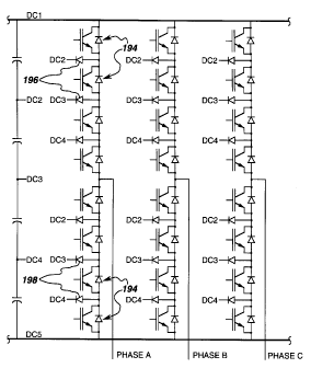
FIG. 1 is a cirouit diagram of a multi-level embodiment.
FIG. 2 is a circuit diagram of a single phase bridge of a five level inverter.
FIG. 3 is a circuit diagram of a NPC three level phase leg.
FIG. 4 is a circuit diagram of snubber circuits applied to inner sw'ttch
elements
3 0 of the NPC phase leg of FIG. 3.
FIG. 5 is a circuit diagram of snubber circuits applied to outer switch
elements
of the NPC phase leg of FIG. 3.
FIG. 6 is a circuit diagram of a single phase bridge of five level inverter
with a
dynamic braking (DB) circuit.
3 5 FIG. 7 is a circuit diagram of a low total harmonic distortion (THD) five
level
inverter circuit with isolated DC busses.
FIG. 8 is a diagram of five level modulation control.
RD-25,964
CA 02249856 1998-10-08
-3-
FIG. 9 is a graph of sine-triangle modulation control with DC bus feedforvvard
and third Harmonic Injection.
FIG.10 is a graph of a line-neutral voltage switching pattern.
FIG. 11 is a graph of a line-line voltage switching pattern.
FIG.12 is a graph illustrating 'space vector' equivalent ham~onic injection.
FIG.13 is a graph of a zero-sequence injection pattern for Vref < Y~Vdc.
FIG.14 is a graph of a zero-sequence injection pattern for l/2Vdc < Vref <
Vdc.
F1G.15 is a graph of a zero-sequence injection pattern for Vdc < Vref < 3/2
Vdc.
FIG. 16 is a graph of a discontinuous modulation injection pattern.
FIG.17 is a graph of a simulated grid current.
FIG.18 is a graph of a simulated load current.
DETAILED DESCRIPTION OF A PREFERRED EMBODIMENT OF THE
INVENTION
Aforementioned Baker et al., US Patent No. 4,270,163, proposed generalized
inverter power circuits having four or more levels. FIG. 1 is an application
of the
Baker et al. proposal to a five level inverter. Baker states that a polyphase
output
voltage of greater than three phases can be provided by adding additional
upper and
lower legs with switches (shown in FIG. 1 as switch diode pairs 194) and clamp
2 0 diodes (shown in FIG. 1 as diodes 196 and 198). Baker states that each new
upper
and lower leg so added to the three phase embodiment provides an additional
phase,
and that adding the diodes and switches can also permit higher levels of DC
voltage
to be converted into higher amplitude AC output wavefom~s.
FIG. 2 is a circuit diagram of a single phase bridge 100 of a five level
inverter
110 (shown in FIG. 7) which combines two NPC (neutral point clamped) three
level
phase legs 118 with a common DC bus (with a positive rail 120,a negative rail
124,
and a midpoint 126) to provide an NPC H-bridge. The NPC three level phase legs
include electrical switches 114 which are shown as IGBTs (Insulated Gate
Bipolar
Transistors). Other useful switches include GTOs (Gate Tum Off Thyristors) and
3 0 IGCTs (Integrated Gate Commutated Thyristors). The switches are paired
with anti-
parallel freewheeling diodes 116 to accommodate the inductive motor load
currents.
A controller 15 is used for controlling each of the switches. The controller
may
comprise, for example, a computer, a microcomputer, a microprocessor, or, in a
preferred embodiment, a digital signal processor.
3 5 FIG. 3 is a circuit diagram of an individual NPC three level phase leg 118
of
FIG. 2. The three phase inverter has four switch and diode pairs spanning the
DC
CA 02249856 1998-10-08
R D-25.964
-4-
bus and two clamping diodes 122 (labeled D5, D6). The sw'ttch diode pairs are
labeled top to bottom S1/D1, S2/D2, S3/D3, S4/D4. As shown in Table 1, there
are
three command states for the switches per phase leg.
STATE 1 S1 ON S2 S3 S4 OFF LOAD PT ~ P-BUS
(+) ON OFF
STATE 2 S1 OFF S2 S3 S4 OFF LOAD PT ~P MID-POINT
(0) ON ON
STATE 3 S1 OFF S2 S3 S4 ON LOAD PT ~ N-BUS
(-) OFF ON
e 1 tates
Tabl NPC
S
Depending on the switch commanded state per phase, and the instantaneous
polarity of the load current in that phase, the load current path can be
through
switches, freewheeling diodes, or clamping diodes. For example, if the
commanded
state is STATE 2, and the load current is positive, the load current path is
through
clamp diode D5 and switch S2. If the commanded state is STATE 2, and the load
current is negative, the load current path is through switch S3, and clamp
diode D6.
Table 1 shows the load terminal per phase can be either at P-bus, N-bus, or
DC bus midpoint, which gives rise to the terminology three level or neutral
point
clamped inverter. In a two level inverter, the load terminal per phase is
either at P-bus
or N-bus. This extra load point level, that is, the DC midpoint, in the three
level
inverter accounts for its lower load current harmonic amplitudes than a two
level
inverter chopping at the same frequency.
The capacitor 128 bank 130 midpoint (at DC midpoint 126) and the clamping
2 0 diodes 122 connected between capacitor bank midpoint and switches S1/S2
and
S3/S4 respectively keep the maximum DC working voltage across any switch from
exceeding one half of the DC bus voltage (Vdc/2), provided the DC filter
capac'ttor
midpoint voltage is maintained at Vdcl2. Regulators are built into the
modulator to
keep the midpoint voltage at Vdc/2 to guard against long term unequal
discharge of
2 5 the two capacitor bank halves. The resistor network 119 (shown in FIG. 2)
across the
DC bus capacitor bank serves as a fixed safety bleed resistor and a balance
network
for initial capacitor charging.
FIG. 4 is a circuit diagram of optional snubber circuits 132 applied to inner
switches 114a of the NPC phase leg of FIG. 3. A snubber diode 134 will turn on
3 0 during switch turn-off whenever the voltage across the device exceeds the
positive
portion 120 of the bus, effectively placing the snubber capacitor 136 in
parallel with
switch 114a. The capacitor will transiently absorb the excess energy stored in
the
parasitic circuit inductances in series with the switch. After the switch is
turned off, the
ringup voltage across the snubber capacitor is dissipated in the snubber
resistor 138.
3 5 The snubber elements are sized to keep the switching trajectory of voltage
and
RD-25,964
CA 02249856 1998-10-08
-5-
current within the a safe operating area. If IGBT switches are used, an
inverter will
typically be constructed with low inductance circuit paths and buswork so that
at low
current levels the phase leg can be safely switched. The inner switches 114a
(S2 8~
S3) commutate current between higher inductance circuit paths as compared to
outer
switches 114b (S1 & S4) with current switching through four device elements
rather
than two device elements. Consequently, the inner switches will experience
greater
voltage overrings and can require snubbers.
FIG. 5 is a circuit diagram of optional snubber circuits applied to outer
switches of the NPC phase leg of FIG. 4. The illustrated outer switch snubbers
also
act to clamp the overring across the switch to half the DC bus voltage during
device
turnoff. Snubber diode 142, snubber capacitor 144, and snubber resistor 146 of
FIG.
4 operate on the outer switches in the same manner as snubber diode 134,
snubber
capacitor 136, and snubber resistor 138 of FIG. 4 operate on the inner
switches.
In the circuit of FIG. 2, if one phase of the load (line-neutral) is connected
across the bridge, the output voltage can have three levels in each polarity:
0, VdcJ2,
and Vdc, where Vdc is the DC bus voltage. This permits a total of five unique
voltage
levels to be generated across the load as shown in Table 3. The phase bridge
states
are labeled M-Q in five levels with M being the most negative and D most
positive.
Phase-BridgePhase-Leg Phase-Leg Phase-Bridge
State A1 State A2 State Voltage
M + - -Vdc
+ 0
N 0 - -Vdc/2
+ +
O 0 0 0
P 0 + +VdG2
- 0
Q - + +Vdc
Table 3 five level Bridge States
States M and Q are unique, and, because neither the A1 nor A2 phase legs are
in the
0 state, the charge balance between the upper and lower halves of the DC
capacitor
2 5 bank is not forced to change.
States N and P will affect the charge balance between the upper and lower
half of the DC bus capacitor bank because only one of the two NPC phase legs
is
R D-25 , 964
CA 02249856 1998-10-08
-6-
connected in the 0 state. Depending on which of the redundant connections are
selected for state N (or P) and load current polarity, the load current will
either directly
charge or discharge the DC bus neutral point. By controlling the relative
dwell time
between these two alternative N (or P) connections the modulation algorithm
can
actively control the neutral voltage balance.
State O is also not unique, producing zero voltage across the bridge output by
either of three alternative phase leg connections. The 00 connection connects
the
load current to the neutral for both phase legs yielding no net charge or
discharge
current into the DC neutral. The ++ and -- phase leg connections do not
involve the
DC neutral.
The resistor network 119 across the DC bus capacitor bank 130 serves as a
fixed safety bleed resistor and a balance network for initial capacitor
charging.
The non-regenerative source converter illustrated in FIG. 2 uses an eighteen
pulse diode rect'rfier 148 to convert the AC grid power into the DC bus
required for the
NPC voltage source inverter. Low grid current distortion is important to avoid
excessive harmonic distortion on the utility grid. The eighteen pulse series
connection
of three six pulse diode recYrfier bridges uses a grid transformer with three
sets 154 of
output windings with 20 degree phase separation between the three winding
sets.
Although eighteen pulse diode rectifiers are preferred, other diode rectifiers
can
2 0 alternatively be used.
One altemat'rve embodiment (not shown), for example, capable of achieving
the requisite IEEE-519 current distortion levels is a twenty four pulse
configuration
including four six pulse rectifiers in series fed from a grid transformer with
secondary
sets of 15 degree phase separation. This embodiment has an advantage in that
the
2 5 split DC bus required for the NPC output converter stage can be achieved
by feeding
two series rectffier bridges into the upper half of the capacitor bank and the
remaining
two rectifier bridges into the lower half of the capacitor bank. This stiff
independent
power feed obviates the need for active control of neutral voltage balance.
This option
however results in an increase in number of diode components, an increase in
3 0 transformer complexity, and an increase in cabling costs.
Another alternative embodiment (not shown) is a twelve pulse configuration
including two six pulse rectifier bridges. This embodiment includes less diode
components and complexity at the expense of additional distortion.
Low harmonic distortion of grid current is important for the IEEE-519 standard
3 5 which requires a measurable objective of less than five percent total
demand
distortion at the grid connection. The IEEE 519-1992 harmonic limits are a
function of
the ratio of line short circuit, Isc, to drive rated current, III. For ratios
below twenty, the
harmonic current limits expressed in terms of Total Demand Distortion (TDD)
are
R D-25, 964
CA 02249856 1998-10-08
_7.
given in Table 2. This measure differs from total harmonic distortion since
harmonic
content is measured relative to drive rated current. Overall current TDD must
be less
than five percent.
Harmonic (h) Range TDD Limit
1 <h<13 4% h odd - 1 % h even
11 <h<19 2% h odd - 0.5% h even
17<h<25 1.5% h odd - 0.375% h even
23<h<35 0.6% h Odd - 0.15% h even
Total Demand Distortion,{[Sum(I,, -h )j' /I,}'100~
all < 5%
harmonics
Table 2 IEEE-519-1992 Harmonic Current Limit Requirements
In addition, due to special harmonic generation properties of eighteen pulse
recfrfiers,
the TDD limits for eighteen pulse rectifiers for its characteristic harmonics
can be
increased by a factor of 1.73 provided the amplitudes of the non-
characteristic
harmonics are twenty five percent of the limits specified in the tables. IEEE
519-1992
also restricts the line voltage distortion. The total harmonic distortion
(THD) with a
maximum line impedance of five percent should not exceed five percent with
each
individual harmonic not exceeding three percent THD.
FIG. 6 is a circuit diagram of a single phase bridge of five level inverter
with
an optional dynamic braking (DB) circuit 159 applied to the non-regenerative
source
converter. The DB resistor 161 is supplied to transiently dissipate energy
stored in the
rotating inertia which is regenerated into the DC bus during motor
deceleration. The
DB switches 163 are gated in synchronism based on measured DC bus voltage i.e.
2 0 whenever the DC bus voltage rises above the high line level. The
controller should
provide adequate hysteresis in order to both limit maximum bus voltage, DB
switching
frequency, and device switching losses. A freewheeling diode path 165 is
supplied to
accommodate inductive current paths to the DB resistors. A diode clamp path
167 to
the DC bus neutral is supplied to allow for timing variances in the two DB
switches.
2 5 FIG. 7 is a circuit diagram of a low total harmonic distortion (T'HD) five
level
inverter circuit 110 with isolated DC busses 120. The non-regenerative circuit
of FIG.
7 provides good grid current quality (IEEE 519-1992 compliance) for 4160V I-I
without
series stacking of switches. This embodiment has reduced complexity as
compared
to currently proposed embodiments.
3 0 The converter of FIG. 7 includes three identical NPC phase bridge sections
100 connected in wye through a converter neutral connection 200 (not motor
neutral)
R D-25, 964
CA 02249856 1998-10-08
-8-
to generate the required output voltage. Each section is supplied by an
isolated
eighteen pulse rectifier 148 providing DC bus voltage to the phase bridge.
Each DC
bus voltage is filtered and split in half by a capacitor bank 130. The three
DC busses
should be isolated from each other and from ground. By such connection of the
phase
bridges, the peak voltage achievable between two converter output terminals is
equal
to 2Vdc, rather than Vdc as in standard converter topologies.
The power converter of FIG. 7 offers considerable practical advantages as
compared to the conventional five level embodiment of aforementioned Baker et
al.,
US Patent No. 4,270,163, as shown in FIG. 1. This circuit uses the same number
(24)
of primary switch and diode pairs but six fewer clamp diodes (twelve vs.
eighteen). To
achieve a 4160V output the Baker et al. embodiment would n3quire a 6000V DC
bus
whereas the present invention requires only a 3000V DC bus, a difference which
has
a significant impact on practical construction of low impedance buswork. At
present,
for the aforementioned Baker et al. embodiment, the requisite fast diodes with
high
voltage blocking capability 4500V are not commercially available, and the
clamp diode
requirements significantly exceed those of the primary switch and free
wheeling
diode. The parasitic inductance in Baker et al. of the long chain of four
switches in
series will sign'rficantly increase the likelihood of requiring snubbers and
the amount of
captured energy the snubbers would absorb. Also the present embodiment has a
2 0 simpler capacitor voltage balancing structure: two series connected
capacitors are
balanced together at one time as compared to the four series connected
capacitors of
Baker et al. which would require balancing. The present invention does
include,
however, in FIG. 7 an increased number and size of the DC link capacitors
because
of the isolated DC busses.
The DC capacitor banks in the embodiment of FIG. 7 are subjected to single
phase loading conditions, unlike more conventional common DC bus converter
topologies. There will be a sign'rficant current at twice the fundamental
output/load
frequency resulting in significant DC bus voltage ripple at twice this
frequency. The
converter will consequently require more per unit (pu) DC bus capacitance to
3 0 minimize this voltage ripple. Each of the three DC busses will have ripple
voltages
phase-displaced according to the 120 degree load phase displacement.
The entire converter can be supplied by a single transformer 204 with three
sets 152 of identical nine phase secondary windings. The transformer 204
receives
power from an AC (alternating current) power grid 156. The transformer will
supply
3 5 the required isolation between each set of secondary windings and
consequently the
individual phase bridges. The eighteen pulse harmonic cancellation should
occur
within this multi-winding rectifier transformer. This embodiment is effective
as long as
continuity of current is achieved in the transformer secondaries. The
transformer
R D-2.5, 964
CA 02249856 1998-10-08
_g_
secondary impedance is used to force this condition. Current can become
discontinuous at light loads, depending on transformer impedance and net DC
bus
capacitance levels. Optionally, every phase bridge section can contain a
dynamic
braking circuit 159. Three isolated dynamic braking resistors are used for
this option.
Optionally, a grounding reference network 172 is coupled between the DC
neutral point 26 and a ground frame 73. The ground reference network impedance
is
chosen to approximately match motor cable characteristic impedance. The
network
should be capable of continuous operation with a grounded motor phase. The
voltage
across the ground reference network is monitored by the controller for ground
fault
detection.
A DSP-based drive controller can achieve active neutral control by gate
timing manipulation in order to maintain equal voltage balance on the split
series
capacitor banks ( between the upper and lower halves of the three DC links).
It is
desirable to also have tight control of the neutral charging currents in order
to
minimize the capacitance values required.
The controller of the converter system preferably includes a digital signal
processor including software, interface cirouits for voltage and current
feedback data
acquisition, and digital timers for switch activations based on DSP computed
timings.
The DSP includes vector control of both machine torque and flux. The DSP also
2 0 includes modulation control for the hybrid NPC converter bridge.
Additionally, the DSP
includes active DC bus neutral voltage control by gate timing manipulation in
order to
maintain equal voltage balance on the split series capacitor banks.
FIG. 8 is a diagram of five level pulse width modulated (PWM) space vectors
illustrating the vector space that the five level inverter control system can
achieve.
2 5 The hexagonal boundaries are established by the DC bus magnitude. FIG. 8
is
idealized in that the regular hexagon shapes illustrated assume equal DC bus
voltages on the three isolated DC busses and DC bus ripple voltages are
ignored.
The triangular subdivisions of the vector space are established by vertices
representing the 125 possible combinations of the phase bridge switching
states.
3 0 Many states are redundant i.e. equivalent line-line voltage foroing. The
origin has five
redundant states (QQQ, PPP, 000, NNN, and MMM) while each hexagonal
boundary outwards from the origin has successively one less redundant state
with the
outer boundaries uniquely defined as illustrated in FIG. 8
A reference voltage vector Vref is denoted rotating at frequency w, in a
3 5 counter clockwise direction. For smooth voltage synthesis during steady
state
conditions the reference voltage vector will sweep through adjoining
triangular regions
at a sinusoidal frequency and a substantially constant magnitude. Space vector
synthesis will create the desired voltage by time modulating between the three
corner
CA 02249856 1998-10-08
R D-25, 964
-10-
vertices of the triangular region containing the reference voltage vector tip.
The
modulator control should traverse the individual vertices w'tth calculated
dwell times to
create the correct average voltage vector each switching period.
FIG. 9 is a graph of sine-triangle modulation control with DC bus feedforward
and third Harmonic Injection. In the present invention an enhanced sine-
triangle
modulation algorithm is implemented in software. In FIG. 9, triangular carrier
waveforms are represented by ptl, pt2, ntl, and nt2, and the reference voltage
vector
is represented'by vrefl . Each time that vrefl crosses one of the triangular
carrier
waveforms, a switch of the inverter has changed its state.
Third harmonic injection is described in Kerkman et al., "Simple Analytical
and Graphical Tools for Carrier Based PWM Methods", IEEE 1997, pp. 1462-1471.
In the present embodiment, twenty five percent third harmonic injection added
to the
desired reference sine waveform of FIG. 9 will extend the linear operating
region of
the converter approximately twelve percent before the onset of
overtnodulation. The
addition of third ham~onic distortion will affect the phase to converter
neutral voltage
but when applied equivalently to all three converter phase bridges will cancel
out of
the line-line voltages, thereby leaving the motor currents unaffected.
The triangular waveforms are amplitude modulated by the DC bus ripple
pattern on the specific phase being gated. A unique set of carrier waves are
2 0 generated for each converter phase bridge. This feedforward action will
correctly
compensate the gate timings for the amplitude variations of the respective DC
busses.
FIGs. 10 and 11 are graphs illustrating the line-converter neutral voltage
switching pattern (five levels) and the resultant line-line voltage switching
pattern (nine
2 5 levels) produced by the modulation control. The amplitude modulation of
the line-
neutral voltage pattern is caused by the single phase DC bus ripple. The fine
switching resolution produced by the five level converter bridge is evident in
the line-
line voltage waveform presented to the motor.
FIG. 12 is a graph illustrating a preferred 'space vector' equivalent triplen
3 0 harmonic injection which will achieve the maximum theoretical extension of
the linear
converter operating regime by approximately fifteen peroent. In FIG. 12,
waveform A
represents the voltage to be supplied to the motor, waveform B represents the
injected triplen harmonic (third harmonic and multiples of the third
harmonic); and
waveform C represents the reference voltage vector w'tth each intersection
between
3 5 the reference voltage vector and a triangular carrier waveform indicating
a changed
state of a switch of the inverter. Techniques for harmonic injection are
described, for
example, in aforementioned Kerkman et al. and in Van Der Broeck et al.,
"Analysis
R D-25, 964
CA 02249856 1998-10-08
_11_
and Realization of a Pulsewidth Modulator Based on Voltage Space Vectors",
IEEE
IAS Transactions, Vol. 24, No. 1, Jan/Feb 1988.
FIGs. 13-15 are graphs illustrating zero sequence injection patterns for
different magnitude ranges of the reference voltage vector. In a preferred
embodiment, the zero sequence injection is performed in addition to the
triplen or
third harmonic injection of FIG. 12 or FIG. 9, respectively. The zero sequence
injection can alternatively be performed without triplen or third harmonic
injection.
FIG.13 is a graph of a zero-sequence injection pattern for Vref < r~Vdc.
This graph illustrates the addition of the zero sequence shift pattern to the
reference
waveform. A zero-sequence or DC addition will after the phase bridge voltage,
but
when applied to all three phase bridges equivalently will not appear in the
line-line
voltage wavefomis and hence will not affect motor currents. The zero sequence
pattern for low amplitude peak to peak references less than Vdcl2 (i.e.
spanning only
one triangle carrier wave) is applied as -3/4 Vdc, -1/4 Vdc, +1/4 Vdc, and
+3/4 Vdc.
Because Vdc is not constant, the average of the three DC bus voltages is used.
The
zero sequence pattern switches every carrier half period to the next
sequential 'DC
shift' in the order listed, traversing from -3/4 Vdc to +3/4 Vdc, reaching the
maximum
positive 'DC shift', then reversing backwards through the sequence. The zero
sequence addition serves to force switching first up (towards the positive DC
rail) and
2 0 then down (towards the negative DC rail) in a given phase bridge which is
equivalent
to traversing the vertices of the inner triangle of FIG. 8 spiraling up the
phase bridge
states to C?QQ and then back down to MMM. This zero sequence injection
distributes
switching and conduction losses amongst all the bridge elements. The zero
sequence
shift pattern also serves to center a small amplitude reference sine wave in
the middle
2 5 of each carrier wave thereby maximizing gating pulse widths. This
technique will
avoid the narrow pulse widths and consequent wavefortn distortion that has
challenged past developments.
F1G.14 is a graph of a zero-sequence injection pattern for 1/2Vdc < Vref <
Vdc illustrating the zero sequence injection pattern: -1/2 Vdc, 0 , +1/2 Vdc
for peak to
3 0 peak reference amplitudes between Vdc/2 and Vdc (i.e. spanning two carrier
triangle
waves). As the amplitude of the reference sinusoid grows, the zero sequence
injection pattern shifts.
FIG. 15 is a graph of a zero-sequence injection pattern for Vdc < Vref < 3/2
Vdc and illustrates the zero sequence injection pattern: -1/4 Vdc, +1/4 Vdc
for peak
3 5 to peak reference amplitudes between Vdc and 3/2 Vdc (i.e. spanning three
carrier
triangle waves).
RD-25,964
CA 02249856 1998-10-08
-12-
For peak to peak reference amplitudes between 3/2 Vdc and 2 Vdc (i.e.
spanning all four carrier triangle waves), no zero sequence injection is used
thereby
preventing premature overmodulation or pulse dropping.
FIG. 16 is a graph of a discontinuous modulation injection pattern applied for
large amplitude reference waves such as waves near full rated converter output
voltage. In one embodiment, the discontinuous modulation injection pattern is
used
by itself without the above discussed injection patterns.
In another embodiment, the discontinuous modulation injection pattern is
used in conjunction with the above discussed injection patterns. In this
embodiment,
the above discussed injection patterns are used until the reference voltage
vector is
present in one of a number of predetermined operating regions. When the
reference
voltage vector is present in such a region, the discontinuous modulation
injection
pattern is then used.
In FIG. 16, a discontinuous segment is added for a 60 degree period to force
overmodulation on a given phase. This effectively clamps one phase at a time
to
either its positive or negative DC rail leaving the pulse width modulation
wave
formation to the other two phases. A discussion of such clamping can be found,
for
example, in Kolar et al., "Influence of the Modulation Method on the
Conduction and
Switching Losses of a PWM Converter System", IEEE Transactions on Industry
2 0 Applications, Nov./Dec. 1991, pp. 1063-1075. Due to the constrained non-
orthogonal
nature of the three phase power system, the two phases actively gating can
still
achieve full linear sinusoidal control of the output line-line voltages. The
60 degree
discontinuous segments are centered 30 degrees after the reference voltage
vector
peak, a peak which corresponds to the peak currents for an induction motor
load with
2 5 typical power factor of 0.83.
The injected levels should track the actual DC bus voltage of the
'overmodulated' phase in order to properly compensate the gating pulse widths
of the
two active phases. The injected pattern thus commutates around as a
feedforward
signal for the rippling DC busses. This discontinuous injection pattern yields
two
3 0 results: first, the average phase bridge switching frequency is reduced by
1/3 factor
i.e, for a 1.5 KHz carrier wave the average phase bridge switching frequency
is only 1
KHz, and second, a given phase bridge never switches the peak output currents,
thereby substantially reducing 'tts total switching losses. The net effect is
a substantial
increase in converter efficiency at high output voltages which will correspond
to full
3 5 load for pump/fan type loads. This increased converter efficiency is
obtained without
any decrease in torque control bandwidth but with some small increase in motor
current harmonic amplitude.
R D-25, 964
CA 02249856 1998-10-08
-13-
The modulation control should also control the charge balance of the three
isolated spl'tt DC busses. As shown in Table 3 above, phase bridge gating
states N
and P provide an opportunity to influence voltage balance with the two
available
alternatives having an equal and opposite effect on neutral charge balance.
,For
example, for Iload>0 the P state (0-) will discharge the midpoint while the
alternate P
state (+0) will have an equal and oppos'tte charging effect. For balanced
operating
conditions the modulator should balance the relative dwell times of the two
alternative
P states and also the two alternative N states. Except for gate timing
inaccuracies the
other phase bridge gating states of M, O, and D do not affect the state of
neutral
charge.
This invention adopts a bang-bang control strategy for control of each DC bus
neutral. Every gating instant when the modulator commands the P state (or N
state)
for a given phase bridge, the controller will use the polarity of DC bus
midpoint voltage
error along with the feedforward load current polarity to choose amongst the
two
gating state aftemafrves. The controller directs the entire required dwell
time one way
or the other, depending on whether the DC midpoint requires charging or
discharging
at that control instant. Effectively this choice involves a change in state of
either the
left NPC phase leg or the right NPC phase leg and connects the selected phase
leg to
the neutral for the computed dwell time. The modulation strategy adopted by
this
2 0 invention only changes one of the two NPC phase legs per phase-bridge
state
transition. Unlike a conventional NPC five level converter bridge, the neutral
point
control in this invention is independent of the three phase modulation
selections. The
effect of the bang-bang control strategy is to force tight regulation on a
pulse-by-pulse
basis of the neutral about the desired Vdc/2.
2 5 FIQs.17 and 18 are graphs of simulated grid and load currents. The
simulations were performed to test the feasibility of the present invention
for use in
AC drive applications. FIGs. 17 and 18 show simulated source and load current
wavefomis with approximately two percent THD obtained in the simulated three
phase grid current at full load.
3 0 While only certain preferred features of the invention have been
illustrated
and described herein, many modifications and changes will occur to those
skilled in
the art. It is, therefore, to be understood that the appended claims are
intended to
cover all such modifications and changes as fall within the true spirit of the
invention.