Note: Descriptions are shown in the official language in which they were submitted.
CA 02249871 1998-10-08
RD 25735
_1_
HIGH POWER MOTOR DRIVE CONVERTER
SYSTEM AND MODULATION CONTROL
BACKGROUND OF THE INVENTION
The present invention relates generally to modulation control for high power
converters and more particularly to determining gate timings for power
electronic
switches in three phase power converters used in motor drive systems.
Baker et al., US Patent No. 4,270,163, proposed a three level inverter power
circuit in a neutral point clamped (NPC) bridge inverter but did not provide a
mechanism for neutral capacitor balance or a viable modulation technique for a
vector
controlled drive, both of which are necessary for using the power circuits in
motor
drive systems.
Various suggestions have been made to address the issues of how to use
these proposed power circuits in motor drive systems. For example, Kratz, US
Patent
No. 4,855,893, describes a method of providing neutral voltage balance in
which a
twelve pulse rectifier source converter supplies independent stiff grid
support of each
half of the DC capacitor bank and in which switching safety of power devices
is
improved with a ,snubber design. This embodiment eliminates active control for
capacitor voltage balancing and simplifies the controller requirements, but
unfortunately cannot achieve the five percent total demand distortion (TDD) on
the
grid connect required by the IEEE-519 standard set by the Institute of
Electrical and
Electronics Engineers (IEEE).
2 0 Early modulators were defined as sine-triangle hardware schemes or with
off-
line optimized switching patterns. More modem NPC modulator approaches based
on space vector synthesis techniques have been developed using algorithms
focusing
on gate turn off (GTO) converters where large minimum gating time constraints
(greater than 100 microseconds) are a dominant consideration. Active neutral
voltage
2 5 control was first described using sine-triangle modulation schemes with
zero-
sequence voltage insertion for voltage balance control. The zero sequence
reference
voltage was developed from capacitor voltage unbalance and power flow
direction
(motoring or regeneration). The space vector modulator synthesis algorithms
were
also modified to exploit redundant vector states in order to control the
neutral voltage
3 0 balance. Several space vector methods have included sub-dividing the
vector space
to avoid minimal pulse timing constraints of GTO switching elements by
simultaneously controlling capacitor neutral voltage while minimizing
switching
frequency.
CA 02249871 1998-10-08
RD 25735
_2_
The power flow based neutral voltage balance control systems of the above
techniques can have problems maintaining neutral control in high dynamic
conditions.
SUMMARY OF THE INVENTION
It is therefore seen to be desirable to provide a quick response high power
motor drive converter system. It would be particularly useful to provide a
system for
operation in the 1-20 MW power range capable of supplying an alternating
current
(AC) drive motor with medium voltage output 2.3-6.6 KV at fundamental output
frequencies up into the 100-200 Hz range.
In one embodiment of the present invention, a quick response high power
motor drive converter system includes: a three level neutral point clamped
output
power conversion stage connected to an AC drive motor, a split series
connected DC
capacitor bank, a controller for computing sw'ttch timings via space vector
modulation
with active controlled neutral voltage balance using a predictive charge
calculation
method, and either a non-regenerative diode rectifier source converter bridge
or a
second regenerative three level neutral point clamped input power conversion
stage
configured as a pulse width modulating (PWM) source converter.
In this embodiment, the three level power converter both minimizes voltage
steps applied to the drive motor (reducing winding stresses) and enables
medium
voltage outputs using commercially available switching devices (IGBT (
insulated gate
2 0 bipolar transistor), GTO, or IGCT (integrated gate commutated thyristor)).
Faster
switching IGBTs or IGCTs additionally allow for greater flexibility and some
algorithm
simplification as compared with GTO converters.
The modulator control of the three level inverter is used to determine the
gate
timings for the power electronic switches in the three phase power converter.
The
2 5 converter, in general, produces sinusoidal currents by a pulse width
modulation
(PWM) process in order to achieve smooth control over load voltage. The
converter
modulation control must be capable of operating as the actuation stage in a
vector
controlled induction or synchronous motor control and thus be able to create
an
arbitrary output voltage vector at each control sampling instant in response
to
3 0 transient torque events. The modulation control is preferably software
based to
minimize any specialized hardware requirements.
This embodiment will support a variety of options including the addition of
actively controlling dynamic braking resistive elements in the non-
regenerative
configuration. Further options include the addition of snubber circuits on the
inner
3 5 switch elements and/or the outer switch elements. Another modification
includes the
addition of a neutral-ground reference network tuned to provide damping for
reflected
wavefronts propagating on the motor cables.
CA 02249871 1998-10-08
RD 25735
-3-
BRIEF DESCRIPTION OF THE DRAWINGS
The features of the invention believed to be novel are set forth with
particularity in the appended claims. The invention itself, however, both as
to
organization and method of operation, together with further objects and
advantages
thereof, may best be understood by reference to the following description
taken in
conjunction with the accompanying drawings, where like numerals represent like
components, in which:
FIG. 1 is a cirouit diagram of a non-regenerative converter with low grid
current distortion and active neutral charge balance control.
FIG. 2 is a cirouit diagram of a regenerative converter embodiment.
FIG. 3 is a circuit diagram of a NPC three level phase leg.
FIG. 4 is a cirouit diagram of snubber circuits applied to inner switch
elements
of the NPC phase leg of FIG. 3.
FIG. 5 is a circuit diagram of snubber circuits applied to outer switch
elements
of the NPC phase leg of FIG. 3.
FIG. 6 is a cirouit diagn3m of a dynamic braking (DB) cirouit for a non-
regenerative converter.
FIG. 7 is a cirouit diagram of a ground reference network.
FIG. 8 is a diagram of three level pulse width modulation (PWM3) space
2 0 vectors.
FIG. 9 is a diagram of sector/triangle indices and home vertices.
FIG. 10 is a set of graphs illustrating PWM3 inner triangle modulation.
FIG.11 is a set of graphs illustrating PWM3 outer triangle modulation.
FIG.12 is a diagram of PWM3 space vector transient response.
DETAILED DESCRIPTION OF A PREFERRED EMBODIMENT OF THE
INVENTION
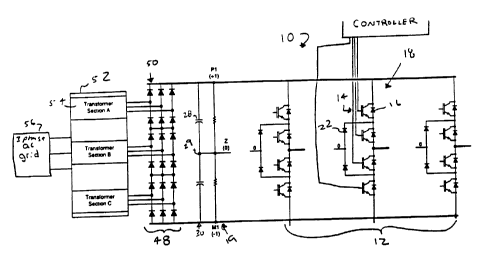
FIG.1 is a cirouit diagram of a non-regenerative converter 10 with low grid
current distortion and active neutral charge balance control, and FIG. 2 is a
circuit
diagram of a regenerative converter 11. Both embodiments include a three level
output power conversion stage 12. The output power stage includes electrical
3 0 switches 14 which are shown as IGBTs (Insulated Gate Bipolar Transistors).
Other
useful switches include GTOs (Gate Tum Off Thyristors) and IGCTs (Integrated
Gate
Commutated Thyristors). The switches are paired with anti-parallel
freewheeling
diodes 16 to accommodate the inductive motor load currents. A controller 15,
shown
in FIG. 1, is used for controlling each of the switches. The controller
comprises a
3 5 computer and in a preferred embodiment includes a digital signal
processor.
CA 02249871 1998-10-08
RD 25735
-4-
FIG. 3 is a circuit diagram of an individual NPC three level phase leg 18 of
FIG. 1 and FIG. 2. The three phase inverter has four switch and diode pairs
spanning
the DC bus (with a positive rail labeled P-Bus 20, a negative rail labeled N-
Bus 24,
and a midpoint of the bus labeled midpoint 26) and two clamping diodes 22
(labeled
D5, D6). The switch diode pairs are labeled top to bottom S1/D1, S2/D2, S3/D3,
S4/D4. As shown in Table 1, there are three command states for the switches
per
phase.
STATE 1 S1 ON S2 S3 OFF S4 LOAD PT ~ P-BUS
(+) ON OFF
STATE 2 S1 OFF S2 S3 ON S4 LOAD PT ~ MID-POINT
(O) ON OFF
STATE 3 S1 OFF S2 S3 ON S4 LOAD PT ~ N-BUS
(-) OFF ON
Tabl e 1 tates
NPC
S
Depending on the switch commanded state per phase, and the instantaneous
polarity of the load current in that phase, the load current path can be
through
switches, freewheeling diodes, or clamping diodes. For example, if the
commanded
state is STATE 2, and the load current is positive, the load current path is
through
clamp diode D5 and switch S2. If the commanded state is STATE 2, and the load
current is negative, the load current path is through switch S3, 'and clamp
diode D6.
Table 1 shows the load terminal per phase can be either at P-bus, N-bus, or
DC bus midpoint, which gives rise to the terminology three level or neutral
point
clamped inverter. In a two level inverter, the load terminal per phase is
either at P-bus
2 0 or N-bus. This extra load point level, that is, the DC midpoint, in the
three level
inverter accounts for its lower load current harmonic amplitudes than a two
level
inverter chopping at the same frequency.
The second advantage of the three level inverter is that with four switches
spanning the DC bus, each with a maximum working DC voltage equal to one half
the
2 5 DC link voltage, twice the output voltage for a given switch voltage
rating can be
obtained compared to a two level inverter. This is achieved without the need
to gate
the switches directly in series and thus tum-on, tum-off voltage sharing
complications
are avoided.
The capacitor 28 bank 30 midpoint (at DC midpoint 26) and the clamping
3 0 diodes 22 connected between capacitor bank midpoint and switches S1/S2 and
S3/S4 respectively keep the maximum DC working voltage across any switch from
exceeding one half of the DC bus voltage (Vdc/2), provided the DC filter
capacitor
midpoint voltage is maintained at Vdc/2. Regulators are built into the
modulator to
keep the midpoint voltage at Vdc/2 to guard against long term unequal
discharge of
3 5 the two capacitor bank halves. The resistor network 19 (shown in FIGs. 1
and 2)
CA 02249871 1998-10-08
RD 25735
-5-
across the DC bus capacitor bank serves as a fixed safety bleed resistor and a
balance network for initial capacitor charging.
FIG. 4 is a circuit diagram of optional snubber circuits 32 applied to inner
switches 14a of the NPC phase leg of FIG. 3. A snubber diode 34 will tum on
during
switch tum-off whenever the voltage across the device exceeds the positive
portion
20 of the bus, effectively placing the snubber capacitor 36 in parallel with
switch 14a.
The capacitor will transiently absorb the excess energy stored in the
parasitic circuit
inductances in series with the switch. After the switch is turned off, the
ringup voltage
across the snubber capacitor is dissipated in the snubber resistor 38. The
snubber
elements are sized to keep the switching trajectory of voltage and current
within the a
safe operating area. If IGBT switches are used, an inverter will typically be
constructed with low inductance circuit paths and buswork so that at low
current levels
the phase leg can be safely,switched. The inner switches 14a (S2 8~ S3)
commutate
current between higher inductance circuit paths as compared to outer switches
14b
(S1 8 S4) with current switching through four device elements rather than two
device
elements. Consequently, the inner switches will experience greater voltage
overrings
and can require snubbers.
FIG. 5 is a circuit diagram of optional snubber circuits applied to outer
switches of the NPC phase leg of FIG. 4. The illustrated outer switch snubbers
also
2 0 act to clamp the overring across the switch to half the DC bus during
device turnoff.
Snubber diode 42, snubber capacitor 44, and snubber resistor 46 of FIG. 5
operate
on the outer switches in the same manner as snubber diode 34, snubber
capacitor
36, and snubber resistor 38 of FIG. 4 operate on the inner switches.
Low harmonic distortion of grid current is important for the IEEE-519 standard
2 5 which requires a measurable objective of less than five percent total
demand
distortion at the grid connection. Either a non-regenerative or a regenerative
circuit
can be used, based on the specific drive application, to meet this standard.
The non-regenerative variant of this invention illustrated in FIG. 1 includes
an
eighteen pulse diode rect'rfier 48 to convert the AC grid 56 power into the DC
bus
3 0 power required for the NPC voltage source inverter. Low grid current
distortion is
important to avoid excessive harmonic distortion on the utility grid. The
eighteen pulse
series connection of three six pulse diode rectifier bridges 50 is most useful
with a
grid transformer 52 with three isolated sets of three phase transformer
secondaries
54 with 20 degree phase separation between the three sets. Although eighteen
pulse
3 5 diode rectifiers are preferred, other diode rectifiers can alternatively
be used.
One alternative embodiment (not shown), for example, capable of achieving
the requisite IEEE-519 current distortion levels is a twenty four pulse
configuration
including four six pulse rectifiers in series fed from a grid transformer with
secondary
CA 02249871 1998-10-08
RD 25735
-s-
sets of 15 degree phase separation. This circuit has an advantage in that the
split DC
bus required for the NPC output converter stage can be achieved by feeding two
series rectifier bridges into the upper half of the capacitor bank and the
remaining two
rectifier bridges into the lower half of the capacitor bank. This stiff
independent power
feed obviates the need for active control of neutral voltage balance. This
option
however increases number of diode components, increases the transformer
complexity, and increases cabling costs.
Another aftemative embodiment (not shown) is a twelve pulse configuration
including two six pulse rectifier bridges. This embodiment includes less diode
components and complexity at the expense of additional distortion.
The IEEE 519-1992 harmonic limits are a function of the ratio of line short
circuit, Isc, to drive rated current, III. For ratios below twenty, the
harmonic current
limits expressed in terms of Total Demand Distortion (TDD) are given in Table
2. This
measure differs from total harmonic distortion since harmonic content is
measured
relative to drive rated current. Overall current TDD must be less than five
percent.
Harmonic (h) Range TDD Limit
1 <h<13 49' h odd - 1 % h even
11 <h<19 . 2% h odd - 0.5% h even
17<h<25 1.5% h odd - 0.375~ h even
23<h<35 0.6% h odd - 0.15% h even
Total Demand Distortion, {[Sum(I,,'-I,')j''/I,}'100%
all < 5%
harmonics
Table 2 IEEE-519-1992 Harmonic Current Limit Requirements
2 0 In addfion, due to special harmonic generation properties of eighteen
pulse rectifiers,
the TDD limits for eighteen pulse rect'rfiers for its characteristic harmonics
can be
increased by a factor of 1.73 provided the amplitudes of the non-
characteristic
harmonics are twenty five percent of the limits specified in the tables. IEEE
519-1992
also restricts the line voltage distortion. The total harmonic distortion
(THD) with a
2 5 maximum line impedance of five percent should not exceed five percent with
each
individual harmonic not exceeding three percent THD.
FIG. 6 is a circuit diagram of an optional dynamic braking (DB) circuft 58 for
a
non-regenerative converter. A DB resistor 60 is supplied to transiently
dissipate
energy stored in the rotating inertia which is regenerated into the DC bus
during motor
3 0 deceleration. DB switches 62 are gated in synchronism based on measured DC
bus
voltage (whenever the DC bus voltage rises to above the high line level). The
CA 02249871 1998-10-08
RD 25735
_7_
controller should provide adequate hysteresis in order to both limit maximum
bus
voltage, DB switching frequency, and device switching losses. A freewheeling
diode
path 64 is supplied to accommodate inductive current paths to the DB resistor.
A
diode clamp path 65 to the DC bus neutral is supplied to allow for timing
variances in
the two DB switches.
FIG. 2 illustrates a full regenerative embodiment which will typically be used
in
high performance motor 74 drives or drives which must quickly decelerate high
inertia
loads. The power conversion stage 66 includes an NPC converter bridge similar
to
the NPC converter bridge 12. The embodiment of FIG. 2 is capable of arbitrary
load
power factors while providing a unity power factor interface to the grid.
The input 'rectifier' bridge 66 with three phase legs 68 serves as a PWM
boost converter n3gulating the overall DC bus voltage. The input converter 66
interfaces to the utility grid 56 through an input stage filter assembly 70
which will fitter
the high frequency switching harmonics from the three phase converter current.
An
input stage transformer can be an integral part of the inductive elements in
the grid
filter. The DSP controller will regulate the three phase input current flow.
The power circuit should be supported by active DC neutral voltage balance
control, and, in the present invention, the active control is supplied by a
predictive
charge calculation method. If the DC neutrals of the two converters are
connected,
2 0 then the charge balance of the combined split capacitor bank can be
maintained by
either of the two converters. The load side is generally to be preferred to
free the
souroe converter control for grid current regulation. Altemat'rvely, the
source and load
converters can maintain separate neutrals with no common connection. In this
case
both modulation controls must independently maintain neutral charge balance.
2 5 FIG. 7 is a circuit diagram of a ground reference network which is
preferably
coupled between the DC neutral point 26 and a ground frame 73. The ground
reference network impedance is chosen to approximately match motor cable
characteristic impedance. The voltage across the ground reference network is
monitored by the controller for ground fault detection.
3 0 Preferably, a digital signal processor (DSP) based drive controller uses
active
neutral control by gate timing manipulation in order to maintain equal voltage
balance
on the split series capacitor bank (between the upper and lower halves of the
DC
link). It is desirable to also have tight control of the neutral charging
currents in order
to minimize the capacitance values required.
3 5 In one embodiment, the controller is an entirely software based system
executed in a computer with interface circuits for voltage and current
feedback data
acquisition and digital timers for switch activations based on DSP computed
timings.
The DSP will include vector control of both machine torque and flux. The DSP
will
CA 02249871 1998-10-08
RD 25735
.g_
also include a space vector modulation control for the NPC converter bridge.
Additionally, the DSP will include active DC bus neutral voltage control by
gate timing
manipulation in order to maintain equal voltage balance on the split series
capacitor
bank.
A modulator control algorithm of the present invention executes in the DSP
controller by requiring only three additional hardware timers, one per phase,
for
actuation. The control algorithm is an extension of the space vector synthesis
approach developed for two level inverters. wick response to an arbitrary
reference
voltage vector is ensured by an immediate warp transition between home
vertices
followed by adjacent vector modulation. Neutral voltage control is achieved by
choosing amongst alternative vectors based on measured voltage error and
predicted
charge using either measured or reference phase currents. The predicted charge
method ensures maximum neutral corrective effort regardless of load power
factor.
FIG. 8 is a diagram of three level pulse width modulated (PWM3) space
vectors illustrating the complex voltage plane defined by the orthogonal a, ~
voltage
axes and indicating the direction of phase voltages A, B, C. The a and A phase
axes
align with the peak of the phase A voltage wave. The hexagonal outer boundary
indicates the reachable voltages defined by the magnitude of the DC bus
voltage
(Vdc). The vertices of the individual triangular regions are denoted by a
three digit
2 0 gating state, one digit per phase, in ABC order. Each digit can assume a -
, 0, or +
value representing the three voltage levels available in an inverter phase
leg. The
reference voltage vector V' is denoted rotating at frequency w, in a counter
clockwise
direction. For smooth voltage synthesis during steady state conditions the
reference
voltage vector will sweep through adjoining triangular regions at a sinusoidal
2 5 frequency and a substantially constant magnitude. Space vector synthesis
will create
the desired voltage by time modulating between the three comer vertices of the
triangular region containing the reference voltage vector tip.
FIG. 9 is a diagram of sector/triangle indices and home vertices illustrating
the modulator control segmenting the complex voltage plane. Twelve sectors, 30
3 0 degrees in arc, are defined (ds = 0-11 ). Each 30 degree sector is further
subdivided
by magnitude into three triangular zones (ms=0-2). The reference voltage
vector is
assigned a ds index according to the reference angle to the a axis and an ms
index
based on reference amplitude. The combination of ds and ms indices defines one
of
36 triangular zones within the reachable voltage hexagon. Once the correct
triangular
3 5 zone has been located, a home vertex position is defined per FIG. 9 as a
vertex in
common with one of the triangle comers and in a position closest to the center
of the
diagram. There are 7 home vertices: one (+++/000/---) for all the twelve inner
triangular zones (ms = 0 8~ ds = 0-11 ) and six (+00/0--, ++0100-, 0+0/-0-,
0++/-00,
CA 02249871 1998-10-08
RD 25735
_g_
00+/--0, +0+/0-0) for the 24 outer triangular zones (ms = 1 or 2). For
example, if a
reference voltage vector were in a triangular zone X1-X4, the home vertex
would be
v6. Each modulation vector sequence always begins and ends on a home vertex.
The redundant choices in voltage vertices enables simultaneous voltage
synthesis
and charge balance as explained below.
FIG.10 is a set of graphs illustrating PWM3 inner triangle modulation. The
reference voltage vector sequence begins at the home vertex 000. For each
gating
frame (or period), the switching pattern proceeds to the comer vertices
defining the
triangular region, switching one phase at a time (000 to +00 to ++0 to +++)
with one
transition defined per phase, ending at the home vertex +++. The DSP computes
the
relative dwell times at each comer vertex in order to achieve the desired
reference
voltage vector, on the average, over the gating frame. The following
calculation
solves a set of simultaneous linear equations to compute the dwell times t03,
t1, and
t2 with the zero vector dwell time (t03) further subd'rvded equally into t0
(000 dwell
time) and t3 (+++ dwell time):
.
m= 2.'V ~, mcosd =m~cos(b~, msind=m~sin(b~,
mcosd 2 2'cos 3 0 kl
msind = 0 1 sin ~ 0 k2
1 1 2 1 3 1 k03
tl=kl~dtpwm, t2=k2~dtpwm, t03=k03~d<pwrr~,
wherein d is the angle from the reference voltage vector to the closest axis,
dtpwm is
the gating interval time, V' is the reference voltage vector, V~ is the
measured
voltage, S is an angle of the reference voltage vector with respect to a side
of the
triangular zone in which the reference voltage vector is present, k03 is the
per unit
2 5 dwell time at the home vertex, k1 is the per unit dwell time at the first
comer vertex,
and k2 is the per unit dwell time at the second corner vertex. The DSP outputs
gating
times and gating states for each phase; e.g. for this sequence t0 for A, t0+t1
for B,
t0+t1+t2 for C. The timers are synchronously activated every gating period.
After each gating frame, at the next sampling instant, in a preferred
3 0 embodiment the appropriate next switching pattern is determined. If the
reference
voltage vector is in the same triangular zone as in the previous gating frame,
a
second gating frame traverses the vertices in the opposite sequence (+++ to
++0 to
CA 02249871 1998-10-08
RD 25735
-10-
+00 to 000) from the first gating frame. The described switching pattern uses
only the
0 and + gating states for each phase. This has the effect of discharging the
upper
half capacitor bank when motoring. The first and second gating frames form a
gating
frame pair.
To continue to maintain charge balance on the capacitor halves, if the
reference voltage vector remains in the same triangular zone the sequence of
first
and second gating frames can alternate with a minus gating state sequence as
in the
second pair of gating frames illustrated by FIG. 10 (000 to 00- to 0- to ---
followed by
-- to 0-- to 00- to 000).
Depending on the modulation algorithm, after the completion of (1 ) each
gating frame, (2) each pair of gating frames, or (3) two pairs of gating
frames, at the
sampling instant prior to the beginning of the next gating frame, whether or
not the
reference voltage vector remains in the same triangular zone, altemat'rve
gating
sequences are possible: a positive sequence 000 to +++, a negative sequence
000 to
---, or, for option (1) where the test is performed after each gating frame,
one of the
opposite sequences discussed above (+++ to 000 or --- to 000).
To actively control neutral charge balance for inner triangle modulation, the
net charge injected into the DC bus neutral is computed for available
alternatives as
the sum of the product of the phase current (i,~ and the neutral dwell time
(dt",~ for
2 0 each phase q=F,k.,_.~ (ik*bt",~. The altemat'rve is chosen, based on the
polarity of the
predicted neutral charge, to correct for any measured neutral voltage error.
If the
neutral voltage error is small (i.e. within a small deadband) positive and
negative
gating sequences will alternate. If the reference voltage vector changes
triangles,
then the home vertex will switch to be the home vertex of the new triangular
zone in
2 5 which the reference voltage vector is situated.
FIG. 11 is a set of graphs illustrating PWM3 outer triangle modulation, i.e.,
when the reference voltage vector magnitude is greater than 3~ maximum. The
modulation sequence starts at the home vertex (gstate=+00) and proceeds
switching
one phase at a time from +00 to +0- to +-- returning to the home vertex
(gstate=0--).
3 0 The dwell times at each triangle vertex (t03, t1, and t2) are again
computed by solving
a set of simultaneous linear equations for ms=1:
~ 1 ~r 1
cos- ~ - ~ _
cos- cos-
necosd6 6 2 3 2 kl
msind = cos 1 ~ 0 k2
~ ~ sin sin
~ ~
6 2
6 3
1 1 1 1 k03
or for ms=2:
CA 02249871 1998-10-08
RD 25735
_»_
1 cos ~ . cos ~ 1
mcosd 6 6 2 kl
msind = 0 cos 6 .sin 6 0 k2
1 1 1 1 k03
If no neutral correction is required, the home vertex dwell time is subdivided
equally
into t0 (+00 dwell time) and t3 (0--dwell time). The second half gating frame
reverses
the gating sequence 0-- to +-- to +0- to +00. Actual gating actuation is again
controlled
by per-phase synchronously activated timers.
Neutral voltage control for outer triangle modulation is achieved by adjusting
relative dwell times for the redundant gating states of the home vertex (t0
vs. t3 time)
while keeping their sum fixed. The relative charge injection for the two
aftemat'rves is
again computed as the sum of the product of phase current (i,~ and neutral
dwell
time (dt",~ for each phase. The two aftemat'rves will have equal and opposite
effect.
Either t0 or t3 will be maximized, based on the polarity of the predicted
neutral charge,
to correct for any measured neutral voltage error. The dwell times are
assigned to
maximize the corrective action i.e. assigning t = t03 - tminz to the selected
alternative
and tminz to the other, where tminz is a minimum pulse width time. The maximum
corrective action Corresponds to a bang-bang control strategy. A linear
controller w'tth
proportional correction can also be implemented. Optionally, ff the neutral
voltage
error is small (i.e. within a small deadband) the t0 and t3 times can be set
equally
without applying a corrective effort.
FIG. 12 is a diagram of PWM3 space vector transient illustrating the warp
2 0 transition mode which facilitates rapid transient response for vector
controlled drives.
Two successive reference voltage vectors are shown Vk' and Vk,,'. The
algorithm will
force a synchronous transition from the old home vertex (time t,~ to the new
home
vertex (time tk,~). Each home vertex gating state is assigned a polarity
weight index
ranging between -3 through +3 (e.g. gstafe=+00 has a weight of +1 ). The warp
2 5 transition chooses the gating state of the new home vertex to minimize the
change in
the polarity weight index. After transitioning to the new home vertex, a
conventional
outer triangle modulation sequence is computed for the next half gating frame.
In this
manner there is no delay introduced in synthesizing the next reference voltage
vector.
The same algorithm is also applied to transitions within the inner triangles
and
3 0 between inner and outer triangles.
Overmodulation (non-linear production of high output voltages) is possible
with this control system. Overmodulation can be achieved by pulse dropping
and/or
shifting the reference voltage vector angle towards the closest axis, thereby
reaching
CA 02249871 1998-10-08
RD 25735
_ ~2 _
the reference voltage vector magnitude while still respecting the minimum
pulse width
constraint.
While only certain preferred features of the invention have been illustrated
and described herein, many modifications and changes will occur to those
skilled in
the art. It is, therefore, to be understood that the appended claims are
intended to
cover all such modfications and changes as fall within the true spirit of the
invention.