Note: Descriptions are shown in the official language in which they were submitted.
CA 02249938 2001-07-03
MULTIPLE INVERTER SYSTEM
FIELD OF THE INVENTION
The present invention relates to an inverter system
to obtain several kV high voltage outputs and more
particularly to a multiple inverter system designed to
obtain high voltage output using a plurality of unit
inverters.
BRIEF DESCRIPTION
OF THE DRAWINGS
A more complete appreciation of the present invention
and many of the attendant advantages thereof will be
readily obtained
as the same
becomes
better understand
by
reference to the following detailed description when
considered in connection with the accompanying drawings,
wherein:
FIG.1 is a circuit diagram for explaining a first
example of a conventional multiple inverter system;
FIG.2 is a circuit diagram for explaining a second
example of a conventional multiple inverter system;
FIG.3 is a circuit diagram for explaining a third
example of a conventional multiple inverter system;
FIG.4 is a circuit diagram showing essential
portions
only for
explaining
a conventional
multiple
inverter
system;
FIG.5 is a circuit diagram for explaining a first
embodiment of a multiple inverter system of the present
invention;
FIG.6 is a circuit diagram for explaining a second
embodiment of the multiple inverter system of the present
invention;
FIG.7 is a circuit diagram of an inverter for
explaining a second embodiment of a multiple inverter of
1
CA 02249938 2001-07-03
the present invention;
FIG.8 is a circuit diagram for explaining a third
embodiment of a multiple inverter system of the present
invention;
FIG.9. is a circuit diagram for explaining a fourth
embodiment of a multiple inverter system of the present
invention;
FIG.10 is a circuit diagram for explaining a fifth
embodiment of a multiple inverter of the present
invention;
FIG.11 is a circuit for explaining a sixth
embodiment of a multiple inverter system of the present
invention;
FIG.12 is a circuit diagram for explaining seventh
a
embodiment of a multiple inverter system of the present
invention;
FIG.13 is a signal waveform diagram for explaining
an eighth mbodiment of a multiple inverter system of
e the
present inv ention;
FIG.14 is a circuit diagram for explaining a ninth
embodiment of a multiple inverter system of the present
invention;
FIG.15 is a circuit diagram of an inverter
for
explaining a tenth embodiment of a multiple inverter
system of he present invention;
t
FIG.16 is a circuit diagram of an inverter
for
explaining an eleventh embodiment of a multiple inverter
system of he present invention;
t
FIG.17 is a circuit diagram of an inverter
for
explaining a twelfth embodiment of a multiple inverter
system of the present invention;
FIG.18 is a circuit diagram of an inverter for
explaining a thirteenth embodiment of a multiple inverter
2
CA 02249938 2001-07-03
system of the present invention;
FIG.19 is a circuit diagram of an inverter for
explaining a fourteenth embodiment of a multiple inverter
system of the present invention;
FIG.20 is a signal waveform diagram for explaining a
fourteenth embodiment of a mufti-inverter system of the
present invention;
FIG.21 is a circuit diagram of an inverter for
explaining a fifteenth embodiment of a multiple inverter
system of the present invention;
FIG.22 is a signal waveform diagram for explaining a
sixteenth embodiment of a multiple inverter system of the
present invention;
FIG.23 is a diagram for explaining a seventeenth
embodiment of a multiple inverter system of the present
invention;
FIG.24 is a circuit diagram for explaining an
eighteenth embodiment of a multiple inverter system of
the present invention;
FIG.25 is a circuit diagram for explaining a
nineteenth embodiment of a multiple inverter system of
the present invention;
FIG.26 is a circuit diagram for explaining a
twentieth embodiment of a multiple inverter system of the
present invention;
FIG.27 is circuit diagram for explaining a twenty-
first embodiment of a multiple inverter system of the
present invention;
FIG.28 is a signal waveform diagram for explaining a
twenty-second embodiment of a multiple inverter system of
the present invention;
FIG.29 is a circuit diagram for explaining a twenty-
third embodiment of a multiple inverter system of the
3
CA 02249938 2001-07-03
present invention;
FIG.30 is a diagram for explaining a twenty-fourth
embodiment of a multiple inverter system of the present
invention;
FIG.31 is a schematic diagram
of the transformer for
explaining a twenty-fifth embodiment of a multiple
inverter system of the present
invention;
FIG.32 is a circuit diagram
showing a main circuit
of a multiple type inverter
to which the present
invention is applied;
FIG.33 is a circuit diagram showing essential
portions only for explaining a thirtieth embodiment of
a
multiple inverter system of he present invention;
t
FIG.34 is a diagram for explaining one example of
a
unit inverter control means hown in FIG.33;
s
FIG.35 is a circuit diagram showing essential
portions only for explaining a thirty-first embodiment
of
a multiple inverter system of the present invention;
FIG.36 is a circuit diagram showing essential
portion only for explaining thirty-second embodiment
a of
a multiple inverter system of the present invention;
FIG.37 is a circuit diagram showing essential
portions only for explaining a thirty-third embodiment
of
a multiple inverter system of the present invention;
FIG.38 is a circuit diagram showing essential
portions for explaining a thirty-fourth embodiment of a
multiple inverter system of the present invention;
FIG.39 is a circuit diagram showing essential
portions only for explaining a thirty-fifth embodiment of
a multiple inverter system of the present invention;
FIG.40 is a circuit diagram showing essential
portions only for explaining a thirty-sixth embodiment of
a multiple inverter system of the present invention;
4
CA 02249938 2001-07-03
FIG.41 is a circuit diagram showing essential
portions only for explaining a thirty-seventh embodiment
of a multiple inverter system of the present invention;
FIG.42 is a circuit diagram showing essential
portions only for explaining a thirty-eighth embodiment
of a multiple inverter system of the present invention;
and
FIG. 43 is a diagram for explaining deformed examples
of the embodiments of a multiple inverter system of the
present invention.
DESCRIPTION OF THE RELATED ART
So far, there are many needs for energy saving by
variable speed drive operation of AC motors,
particularly, existing high-voltage motors. In
particular, a high-voltage driving system is demanded,
which is applicable directly to existing high-voltage
motors; e.g., 3k system, 6kV system in Japan and 4.2 kV
system and 2.4 kV system in overseas.
A general method so far used to construct a power
conversion system for obtaining high voltage is a method
to connect secondary windings of a plurality of
transformer in series as described in Section 3 of the
technical report titled "Multiple-Power Converter and
Application Technology thereof" published from The
Institute of Electrical Engineers of Japan (July, 1995).
An example of a high-voltage 12-phase inverter system
that is so far often used is shown in FIG. 1.
This inverter system is composed of a rectifier 110,
which converts AC to DC, a DC smoothing circuit 120
comprising a reactor 121 and a capacitor 122, inverter
circuits 130 and 131, which convert DC to AC of optional
frequency, transformers 140 and 141 and a load 150.
5
CA 02249938 2001-07-03
This circuit is in a structure that DC output of the
rectifier 110 is commonly used, a plurality of inverter
circuits 130, 131 are provided for this DC voltage and
the secondary side windings of the output transformers
140, 141 are connected in series so as to obtain a
desired high voltage.
A control circuit is composed of a speed command unit
162, a transmitter (OSC) 163, which decides the output
frequency in the inverter circuits 130, 131, a
distributor (RING) 164, which distributes the signal from
the transmitter 163 to semiconductor devices in the
inverter circuits 130, 131, an amplifier 165, a voltage
control circuit (AVR) 166, a phase shifter (PHC), which
decides a gate signal phase of the rectifier 110, a
voltage detecting transformer 143, which detects the
output AC voltage of the output transformers 140, 141 and
the voltage detected by the voltage detecting transformer
143 is input to one of the input terminals of a
comparator 134 via a reverse current preventing diode
144, a command from the speed commanding unit 162 is
input to the other input terminal of the comparator 145
and a deviation obtained by the comparator 145 is given
to a voltage control circuit 166.
A circuit shown in FIG.2 is in a structure to obtain
a high-voltage by combining a plurality of mutually
insulated inverter circuits 130, 131 by the output
transformers 140, 141, and excepting these elements,
other component elements which are the same as those
shown in FIG.l are assigned with the same reference
numerals used in FIG.1 and their explanations are
omitted.
This circuit is in such a structure that an inverter
circuit is provided to each of the outputs from the
6
CA 02249938 2001-07-03
rectifiers 110, 111 and the secondary windings of the
output transformers are connected in series so as to
obtain a desired high-voltage.
In the case of the structure shown in FIG.l and
FIG.2, the output transformers 140, 141 are required for
the outputs of the inverter circuits 130, 131,
respectively and therefore, an area needed for installing
them becomes large. Furthermore, to make the output
transformers 140, 141 to be durable for the use from low
frequency, there is such a defect that their external
shape becomes larger than ordinary transformers of fixed
frequency.
Further, a neutral point clamped 3 level inverter
shown in FIG.3 has been developed and put in practical
use in recent years. This inverter converts the AC output
from an AC power source 11 into DC by a rectifier 12 and
after smoothed by capacitors 13, 14, supplies AC output
obtained from a 3 level inverter circuit using 3 sets of
a circuit comprising self-turn-off semiconductor devices
Sl~S4 composed of, for instance, a gate turn-off
thyristor (GTO) and diodes Dl~D6 to a load motor 16.
Further, P, N indicate control buses and C indicates a
neutral-point potential.
A multiple level inverter as shown in FIG.3 has an
economical problem that the connection of semiconductor
devices in series becomes necessary because the circuit
voltage becomes equivalent to the output voltage and a
size of the system becomes large because the dielectric
strength becomes high.
For a conventional system in the structure as
described above, there exist such problems as shown
below. As technical problems when comprising a high-
vol_tage converter, the following matters are pointed out.
7
CA 02249938 2001-07-03
(1) If an inverter circuit is constructed without
connecting semiconductor devices in series, an output
transformer are required, which is not economical.
(2) If an inverter circuit is constructed by
connecting semiconductor devices in series, an output
transformer can be eliminated but the system may not
become fully reliable because it becomes necessary to
select semiconductor devices that are to be connected in
series and the gate control becomes complicated.
(3) In the serially connected structure of
semiconductor devices, the harmonic reduction is limited
as a matter of course because the output side harmonic
component is decided by PWM switching frequency of
semiconductor devices.
(4) If even one of a lot of semiconductor devices
comprising the main circuit becomes defective, the
continuous operation of the system becomes impossible and
it becomes a problem in a system demanded for the
continuous operation.
Further, in particular, when the high-voltage output
obtained by connecting the output sides of a plurality of
unit inverters in series is supplied to an AC load, there
are problems as shown below.
FIG.4 shows an example of a definite circuit using
this type of conventional multiple inverter system. The
structure shown in FIG. 4 will be described below. That
is, this circuit is provided with a rectifier 2, which
converts AC voltage of an AC power source Al into DC
voltage, a unit inverter, which converts DC power of the
rectifier A2 into AC power, connected to the rectifier A2
in parallel with it via a smoothing capacitor A3,
provided with four bridge connected semiconductor devices
A5, A6, A'7, A8 of, for instance, IGBT and the like and a
8
CA 02249938 2001-07-03
gate controller A40 to give a firing command in the
specified order to the semiconductor devices A5~A8
comprising the unit inverter A9.
Although not shown in FIG.4, a plurality of the unit
inverters 9 including the same smoothing capacitor A3 as
the structure described above are provided, the input
sides of the unit inverters A9 are connected to the
rectifier A2 in parallel with it and the output sides of
the unit inverters A9 are connected in series, and an AC
load A10 that is, for instance, an induction motor is
connected to the output side of the thus connected
multiple inverter.
The unit inverter A9 is provided with a bypass
circuit described below to protect the unit inverter A9.
The bypass circuit is connected between the buses of the
input side of the AC load A10 and is composed of a bypass
switch A41 comprising, for instance, a thyristor, a diode
bridge comprising diodes A42, A43, A44, A45 connected
between the bypass switch A41 and the AC load A10, a
current detector A46 to detect load current and a switch
operating circuit A47 which gives an ON command to the
bypass switch A41 when the current value detected by the
current detector A46 exceeds a specified value.
The bypass circuit is also incorporated in other unit
inverters (not shown) than the unit inverter A9.
In FIG.4, when the unit inverter A9 is in the normal
state without causing a short-circuit, etc., the bypass
switch A41 is kept in the OFF state and it therefore
performs nothing.
However, when the semiconductor devices A5, A8 of one
of a plurality of unit inverters A9 are not short-
circuited completely but short-circuited except, for
instance, the IGBT bonding wire, the current value
9
CA 02249938 2001-07-03
detected by the current detector A46 exceeds a specified
value and therefore, the switch operating circuit A47
operates and the bypass switch A41 is turned ON. As a
result, the short-circuit current flowing to the load A10
flows in the direction of arrow.
The operation described above is in the case of an
ideal circuit where there is no delay in the operation
for the period when the current detector A46 detects an
abnormality of the unit inverters A9 and turns the bypass
switch A41 ON. Therefore, the short-circuit current flows
to the AC load A10 as a result of the short-circuit of
the unit inverter A9, unless the operation of the short-
circuited unit inverter A9 is once stopped, the AC load
A10 can be burnt out.
SUMMARY OF THE INVENTION
The present invention has been made to improve such
problems as described above and an aspect of one of the
objects of the present invention is to provide an
economical multiple inverter system, which requires no
output transformer, is small in size but capable of
obtaining a high-voltage output, reducing higher harmonic
to a load side and also, reducing harmonic current of the
input power source.
Further, an aspect of another object of the present
invention is to provide a multiple inverter system
capable of continuously operating an AC load even when a
short-circuit and other troubles are taken place on at
least one of unit inverters without suspending the
operation of the remaining good unit inverters.
In order to achieve the aspects of the above-
mentioned objects, in a multiple inverter system of the
present invention, comprising each phase by connecting a
CA 02249938 2001-07-03
plurality of input transformers having secondary windings
and unit inverter cells in series for n stages and
supplying electric power to multiple phase loads in
combination with the input transformers, the input
transformer has 3n sets of three-phase windings at the
secondary side and the secondary windings of the
transformers which are out-of-phase at each phase are
connected to unit inverter cells of all phases at the n-
th stage.
Further, in order to achieve the aspects of the
above-mentioned objects, a multiple inverter system of
the present invention is provided with input transformers
having 3n sets of three-phase secondary windings, at
least one three-phase inverter and a plurality of single-
phase inverter cells, which are serially connected for a
plurality of stages (n-1) to form multiple phases and are
connected to the same phase of the three-phase inverter
and supply the electric power to a multiple phase load.
According to the present invention, when
transformers having multiple secondary windings are
combined with unit inverter cells, it is possible to
obtain an economical multiple inverter system, which
requires no output transformers and is capable of
obtaining high voltage output from a small sized system,
and reducing higher harmonic to a load side as well as
harmonic current of a power source system.
Further, in order to achieve the aspects of the
above-mentioned objects, a multiple inverter system of
the present invention is in a structure that n units of
input transformers are provided for n unit of serially
connected unit inverter cells for each phase, each of the
transformers has 3 sets of three-phase windings which are
7z/3n shifted in phase each other at the secondary side
11
CA 02249938 2001-07-03
and the secondary windings which are out-of-phase at each
phase are connected to the unit inverter cells at the n-
th stage of each phase.
Further, in order to achieve the aspects of the
above-mentioned objects, a multiple inverter system of
the present invention comprises: rectifiers which convert
AC power into DC power, a plurality of voltage source
unit inverters which convert DC power of rectifiers into
AC power and are connected with a plurality of bridge
connected semiconductor devices, a group of unit
inverters of which input sides are connected in parallel
to the rectifiers via smoothing capacitors respectively
and the output sides are connected in series and to AC
load, fuses serially connected between the rectifiers
and the unit inverters, bypass switches connected to the
unit inverters in parallel with them and form a circuit
to circulate load current when it is electrically closed,
a pulse width modulation unit inverter control means to
give a firing command in the specified order to
semiconductor devices comprising the unit inverters, an
abnormality judging means to judge a fault relative to
the unit inverter control means and when the abnormality
judging means judges the abnormality, and a bypass
control means to melt a fuse by giving a circuit closing
command to the bypass switch of the applicable unit
inverter when the abnormality judging means judges the
abnormality.
Further, in order to achieve the aspects of the
above-mentioned objects, a multiple inverter system of
the present invention comprises: rectifiers which convert
AC power into DC power, a plurality of voltage source
unit inverters which convert DC power of rectifiers into
AC power, comprising a plurality of bridge connected
12
CA 02249938 2001-07-03
semiconductor devices, a group of unit inverters of which
input sides are connected in parallel to the rectifiers
via smoothing capacitors and the output sides are
connected in series and further to an AC load, fuses
serially connected between the rectifiers and the unit
inverters, bypass switches connected to the unit
inverters in parallel with them and form a circuit to
circulate load current when it is electrically closed, a
pulse width modulation unit inverter control means to
give a firing command in the specified order to
semiconductor devices comprising the unit inverters, an
abnormal operation detecting means to detect the abnormal
operating state of the unit inverter based on the AC
output of the unit inverter, a DC abnormality detecting
means to detect the abnormality of DC input of the unit
inverter and a bypass switch control means to melt the
fuse by giving a circuit closing command to the bypass
switch corresponding to applicable unit inverter, and
operates by increasing a modulation factor of the unit
inverter in the phase causing the abnormality out of the
group of inverters to more than one time by the unit
inverter control means.
Further, in order to achieve the aspects of the
above-mentioned objects, a multiple inverter system of
the present invention comprises: rectifiers which convert
AC power into DC power, a plurality of voltage source
unit inverters which convert DC power of rectifiers into
AC power, comprising a plurality of bridge connected
semiconductor devices, a group of unit inverters of which
input sides are connected in parallel with the rectifiers
via smoothing capacitors and the output sides are
connected in series and further to an AC load, fuses
serially connected between the rectifiers and the unit
13
CA 02249938 2001-07-03
inverters, bypass switches connected to the unit
inverters in parallel with them and form a circuit to
circulate load current when it is electrically closed, a
pulse width modulation unit inverter control means to
give a firing command in the specified order to
semiconductor devices comprising the unit inverters, an
abnormal operation detecting means to detect the abnormal
operating state of the unit inverter based on the AC
output of the unit inverter, a DC abnormality detecting
means to detect the abnormality of DC input of the unit
inverter and a bypass switch control means to melt the
fuse by giving a circuit closing command to the bypass
switch corresponding to applicable unit inverter, and
operates the number of inverters in the healthy phase
corresponding to the number of inverters in the phase
detected by the abnormal operation detecting means.
In accordance with another aspect of the present
invention, there is provided a multiple inverter system,
comprising:
at least one input transformer having secondary
windings; and
a plurality of unit inverter cells connected in
series for n-stages (where n is an integer and n >- 3) to
compose multiple phases, supplies electric power to a
multiple phase load in combination with said input
transformers,
said at least one input transformer being provided
with 3n sets of three-phase windings at the secondary
side and the secondary windings of said transformers are
in phase as connected to the inverter cells at each phase
output line.
In accordance with yet another aspect of the present
invention, there is provided a multiple inverter system
14
CA 02249938 2001-07-03
comprising:
at least one input transformer having a plurality of
three-phase secondary windings;
at least one three-phase inverter; and
a plurality of single-phase inverter cells,
said single-phase inverter cells being connected in
series for a plurality of stages (n-1) to compose
multiple phases and connected to each of the same phases
of said three-phase inverters to supply electric power to
a multiple phase load.
In accordance with another aspect of the present
invention, there is provided a multiple inverter system,
comprising:
a plurality of input transformers having secondary
windings; and
a plurality of unit inverter cells connected in
series for n-stages (where n >- 3) to compose multiple
phases, supplies electric power to a multiple phase load
in combination with said input transformers, said
plurality of unit inverter cells being connected to said
secondary windings,
wherein said input transformers are provided with 3n
sets of three-phase windings at the secondary side, and
wherein secondary windings of said transformers are
connected to a stage of said plurality of unit inverter
cells in which each secondary winding of a stage is out
of phase with the other secondary windings of said stage.
In accordance with another aspect of the present
invention, there is provided a multiple inverter system,
comprising;
a rectifier to convert AC power into DC power;
a group of inverters, which are to convert DC power
of said rectifier into AC power, provided with a
CA 02249938 2001-07-03
plurality of voltage source unit inverters composing a
plurality of bridge connected semiconductor devices, the
input sides of said unit inverters connected to said
rectifier in parallel via smoothing capacitors,
S respectively, output sides of said unit inverters
connected in series and also connected to an AC load;
a fuse serially connected between said rectifier and
said unit inverter;
a bypass switch provided between said rectifier and
unit inverter and connected in parallel with said unit
inverter and forms a circuit to circulate load current
when said circuit is electrically closed;
a unit inverter control means for giving a firing
command to semiconductor devices composing said unit
inverter in the specified order;
an abnormal operation detecting means for detecting
said abnormal operating state of said unit inverter based
on said AC output of said unit inverters;
a DC abnormality detecting means for detecting an
abnormality of DC input of said unit inverter; and
a bypass switch control means for melting said fuse
on applicable to said unit inverter by giving a circuit
closing command to said bypass switch corresponding to an
applicable unit inverter when both of said abnormal
operation detecting means and abnormal DC detecting means
detect said abnormality.
In accordance with another aspect of the present
invention, there is provided a multiple inverter system
comprising:
a rectifier to convert AC power to DC power;
a group of inverters, which are to convert DC power
of said rectifier into AC power, provided with a
plurality of voltage source unit inverters composing a
16
CA 02249938 2001-07-03
plurality of bridge connected semiconductor devices, the
input sides of which are connected in parallel with said
rectifier via a smoothing capacitor and the output sides
of which are connected in series and connected to an AC
load;
fuses serially connected between said rectifiers and
unit inverters;
bypass switches provided between said rectifiers and
said unit inverters, connected in parallel with said unit
inverters and form a circuit to circulate load current
when said circuit is electrically closed;
a pulse width modulation unit inverter control means
for giving a firing command in the specified order to
semiconductor devices composing said unit inverters;
an abnormality judging means for making the judgment
of troubles related to said unit inverter control means;
and
a bypass switch control means for melting said fuse
by giving a circuit closing command to said bypass switch
of applicable unit inverter when said abnormality judging
means judges said abnormality.
In accordance with another aspect of the present
invention, there is provided a multiple inverter system,
comprising:
a rectifier to convert AC power to DC power;
a group of inverters, which are to convert DC power
of said rectifier into AC power, provided with a
plurality of voltage inverters composing a plurality of
bridge connected semiconductor devices, the input sides
of which are connected in parallel with said rectifier
via a smoothing capacitor, the output sides of which are
serially connected and to an AC load;
a fuse serially connected between said rectifier and
17
CA 02249938 2001-07-03
said unit inverter;
bypass switches provided between said rectifiers and
said unit inverters, connected in parallel with said unit
inverters and form, a circuit to circulate load current
when said circuit is electrically closed;
a pulse width modulation unit inverter control means
for giving a firing command in the specified order to
semiconductor devices comprising said unit inverters;
an operation abnormality detecting means for
detecting an abnormal operating state of said unit
inverters based on said AC output of said unit inverters;
a DC abnormality detecting means for detecting
abnormality of DC input of said unit inverters; and
a bypass switch control means for melting said fuse
by giving a circuit closing command to said bypass switch
of applicable unit inverter when both of said operation
abnormality detecting means and DC abnormality detecting
means detect abnormality;
said system is operated by increasing the percentage
modulation of said unit inverter in the phase caused
abnormality out of said inverter group to more than one
time by said unit inverter control means.
In accordance with another aspect of the present
invention, there is provided a multiple inverter system,
comprising:
a rectifier to convert AC power into DC power;
a group of inverters, which are to convert DC power
of said rectifier into AC power, provided with a
plurality of voltage unit inverters composing a plurality
of bridge connected semiconductor devices, the input
sides of said unit inverters are connected to said
18
CA 02249938 2001-07-03
rectifier in parallel with it via smoothing capacitors,
and the output sides of which are serially connected and
to an AC load;
a fuse serially connected between said rectifier and
said unit inverter;
bypass switches provided between said rectifiers and
said unit inverters, connected in parallel with said unit
inverters and form a circuit to circulate load current
when said circuit is electrically closed;
a pulse width modulation unit inverter control means
for giving a firing command in the specified order to
semiconductor devices composing said unit inverters;
an operation abnormality detecting means for
detecting an abnormal operating state of said unit
inverters based on said AC output of said unit inverters;
a DC abnormality detecting means for detecting
abnormality of DC input of said unit inverters; and
a bypass switch control means for melting said fuse
by giving a circuit closing command to said bypass switch
of applicable unit inverter when both of said operation
abnormality detecting means and DC abnormality detecting
means detect abnormality;
a group of healthy phase inverters are operated by
adapting to the number of inverters in the phase detected
by said operation abnormality detecting means.
DETAILED DESCRIPTION OF THE PREFERRED EMBODIMENTS
Referring now to the drawings, wherein like reference
numerals designate identical or corresponding parts
throughout the several views, and more particularly to
FIG. 5 thereof, one embodiment of he present invention
will be described.
<First Embodiment>
18a
CA 02249938 2001-07-03
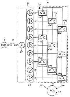
FIG.5 is a circuit diagram showing the first
embodiment of the present invention. The multiple
inverter system shown here comprises a commercial AC
power sauce l, a switch 2, an input transformer 3 having
3n sets of three-phase secondary windings 3P and 1 set of
a primary winding 3S and unit inverter cells 4U1 ~ 4U3,
4V1 ~ 4V3, 4W1 ~ 4W3, which are provided in n (3, here)
stages in order to comprise U, V and W phases of phase
output lines connected to multiple phase load 5.
In FIG S, the secondary windings 3S of the input
transformer 3 are provided in 3 sets of windings in 18
phase structure of which electrical angles are 20 deg.
out of phase each other and each set is connected to the
same stage of the unit inverter comprising each phase.
18b
CA 02249938 1998-10-09
When unit inverters are connected as described above,
the harmonic componets of input currents become the same
without destroying the 18 phase structure even when the
n-th stage of each phase is bypassed.
In FIG S, the zigzag-delta connection of the
secondary windings 3S of the input transformer 3 is shown
butthe zigzag-star connectionis also possible. Further,
according to the first emodiment, when the input
transformer 3 having a plurality of secondary windings 3S
and unit inverters 4U1~4U3, 4V1~4V3 and 3W1~4W3 are
combined , the following actions and effects are obtained.
(1) Output transformers (140, 141 in FIG.1 and
FIG. 2 ) which were so far required are no longer needed
and a high-voltage output is obtained from a small-
sized inverter system.
(2) As the unit inverter cells 4U1~4U3,
4V1~4V3, 4W1~4W3 are used, it is no longer needed to select
serially connected semiconductor devices as before and
as the gate control becomes easier and the circuit voltage
becomes low, the reliability of the system is improved.
(3) As the unit inverter cells 4U1~4U3, 4V1~4V3,
4W1~4W3 are used, in the structure where semiconductor
devices are connected in series, the higher harmonic
component at the output side is decided by PWM switching
frequency of semiconductor and therefore, the reduction
of harmonic wave is restricted naturally, which is so far
19
CA 02249938 1998-10-09
a problem, can be improved.
(4) As the unit inverter cells 4U1~4U3, 4V1~4V3,
4W1~4W3 are used, a trouble that the continuous system
operation becomes impossible if any one f many
semiconductor devices comprising that main circuit, which
was so far a problem, can be improved.
<Second Embodiment>
FIG.6 is a circuit diagram showing the second
embodiment of the present invention and the same reference
numerals as those shown in FIG.5 indicate the same elements.
This circuit differs from FIG.5 in that it is composed of
one set of three-phase inverter 41 and a plurality of
single-phase unit inverters 4U2, 4U3, 4V2, 4V3, 4W2, 4W3.
As other constructions, an input transformer 3
having 3n sets of three-phase secondary winding 3S is
provided, singple-phase inverter cells 4U2, 4U3, 4V2,
4V3,4W2, 4W3 are connected in series for plural stages
(n-1) to construct each phase, which is connected to the
same phase, and the electric power is supplied to the
multiple phase load 5.
FIG.7 shows an example of the circuit of the
three-phase inverter 41 shown in FIG.6. In this circuit,
for instance, self-turn-off semiconducor devices Q1, Q2,
Q3, Q4, Q5, Q6 such as IGBT are bridge connected, diodes
D1 ~ D6 are connected to semiconductors Q1 ~ Q6 in parallel
and thus a three-phase inverter circuit 104 is constructed
CA 02249938 1998-10-09
and terminals 1~5U, 105V, 105W are connected to its output
side. A DC power source 103 is to be connected to the input
side of the three-phase inverter circuit 104. As the
operation of the three-phase inverter circuit is omitted
here as it is well known.
The three-phase inverter 41 and single-phase
inverter cells of the (n-1)th stage connected in-series
are connected with the ~/3n out of phase secondary
windings 3S of the transformer 3.
Thus, the same effect as the embodiment described
above is obtained. In addition, in this embodiment it is
especially possible to reduce the number of unit inverters
and the number of windings of the input transformer 3 and
to make the system small in size.
Further, it is possible that a neutral point clamped
inverter is composed by the unit inverters.
<Third Embodiment>
FIG.8 is a circuit diagram showing the third
embodiment of the present invention. In this circuit,
three input transformers 31, 32, 33 are provided to
in-series connected 3 unit inverter cells 4U1~4U3, 4V1~
4V2, 4W1~4W3 of each phase.
Each of the transformers 31 ~ 33 has 3 sets of ~ /3n
out of phase three-phase windings 31A, 325,
33S at the secondary side and the unit inverter cells
4U1-4U3, 4V1-4V3, 4W1-4W3 at the n-th stage of eac phase
21
CA 02249938 1998-10-09
are connected ~.aith the out of phase secondary windings
31S - 33S at each phase.
3 input transformers (31, 32, 33) are provided for
n (3) in series connected unit inverter cells, each
transformer has 3 sets of ~ / (3X3) out of phase three-
windings at the secondary side and out of phase secondary
winginds are connected to the unit inverter cells at the
n-th stage of each phase. Thus, when the input
transformers 31, 32, 33 are separated, the number of
secondary windings are largely reduced less than when a
systemismanufactured with onetransformerandtherefore,
there is such a merit that fluctuation of impedance
between the windings can be suppressed to a lower level.
So, harmonic component of input current is no longer
fluctuated largely between phases.
<fourth Embodiment>
FIG.9 shows the fourth embodiment of the present
invention. In this embodiment, m units of input
transformer are provided and the secondary winding of each
transformer has 3n sets of three-phase windings. The unit
inverters 4U1~9U2, 4U, 4V1~4V2, 4V, 4W1~4W2, 4W at the n-th
stage of each phase are connected with secondary windings
which are out of phase in each phase.
In the embodiment shown in FIG.9, two transformers
31, 32 are in the entirely same winding construction but
the primary windings 31P, 32P may be made in the star
22
CA 02249938 1998-10-09
connection and the delta connection.
<Fifth Embodiment>
FIG.10 shows the fifth embodiment of the present
invention and the unit inverter cells at the n-th stage
of each phase are connected with the secondary windings
31S, 32S of the same phase input transformers.
In the embodiments shown in FIG.9 and FIG.10, the
design and manufacturing can be simplified by reserving
2 sets for two stages of each phase. In case of the circuit
shown in FIG.7, the circuit can be simplified when it is
constructed with 3 sets by setting with a transformer for
one stage of each phase.
<Sixth Embodiment>
FIG.11 shows the sixth embodiment of the present
invention, characterized in that the the phase of windings
of the primay sides 31P, 32P of the input transformers 31,
32 are shifted by the star and delta connections so as
to make them in the 12 phase structure, the secondary sides
have 3n sets of three-phase windings, respectively and the
secondary windigs of which phases are shifted for each
phase are connected to the unit inverter cells 4U1~4U2,
4U, 4V1~4V1, 4V, 4W1~4W2, 4W. The primary windings of the
transformers of course may be the same.
<Seventh Embodiment>
FIG.12 shows the seventh embodiment of the present
invention and differs from FIG.11 in that the system is
23
CA 02249938 1998-10-09
constructed by connecting the secondary windings of the
same phase at each phase to the unit inverter cells 4U1~4U4,
4V1~4V4, 4W1~4W4 at the n-th stage of each phase.
<Eighth Embodiment>
FIG. 13 is a signal waveform diagam. FIG. 13 (a) shows
the input current to the unit inverter cell when reactance
of the transformer is nearly zero and FIG.13(b) shows
reactance of the transformer that is a proper value so that
the current does not flow intermittently. Generally,
it is easy to manufacture a transformer if % impedance is
10 - 20 0 .
The low order harmonic component of input current
can be improved sharply when such care is paid.
<Ninth Embodiment>
FIG.14 shows the ninth embodiment of the present
invention. Switches 2c~2k that are able to cut off a
circuit are provided at at least either the primary side
or the secondary side three-phase windings of the input
transformer 3 so as to be able to open the corresponding
main power source if the unit inverters 4U1, 4U2a, 4U3a,
4V1, 4V2a, 4V3a, 4W1, 4W2a, 4W3a become faulty.
<Tenth Embodiment>
FIG.15 shows the tenth embodiment of the present
invention. The unit inverter cell comprises a diode
rectifier 102 which converts AC into DC, a smoothing
capacitor 103 and a single-phase inverter circuit 104
24
CA 02249938 1998-10-09
which converts ~C into any frequency AC. When diodes are
used for a rectifier, in order to prevent the rush current
to the capacitor 103, the diodes should be initially
charged for a specified time via a resistor R and
thereafter, a switch SW should be turned ON. In this
embodiment, such self-turn-off semiconductor devices as
GTO, transistor, etc. are used for the single-phase
circuit 104 and such a voltage driving type self-turn-
off device as IGBT, etc. are used in the deformed
embodiment.
<Eleventh Embodiment>
FIG.16 shows the eleventh embodiment of the present
invention and a semiconductor device with a gate control
pole such as thyristor, GTO, etc. are used for the
rectifier 102 which converts AC into DC. In this case,
a circuit 106 whi ch initially charges the DC capacitor 103
shown in FIG.14 can be omitted.
<Twelfth Embodiment>
FIG.17 shows the twelfth embodiment of the present
invention. The rectifier in at least one unit inverter
cell comprises a self-turn-off semiconductor device with
a gate control pole (IGBT, GTO, etc.) and it becomes
possible to make not only the the power factor 1
control( pf=1.0 ) but also particularly the leading
control by the PWM control. In FIG.17, an example of
reactor provided to the input portion is shown to reduce
CA 02249938 1998-10-09
current harmonic. It is also possible to use the reactance
of the input transformer as a reactor without providing
a reactor as described above.
<Thirteenth Embodiment>
FIG.18 shows the thirteenth embodiment of the
present invention, wherein a current driving self-
turn-off semiconductor devices such as GTO are used for
the devices of the inverter circuit 104.
<Fourteenth Embodiment>
FIG.19 shows the fourteenth embodiment of the
present invention, wherein voltage driving self-turn-off
semiconductor devices Q1~Q4 such as IGBT, etc. are used
for the devices of the inverter circuit 104. Further,
FIG.19 shows its deformed example and the output portion
of the inverter circuit of the unit inverter cell is
provided with a switch 104a to bypass its output.
<Fifteenth Embodiment>
FIG.20 (a) and (b) show the output waveforms in this
embodiment and at least one of the inverter circuits of
a plurality of unit inverter cells controls the output
voltage through the PWM control while the other remaining
unit inverters control the output voltage through the PAM
control.
<Sixteenth Embodiment>
FIG.21 shows the sixteenth embodiment and FIG.21 (a)
shows thyristors that are connected antiparallelly,
26
CA 02249938 1998-10-09
FIG.21(b) shows self-turn-off devices such as GTO, etc.
connected antiparallelly and FIG.21(c) shows bridge
connected diodes as a rectifier and a semiconductor device
with a short-circuit control pole S1 connected to its DC
output, and a saturable reactor L1 is connected in series
to this semiconductor device so as to check the current
to rise. FIG.21(d) shows diodes D1, D2 that are bridge
connected using semiconductor devices with a control pole
S1, S2 for use as a switch to bypass the output of the unit
inverter cell so as to short circuit its DC output.
<Seventeenth Embodiment>
FIG.22 shows the seventeeth embodiment and gate
signal phases to the inverter circuit (Q1~Q4 shown in
FIG.14) of the unit inverter cells of U, V, W phases (4U3,
4V3, 4W3) at the third stage shown in FIG.5. When such
phase gate signals are given, the output voltage of the
unit inverter bcomes zero and it is possible to obtain a
low voltage as the output voltage of a multiple inverter
system. The broken lines in FIG.22 shows the operating
waveform in the normal PAM operation.
<Eighteenth Embodiment>
On the other hand, in this embodiment, the output
voltage is controlled to zero by short-circuitting the
output of the unit inverter by operting the bypass circuit
shown in FIG.21. At this time, the gate signal to the
devices of the inverter circuit of the unit inverter cell
27
CA 02249938 1998-10-09
should be suspended.
<Nineteenth Embodiment>
FIG.23 shows the embodimen of the control method.
When controlling the multiple inverter system, as the
harmonic component of the output voltage may increase, it
is possible to supply voltage to a load without increasing
the harmonic component by increasing the PWM operating
frequency (in the embodiment shown in FIG.5, increase PWM
freuqency by 1.5 times) at other stages in operation (other
two stages in FIG. 5). Therefore, the PWM frequency of
the unit inverter cell in operation should be changed by
a bypass command signal or the output voltage zero command.
<Twentieth Embodiment>
FIG.24 shows the twentieth embodiment of the present
invention, wherein switches 401406 capable of changing
over the output voltage are provided between the unit
inverter cells in respective phases of a multiple inverter
system so as to be able to change supply voltage to a
multiple phase load. High-voltage motors are generally
6kV system and 3kV system in Japan and 4.2 kV sysem and
2. 4 kV system in U. S.A. and there are uses to change the
systems according to loads.
<Twenty-First Embodiment>
FIG.25 shows the twenty-first embodiment of the
present invention, wherein the output terminals U1, V1,
W1 and U2, V2, P72 are provided between the unit inverter
28
CA 02249938 1998-10-09
cells in respective phases of a multi-inveter system so
as to be able to change over supply voltage to a multiple
phase load.
<Twenty-Second Embodiment>
FIG.22 shows the twenty-second embodiment of the
present invention, wherein a converter for the
regeneration isconnectedto antiparallellytoa rectifier
of the unit inverter cell at any stage of each phase. In
a system wherein much power is regenerate from load, it
is also easily considered to provide a regeneration
circuit to all unit inverter cells so as to control the
regeneration by any unit inverter cell according to
regenerating volume of power. If a self-turn-off
semiconductor device is used as a regeneration converter,
it is easy to perform the PWM operation and it becomes
possible to precisely control the regenerating power.
<Twenty-Third Embodiment>
FIG.27 shows the twenty-third embodimen of the
present invention, wherein a fault detection and
protective operation circuits of the unit inverter cells
are provided, when the unit inverter cells 4U1~4W3 become
faulty or during the maintenance, the switches 2c~2K
provided to at least either the three-windings of the
primary side or the secondary side of the input
transformers corresponding to the unit inverters at the
n-th stage equivalent to that unit inverter are controlled
29
CA 02249938 1998-10-09
so as to open at lease more than one switch.
<Twenty-Fourth Embodiment>
The output voltage waveform of the twenty-fourth
embodiment of the present invention is as shown in FIG.20
and the control method of the multi-inventor system of the
present invention is in such a structure that at least one
of the unit inverter cells controls its output voltage
through the PAM control and other unit inverter cells
control the output voltage through the PWM control and
voltages in respective phases are serially combined and
the power is supplied to a multiple phase load.
<Twenty-Fifth Embodiment>
The control method of the multiple inverter system
in this embodiment is in such a structure that the
three-phase inverter cells control the output voltage
throuh the PAM control while other unit inverter cells
control the output voltage through the PWM control and
respective phase voltages are serially combined and the
power is supplied to a multiple phase load.
<Twenty-Sixth Embodiment>
FIG.28 shows the PWM control of U-phase on the basis
of the circuit shown in FIG S and the output fundamental
wave phases of the unit inverter cells in respective phases
are controlled by shifig them bye /3n and also, controlled
so that the PWM switching phase at the same phase stage
do not superpose each other. Needless to say, V and W
CA 02249938 1998-10-09
phases are the wave forms of which phases are shifted from
the waveforms shown in FIG.28 by 120°.
<Twenty-Seventh Embodiment>
This embodiment relates to the control of
the mutiple inverter system of the present invention when
starting it as shown in FIG.29, the system is so controlled
that some unit inverter cell is given with a function to
control the current value through the PWM control and when
starting the multiple inverter system, this function is
operated to supply current to the unit inverter cells in
respective phases and after charged the inverter cells to
a preset DC voltage value, the AC power source is turned
ON and the system is operated.
In FIG.29, the rotational speed of a motor 268 is
detected by a rotation detector 269, the detected speed
is fed back and the inverter frequency is so controlled
that it becomes the slip frequency according to a torque
command.
A current control loop (a current control amplifier
266) is provided in many cases. As the slip frequency and
current are jointly controlled at this time, the stability
is satisfactory and the system is endurable to the sudden
acceleration/decelleration orloadfluctuation. Further,
as the detected speed is fed back, accuracy of the
rotational speed is improved.
FIG.29 is a circuit diagram showing what is
31
CA 02249938 1998-10-09
described above and the output of the speed control
amplifier 266 is converted into slip frequency and current
commands which are then converted into the invrter
frequency f, a frequency command and a motor primary
terminal voltage V1 command through respective loops.
There is provided a PWM control circuit for the control
subsequent to a frequency command and a motor primary
terminal voltage V1.
Further, a power regeneration additional circuit is
used for the power rectifier as sudden acceleration /
deceleration is performed. This system is used for a
independent operation as it is required to perform the
closed loop control, and it is possible to generate maximum
torque irrespective of constant output characteristic,
direct winding characteristic and rotational speed. This
circuit comprises a speed setter 260, a comparator 261,
a speed control amplifier 262, a current pattern generator
263, a current detector 264, a comparator 265, a current
control amplifier 266, a PWM control circuit 267, a slip
frequency pattern generator 271, a comparator 272 and a
speed detector 270.
<Twenty-Eighth Embodiment>
FIG.30 shows a diagram of the multiple inverter
system viewed from just the above, showing the twenty-
eighth embodiment of the present invention and when
m-units of input transformers are provided, 3n units of
32
CA 02249938 1998-10-09
the unit inverters are divided into 3n/m, each of which
is combined with one input transformer to one set and m
sets are arranged. That is, by combining an input
transformer 31 and a converter 41 into one set as
illustrated, the economical effect~in designing and
manufacturing can be expected from the same design.
Further, as the dielectric strength also can be reduced
when they are separated, the downsizing of the system
becomes possible. If there are the even number of input
transformers, there are such methods as shown in FIG.30;
a method to arrange two units back to back as in (a), a
method to arrange two units facing each other as in (b)
and a method to arrange two units bisymmetrically from the
center as in (c) and other methods are also considered
according to purpose such as arrangement, maintenance,
improvement of workability.
<Twenty-Ninth Embodiment>
FIG.31 shows the twnety-ninth embodiment of the
present invention. In this embodiment, as the s
impedances of the three-phase secondary windings of 3n
sets are made uniform when comprising secondary windings
of transformers, the windings in respective phases wound
at different locations of a three-phase core are connected
in three phases. Degree of connection of windings of a
transformer generally differs at its inside and outside
and therefore, impedance also varies. In FIG.31, the
33
CA 02249938 1998-10-09
three-phase connection is normally made at the same
locations of u1, v5 and w3 but when three-phase windings
are connected from the locations shown in this figure, it
is possible to make % impedances of transformers uniform,
input current of unit inverter cells can be made equal and
phase currents and harmonic components at the power source
side can be balanced.
Next, the thirtieth embodiment will be described.
<Thirtieth Embodiment>
FIG.32 shows a main circuit of a multi-
inverters (a group of inverters) to be applied with the
present invention, wherein 3 units of U, V and W unit
inverters in three-phase structure are connected; that
is, A24U1, A24U2 and A24U3, A24V1, A24V2 and A24V3, and
A24W1, A24W2 and A24W3. Definitely, fuses A4U1, A4U2 and
A4U3, A4V1, A4V2 and A4V3, and A4W1, A4W2 and A4W3 are
connected in series to the iuput sides of the unit
inverters A24U1, A24U2 and A24U3, A24V1, A24V2 and A24V3,
and A24W1, A24W2 and A24W3, respectively and connected to
a rectifier 2 in parallel with it, and the output sides
of the unit inverters are connected in series for each
phase and connected to a AC load 10, for instance, an
induction motor.
FIG.33 is a block diagram for explaining the
thirtieth embodiment, wherein a bypass circuit only
comprising one unit inverter A9 out of a group of inverters
34
CA 02249938 1998-10-09
(a mutiple inverters) shown in FIG.32, a unit inverter
control means A12 to control the firing of semiconductor
devices A5, A6, A7, A8 of the unit inverter A9, a bypass
switch A11, which is described later, an abnormal
operation detecting means A13, a DC abnormality detecting
means A14, and a bypass switch control means A15
is shown. In actual configuration, there are a
plurlaity of unit inverters A9 and this bypass circuit is
provided to each unit inverter A9.
FIG.34 is a diagram for explaining one example of
the unit inverter control means A12, which feeds back the
rotational speed of an AC motor A68 by detecting it and
controls the inverter frequency so as to make it to the
slip frequency corresponding to a torque command, and is
also provided with a current control loop. Concretely,
the rotational speed of the AC motor A68 is detected by
a rotatio n detector A69 and a speed detector A70, this
detected speed value is compared with a set value of a speed
setter A60 by a comparator A61, a deviation between them
is amplified by a speed control amplifier A62 and the
amplified value is converted into a specified frequency
by a slip frequency pattern generator A71, the converted
frequency is compared with a speed value detected by the
speed detector A70 by a comparator A72 and an inverter
frequency f command thus obtained is applied to a PWM
control circuit A67.
CA 02249938 1998-10-09
The output of the speed control amplifier A62 is
input to a current pattern generator A63, where
it is converted into current, the converted current and
the current detected by a current detecor A64 is compared
by a comparator A65, a deviation obtained by this
comparation is input to a current control amplifier A66
and a motor primary terminal voltage V1 command obtained
here is given to a PWM control circuit A67. The PWM control
circuit A67 gives a gate command corresponding to a ratio
between the inverter frequency f command and the motor
primary terminal voltage V1 command to the gate of each
unit inverter.
In a multiple inverter system in the structure as
described above, if all the unit inverters A9 are in the
properly operable state, the semiconductor devices A5~A8
of the unit inverter A9 are fired and controlled and high
voltage AC power is supplied to the AC load A10.
In this case, as each unit inverter A9 is in the
normal state, the abnormality detecting sinal is not
output from the abnormal operation detecting means A13 and
also, the abnormality detecting signal is not output from
the DC abnormality detecting means A14 at the rectifier
A2 side and therefore, a circuit closing command is not
applied to the bypass switch All from the bypass switch
control means A15. So, the bypass switch All is kept in
the OFF state.
36
CA 02249938 1998-10-09
In such the state where each unit inverter A9 is
proper operating, if, for instance, the semiconductor
devices A5, A8 of one unit inverter A9 is short-circuitted
(however, the bonding wires in IGBT comprising the
unitinverters are still left), such operations as shown
below are carried out . In this case, as AC output current
of the unit inverters A9 increases and/or AC output voltage
drops, the abnormal operation detecting means A13 outputs
a abnormal detecting signal, which is then applied to the
byass switch control means A15.
On the other hand, as DC input current to the
inverter bridge A9 increases, an abnormality detection
signal is output from the DC abnormality detection means
A14 and given to the bypass switch control means A15. As
a result, a circuit close command, that is, a gate ON signal
is given to the bypass switch All from the bypass switch
control means A15. As the bypass switch A11 is then
turned ON, the short-circuit current so far flowing to the
AC load A10 via the semiconductors A5, A8 flows through
the course of the bypass switch All, a fuse A4 and a
smoothing capacitor A3, and the fuse A4 is burnt out. When
the fuse A4 is burnt out, it becomes the output bypass mode
automatically. As a result, the semiconductor devices of
a healthy unit inverter A9 without generating short-
circuit, fault, and the like are fired in the specified
order and the power is supplied to the AC load A10, and
37
CA 02249938 1998-10-09
the AC load A10 can be operated continuously.
Thus, it is not required to stop the operation of
the multiple inverters once to protect AC load from
excessive current resulting from the short-circuit
trouble of unit inverters so far and an AC load A10 can
be operated continuously by the healthy unit inverters A9.
<Thirty-First Embodiment>
FIG.35 is a bock diagram partially showing the
thirty-first embodiment. In FIG.35, likewise FIG.32, one
unit inverter A9, the unit inverter control means A12 which
controls the firing of the semiconductor devices A5, A6,
A7, A8 of the unit inverter A9, and a bypass circuit
comprising the bypass switch All, the abnormal operation
detecting means A13, the DC abnormality detecting means
A14 and the bypass switch control means A15, which will
be described later, only are shown but in the actual
configuration, there are a plurality of unit inveters A9
and each the unit inverters A9 are provided with
above-mentioned bypass circuit, respectively.
FIG.35 differs from FIG.33 only in that an operating
contact A4a which is closed with the burn-out of the fuse
A4 is provided at the input side of the DC abnormality
detecting means A14.
<Thirty-Second Embodiment>
FIG.36 is a block diagram partially showing
the thirty-second embodiment. In FIG.36, likewise FIG.33,
38
CA 02249938 1998-10-09
one unit inverter A9, the unit inverter control means A12
which controls the firing of the semiconductor devices A5,
A6, A7, A8 of the unit inverter A9, and a bypass circuit
comprising the bypass switch All, the abnormal operation
detecting means A13, a level juding means A17 and the
bypass switch control means A15, which will be described
later, only are shown but in the actual configuration there
are a plurality of unit inveters A9 and each of the unit
inverters A9 is provided with the above-mentioned bypass
circuit, respectively.
DC voltage applied to the unit inverters A9 is
detected by the voltage detecting means A16 and the level
judging means A17 detects whether the DC voltage detected
by the voltage detecting means A16 is the overvoltage or
undervoltage against a reference value. When a judging
signal is output from the level judging means A17 and a
detecting signal is output from the abnormal operation
detecting means A13, the bypass switch control means
operates as in FIG.33.
<Thirty-Third Embodiment>
FIG.37 is a block diagram partially showing the the
thity-third embodiment. In FIG.37, likewise FIG.33, one
unit inverter A9, the unit inverter control means A12 which
controls the firing of the semiconductor devices A5, A6,
A7, A8 of the unit inverter A9, and a bypass circuit
comprising the bypass switch A11, the DC abnormality
39
CA 02249938 1998-10-09
detecting means A14, a level juding means A18 and the
bypass switch control means A15, which will be described
later, only are shown but in the actual configuration,
there are a plurality of unit inveters A9 and each of the
unit inverters A9 is provided with above-mentioned bypass
circuit, respectively.
The level judging means 18 detects the abnormality
when the output voltage of the unit inverter A9 detected
by the voltage detecting means A25 exceeds the specified
range against a reference value. When a judging signal
is obtained from the level j udging means 18 and a detecting
signal is output from the DC abnormality detecting means
A14, a circuit closing command is output from the bypass
control means A15 to the bypass switch All as in FIG.33.
<Thirty-Fourth Embodiment>
FIG.38 is a block diagram partially showing the
thirty-fourth embodiment. In FIG.38, likewise FIG.33,
one unit inverter A9, the unit inverter control means A12
which controls the firing of the semiconductor devices A5,
A6, A7, A8 of the unit inverter A9, and a bypass circuit
comprising the bypass switch All, the output deetecting
means A35, A36, A37, A38, the inverter output detector A19
and the abnormal judging means A20, which are described
later, only are shown but in the actual configuration,
there are a plurality of unit inveters A9 and each of the
unit inverters A9 is provided with the above-mentioned
CA 02249938 1998-10-09
bypass circuit.
FIG.38 differs from FIG.33 in that the abnormal
judging means 20 inputs the output voltage detected by the
inverter output detector A19 and the voltage detected by
any one of the output detectors A35-A38 of the unit
inverter control means A12 and detects a fault resulting
from the abnormality of the unit inverter control means
A12, that is, an external factor from the relationship of
both voltages.
<Thirty-Fifth Embodiment>
FIG.39 is a block diagram partially showing the
thirty-fifth embodiment. In FIG.39, likewise FIG.33, one
unit inverter A9, the unit inverter control means A12 which
controls the firing of the semiconductor devices A5, A6,
A7, A8 of the unit inverter A9, and a bypass circuit
comprising the bypass switch All, the output detecting
means A35, A36, A37, A38 and the abnormality judging means
A21 only, which are described later, are shown but in the
actual configuration, there are a plurality of unit
inveters A9 and each of the unit inverters A9 is provided
with the above-mentioned bypass circuit.
FIG.39 differs from FIG.38 only in that the voltage
with volage wave detected by the output detecting means
A35~A38 is input to the abonomality judging means 21, and
abnomality based on an external factor is judged by
comparing this voltage wave with a refernce voltage wave.
41
CA 02249938 1998-10-09
<Thirty-Sixth Embodiment>
FIG.40 is a block diagram partially showing the
thirty-sixth embodiment. In FIG.39, likewise FIG.33, one
unit inverter A9, the unit inverter control means A12 which
controls the firing of the semiconductor devices A5, A6,
A7and A8 of the unit inverter A9, and a bypass circuit
comprising the bypass switch All, the abnormality judging
means A21 and the power source abnormality detecting means
A22 only, which are described later, are shown but in the
actual configuration, there are a plurality of unit
inveters A9 and each of the unit inverters A9 is provided
with the above-mentioned bypass circuit.
FIG.40 differs from FIG.38 in that the power source
abnormality detecting means A22 detects the power source
abnormality of the unit inverter control means A12 , inputs
this detected ouput to the abnormality judging means A21
and by comparing this detected output wih a reference
voltage, judges the abnormality by an external factor.
<Thirty-Seventh Embodiment>
In FIG.32, it is needless to say that as the
configuration of multiple inverters, U, V and W phase
inverters A24U1, A24U2, A24U3, A24V1, A24V2, A24V3, A24W1,
A24W2 and A24W3 are combined by 3 units and connected each
other and fuses A4U1, A4U2, A4U3,A4V1, A4V2, A4V3, A4W1,
A4W2 and A4W3 are connected to each unit inverter likewise
the embodiments described above and in addition, a bypass
42
CA 02249938 1998-10-09
circuit in the same structure as in the embodiments
described above is provided to each unit inverter.
<Thirty-Eighth Embodiment>
FIG.41 and FIG.42 are diagrams for explaining the
thirty-eighth embodiment of the present invention.
FIG. 41 shows that the main circuit is a three-phase circuit
as in FIG.32 and partially shows the PWM control circuit
A67 shown in FIG.34, A29 shows a reverse dq converter and
A30, A31 and A32 show proportional computing units.
In such the structure as described above, when one
unit inverter becomes faulty for short-circuit, etc. and
the operation is continued by the reamining healthy unit
inverters, the modulation factor of the unit inverter in
a phase causing above-described abnormality is increased
to more than one time.
The output voltage waveforms in respective phases
of a multiple inverters in this case are shown in FIG.42
and it is possible to compensate the output voltage drop
of a group of inverters in respective phases resulting of
decrease of unit inverters.
<Thirty-Ninth Embodiment>
In a multiple inverter system in the same structure
as in FIG.38, in the main circuit shown in FIG.32, the
number of unit inverters in the healthy phase are operated
corresponding to, for instance, the number of unit
inverters in the phase detected by each abnormal operation
43
CA 02249938 1998-10-09
detecting means A13.
<Deformed Example>
In the above embodiments, a case where such
semiconductor switch as a thyristor was used as a bypass
switch All was exlained but a mechanical switch may be used
instead of a semiconductor switch. A mechnical switch has
a smaller thermal loss than a semiconductor switch;
however, on the other hand, as the operation is slower than
a semiconductor switch, it is not possible to continuously
operate by protecting while operating.
In the above embodiments, a case where all of unit
inverters in each phase are operated when the inverters
are properly bridged was explained. When the inverter
bridge is proper, at least one of unit inverters of each
phase may be used as a standby inverter. In this case,
unit inverters of respective phases that are operated and
those not operated as standby inverters are automatically
selected or manually selected by operator using, for
instance, a copper bar.
Further, semiconductor devices comprising unit
inverters are explained by taking IGBT as an example in
the above embodiments, antiparallelly connected
thyristors shown in FIG.43(a) or antiparallelly connected
GTOs shown in FIG.43(b) are usable. Further, a series
circuit comprising a semiconductor device AS1 with a
short-circuit control pole and a saturable reactor AL1 may
44
CA 02249938 1998-10-09
be connected to the diode bridge output side as shown in
FIG. 43 (c) . In addition, as shown In FIG. 43 (d) , the system
may be constructed using the bridge connected diodes AD1,
AD2 and semiconductor devices with a control pole AS1, AS2
as a bypass switch to bypass the output of the unit inverter
A9 so as to short circuit its DC output.
According to the present invention described above,
by combining transformers having secondary windings with
unit inverters, it is possible to provide a small-sized
economical multiple inverter system andits control method
capable of obtaining high-voltage output, reducing higher
harmonic to load side and also, reducing harmonic current
of a power source system swithout requiring output
transformers.
In addition, according to the present invention, it
is possible to provide a multiple inverter system capable
of continuouly operating AC load even when short-circuit,
other troubles are caused on at least one of unit inverters
without suspending the operation of remainng healthy unit
inverters.
Obviously, numerous additional modifications and
variations of the present invention are possible in light
of the above teachings . It is therefore to be understood
that within the scope of the appended claims, the invention
may be practiced otherwise than as specially described
herein.