Note: Descriptions are shown in the official language in which they were submitted.
CA 02249977 1998-09-23
Specification
Image Sensor Chip and Image Sensor
Technical Field
The present invention relates to an image sensor chip for
reading an image of a scanned object, and an image sensor
comprising a plurality of the image sensor chips.
Background Art
According to a prior art image sensor chip, image signals
from a plurality of photoelectric elements are serially output
from an output pad without being amplified. A prior art image
sensor comprising a plurality of such image sensor chips has
an amplifying circuit formed on an amplifying circuit board
separate from an image sensor chip board. The image signals
from each of the image sensor chips are supplied to the
amplifying circuit via a wiring pattern and a connector of the
image sensor chip, and a wiring pattern of the amplifying
circuit. After the signals are amplified by the amplifying
circuit, the signals are serially output via the wiring pattern
of the amplifying circuit, a connector and other components
to an external circuit.
However, according to the prior art, the image signals from
each of the image sensor chips are supplied to the amplifying
circuit only after passing through the wiring pattern and the
connector of the image sensor chip, and the wiring pattern of
the amplifying circuit. Therefore, the signals are subject
1
CA 02249977 1998-09-23
to noise, and it was difficult to obtain accurate image signals
of an original image. Specifically, the image signals have
a small voltage whereas the amplifying circuit has a large input
impedance. As a result, noise can enter easily, and may become
very large if there is a long path between the image sensor
chip and the amplifying circuit. Especially, if there is such
an apparatus as a laser printer located near by, the image
signals can be badly affected by the noise from the laser
printer.
This problem may be solved for example, by encasing the
image sensor in a structure made of metal such as aluminum.
However, this method of electromagnetically shielding the
internalcircuitry of the imagesensor increases manufacturing
cost of the image sensor.
Another option for solution may be providing each of the
image sensor chips with a built-in amplifying circuit so that
each image sensor chip can output amplified image signals.
With such an arrangement, however, the amplifying circuit
built in each of the image sensors will have different offset
from each other, making difficult to obtain accurate image
signals of an original image. This problem is particularly
serious in image sensing of a colored or gradated image because
the difference in offsets can easily result in difference in
the gradation or color.
This problem may be solved by adding a correction circuit
for correcting the differences in the offsets. The correction
circuit may be added to an image signal processing circuit which
processes the image signals after the signals are output from
2
CA 02249977 1998-09-23
the image sensor. However, this arrangement increases
manufacturing cost of the apparatus which includes the image
sensor.
Another option for solution may be providing one of the
image sensor chips of each row with a built-in amplifying
circuit so that image signals from all of the image sensor chips
of that row can be amplified by this amplifying circuit before
output to an external circuit.
This arrangement can solve the problem of the difference
in offset within each row. In addition, there will be less
problem of noise than in the case where the amplifying circuit
is made separately on the amplifying circuit board. With this
arrangement, however, two types of image sensors must be
manufactured for mounting on an image sensor chip board. This
decreases advantages of mass production in manufacture of the
image sensor chips. Further, a more complex procedure must
be used for mounting the image sensor chips on the image sensor
chip board, increasing manufacturing cost of the image sensor.
As exemplified above, each of the three methods has
advantages and disadvantages. Preferably therefore, any of
the three methods should be selectively usable depending upon
application of the image sensor. However, manufacturing
different types of image sensors for each method will further
decrease the advantages of mass production in the manufacture
of image sensor chips, increasing further the manufacturing
cost of the image sensor.
3
CA 02249977 1998-09-23
Disclosure of the Invention
It is therefore an object of the present invention to
provide an image sensor which can selectively take an output
mode of, outputting image signals without amplification,
outputting image signals amplified by an amplifying circuit
built for each of the image sensor, or outputting image signals
amplified by an amplifying circuit provided in each row of the
image sensor chips, by means of wirebonding at the time of
manufacture.
Another object of the present invention is to provide an
image sensor chip for such an image sensor.
According to a first aspect of the present invention, there
is provided an image sensor chip comprising a plurality of
photoelectric elements for converting light reflected by a
scanned object into analog image signals, a selecting circuit
for sequential takeout of the serial image signals from
respective output terminals of the photoelectric elements, a
first pad for output of the image signals taken out serially
by the selecting circuit, an amplifying circuit capable of
amplifying the image signals from the plurality of
photoelectric elements, a second pad connected to an input
terminal of the amplifying circuit, and a third pad connected
to an output terminal of the amplifying circuit.
With the above arrangement, image signals before
amplification can be obtained by taking image signals from the
first pad. Image signals after amplification can be obtained
by entering image signals from the first pad into the second
pad, and then taking the image signals from the third pad.
4
CA 02249977 1998-09-23
Further, other image sensor chips having the same construction
may have image signals from their respective first pads entered
commonly into the second pad. Then, by taking image signals
from the third pad, amplified image signals from the plurality
of image sensor chips can be obtained. Thus, by using a
plurality of this image sensor chip, it becomes possible
without increasing the manufacturing cost, to provide the
image sensor which can selectively take an output mode of,
outputting image signals without amplification, outputting
amplified image signals, or outputting image signals amplified
by another image sensor chip, by means of wirebonding at the
time of manufacture.
The object to be scanned may be an image on a piece of paper
or a film of resin, or the image may not necessarily be on a
sheet material.
The photoelectric element may be but not limited to a
photodiode or a phototransistor.
The selecting circuit may be but not limited to a shift
register or a CCD.
The amplifying circuit may be but not limited to an
operational amplifier.
An image sensor chip according to the preferred mode of
embodiment further comprises a first switching circuit
operated by external control signals for switching between a
state in which the image signals from the selecting circuit
are supplied to the first pad and another state in which the
image signals are not supplied to the first pad, and a second
switching circuit operated by external control signals for
5
CA 02249977 1998-09-23
switching between a state in which output signals from the
amplifying circuit are supplied to the third pad and another
state in which the output signals from the amplifying circuit
are not supplied to the third pad.
With the above arrangement, the first or the second switch
circuit may be opened when the respective first or third pad
is not used for obtaining the image signals or the amplified
image signals. Thus, the transfer path of the image signals
can be effectively protected from noise entering into the
circuit or being output from the first or third pad. This makes
possible to maintain a good reading performance, and is
especially advantageous in eliminating a noise from entering
the amplifying circuit and then being output from the third
pad as a big noise.
Each of the first and second switching circuits may be made
by but not limited to a field effect transistor.
According to a second aspect of the present invention,
there is provided an image sensor comprising a wiring substrate
provided with at least one row of image sensor chips described
above. The wiring substrate comprises a first wiring pattern
common to said at least one row of sensor chips, a second wiring
pattern common to said at least one row of sensor chips, and
a third wiring pattern provided individually for each of the
image sensor chips in said at least one row.
According to the above arrangement, it becomes possible
to manufacture an image sensor which outputs image signals
without amplification, an image sensor which outputs image
signals amplified by an amplifying circuit built in each of
G
CA 02249977 1998-09-23
the image sensor chips, or an image sensor which outputs image
signals amplified by an amplifying circuit provided in each I
row, from a common set of the image sensor chips and the wiring
substrate board, only by changing the wirebonding pattern.
Since there is no need for preparing plural types of substrate
boards having different wiring patterns, the manufacturing
cost can be further decreased.
According to a first wirebonding mode, the first pad of
each image sensor chip is wirebonded to the first wiring pattern,
so that image signals from said at least one row of the image
sensor chips are output serially via the first wiring pattern.
According to a second wirebonding mode, the first and
second pads of each image sensor chip are wirebonded to the
corresponding third wiring pattern, whereas the third pad of
each image sensor chip is wirebonded to the first wiring pattern,
so that image signals from said at least one row of the image
sensor chips are amplified by respective amplifying circuits
for serial output via the first wiring pattern.
According to a third wirebonding mode, the wiring
substrate further has a fourth wiring pattern for selected one
of the sensor chips of said at least one row of the image sensor
chips. The first pad of each image sensor chip is wirebonded
to the second wiring pattern. The second pad of the selected
image sensor chip is also wirebonded to the second wiring
pattern. The third pad of the selected image sensor chip is
wirebonded to the first wiring pattern. Further, the selected
image sensor chip has a fourth pad which is wirebonded to the
fourth wiring pattern, so that image signals from said at least
CA 02249977 1998-09-23
one row of the image sensor chips are amplified by the
amplifying circuit of the selected image sensor chip for serial
output via the first wiring pattern.
Other objects, features and advantages of the present
invention will become clear from detailed description
hereafter to be made referring to the attached drawings.
Brief Description of the Drawings
Fig. 1 is an explosive perspective view of an image sensor
according of a first embodiment of the present invention.
Fig. 2 is a partial plan view of the image sensor.
Fig. 3 is a sectional view taken on lines III - III in Fig.
1.
Fig. 4 is a sectional view taken on lines IV - IV in Fig.
1.
Fig. 5 is a sectional view taken on lines V - V in Fig.
1.
Fig. 6 is a circuit diagram showing a first example of
wiring pattern for the image sensor chip.
Fig. 7 is a circuit diagram showing a second example of
wiring pattern for the image sensor chip.
Figs . 8 and 9 respectively show a circuit diagram showing
a third example of wiring pattern for the image sensor chip.
Best Mode for Carrying Out the Invention
A preferred embodiment of the present invention is
described specifically with reference to the accompanying
drawings.
8
CA 02249977 1998-09-23
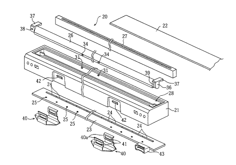
Referring to Figs. 1 through 5, an image sensor 20
according to the embodiment of the present invention comprises
a long case 21 having a predetermined length and a generally
rectangular cross section. The case 21 can be molded of resin
for example. As clearly shown in Fig. 3, the case 21 has an
inner space as a perpendicular through hole, with a glass cover
22 sealing an upper opening, and a head substrate 23 sealing
a bottom opening. The bottom substrate 23 has an upper surface
mounted with a plurality (or specifically 18 according to the
illustrated embodiment) of image sensor chips 24 along a
longitudinal edge of the surface. On the same surface of the
head substrate 23, and along the other longitudinal edge, a
plurality of LED chips 25 are provided. The inner space of
the case 21 includes a light guide 26 made of a transparent
resin for directing the light from the LED chips 25 to a document
D on the glass cover 22, and a rod lens array 27 for collecting
light reflected by the document D on the image sensor chips
24 without magnification nor inversion.
The rod lens array 27 is inserted from above and held by
a grooved holding portion 28 formed in the case 21 . The grooved
holding portion 28 has a holding groove 29 corresponding to
the plan view shape of the rod lens array 27, and a bottom
portion formed with a slit 30 for allowing the light from the
rod lens array 27 to pass through to the image sensor chips
24.
As shown in Fig. 3, the grooved holding portion 28 has
a long inner wall. A longitudinally intermediate portion of
the inner wall is formed with a pair of projections 31 for
9
CA 02249977 1998-09-23
engaging with an upper face of the rod lens array 27 so that
the rod lens array 27 will not spontaneously come up. Each
of the projections 31 has an appropriate height, and is formed
with a tapered upper face 31a so as not to interfere with the
rod lens array 27 when the rod lens array is inserted into the
grooved holding portion 28.
The light guide 26 is a prism for introducing the light
from the LED chips 25 efficiently to and around a reading line
L. The reading line L is disposed on an optical axis of the
rod lens array 27 whereas the LED chips are disposed away from
the axis on the head substrates 23 . The light guide 26 is fitted
in a space enclosed by an inner side wall 21a of the case 21,
a side wall 28a of the grooved holding portion 28, and a bottom
wall 33. The bottom wall is formed with a window 32 facing
the LED chips 25.
As shown in Fig. 1, the light guide 26 has a longitudinal
side face with an intermediate portion formed with a couple
of engaging projections 34. Further, the inner side wall 21a
of the case 21 is formed with corresponding engaging recesses
35 for engaging with the projections 34. As shown in Figs.
1 and 5, the light guide 26 has end portions each formed with
a fitting block 36 of a predetermined size for fitting between
the inner side wall 21a of the case and the side wall 28a of
the grooved holding portion 28. Each of the fitting block 36
is formed integrally with an extending presser segment 37 for
pressing a corresponding end portion of the rod lens array 27
from above. One of the fitting blocks 36 has a back face formed
with a projection 38 whereas the other fitting block has a back
CA 02249977 1998-09-23
face formed with a rib 39 for holding respective fitting blocks
36 firmly by increased friction when fitted between the inner
wall 21a of the case and the side wall 28a of the grooved holding
portion.
The image sensor 20 of the above arrangement can be
assembled in the following steps. Specifically, the rod lens
array 27 is inserted from above into the grooved holding portion
28 in the case 21. In this step, each of the engaging
projections 31 formed in the inner wall of the grooved holding
portion 28 engages with the upper face of the rod lens array
27 so that the rod lens array 27 will not spontaneously come
up.
Next, the light guide 26 is fitted from above into the space
enclosed by the inner side wall 21a of the case and the side
wall 28a of the grooved holding portion. In this step, each
of the engaging projections 34 formed in the light guide 26
engages with the corresponding recess 35 of the case 21, and
each of the fitting blocks 36 fits into the space, holding the
light guide firmly into the space. Further, each of the
presser segments 37 extending from the fitting block 36 of the
light guide 26 presses from above the corresponding end portion
of the upper face of the rod lens array 27. Thus, the rod lens
array 27 is pressed at its longitudinally intermediate
portions by the engaging projections 31, and at its
longitudinally end portions by the presser segments 37, being
held stably and firmly at the predetermined position.
The glass cover 22 is fitted by bonding for example, into
the upper opening of the case 21. The head substrate 23 is
11
CA 02249977 1998-09-23
fitted into the bottom opening of the case 21 and is fixed by
metal clamps 40. As shown in Fig. 4, each of the clamps 40
is a generally U-shaped piece of spring steel with each of its
leg portions 40a formed with an engaging hole 41 for engaging
with a corresponding engaging projection 42 formed on
corresponding outer side faces of the case 21.
The image sensor chips 24 ( 18 chips ) are disposed on the
head substrate in a row at a predetermined interval from each
other. Each of the image sensor chips 24 has 96 photoelectric
elements, and hence a total of 1728 photoelectric elements are
involved in reading a line. The head substrate 23 is provided
with a connector 43 for signal communications with the image
sensor 20.
As shown in Fig. 6, each of the image sensor chips 24 has
96 phototransistors(PHT). Each of these PHT's has its
collector connected commonly to a power source vDD, whereas
its emitter is connected to a drain of a corresponding first
field effect transistor FET1. Each of the first field effect
transistors FET1 has a gate connected to a corresponding bit
of a shift register SR. The first field effect transistor FET1
also has a source connected commonly to a drain of a second
field effect transistor FETz which constitutes a first
switching circuit. The shift register SR has an input terminal
connected to a pad SI which receives serial-in signals. The
second field effect transistor FETz has a gate connected to
a pad CSEL for receiving chip-select signals supplied
externally as control signals, and to one input terminal of
an "or" circuit OR. The second field effect transistor FETz
12
CA 02249977 2000-12-28
has a source connected to a first bonding pad 1. The shift
register SR and the first field effect transistors FET1
constitute a selecting circuit for sequentially taking image
signals out of respective output terminals of the plurality
of phototransistors.
The first bonding pad 1 is adjoined by a second bonding
pad 2. The second pad 2 is connected to a non-inverting
input terminal of an operational amplifier OP, which
constitutes an amplifying circuit, an end of a resistor R1,
and an end of a capacitor C. The other end of resistor R1
and capacitor C are grounded respectively. An inverting
input terminal of the operational amplifier OP is connected
to an end of a resistor R2 and an end of a resistor R3. The
other end of the resistor R2 is grounded, whereas the other
end of the resistor R3 is connected to an output terminal of
the operational amplifier OP and the drain of the third field
effect transistor FET3 which constitutes a second switching
circuit. The third field effect transistor FET3 has a source
connected to a third bonding pad 3. The third field effect
transistor FET3 also has a gate connected to the output
terminal of the "or" circuit OR. The other input terminal of
the "or" circuit OR is connected to a fourth bonding pad 4
and one end of the resistor R4, with the other end of the
resistor R4 being grounded.
The head substrate 23 has an upper surface formed with a
first wiring pattern 6 which is a common wiring pattern wired
to a connector 43 disposed on the head substrate 23 adjacent
to the image sensor chips 24, a second wiring pattern 7 which
is a common wiring pattern formed adjacent to the first
wiring
13
CA 02249977 1998-09-23
pattern 6; and a third wiring pattern 8 which is made of a
plurality of individual wiring patterns formed adjacent to the
first and second pads l, 2.
The first through fourth pads 1,2,3,4 are selectively
wirebonded to the first through third wiring patterns 6, 7 or
8. By changing the pattern of wirebonding, the mode of image
signal output from the image sensor 20 can be changed.
For example, as shown in Fig. 6, the first pad 1 of each
of the image sensor chips 24 may be connected to the first wiring
pattern 6 via a wire 10. In this case, image signals from the
phototransistors PHT go through their respective first field
effect transistors FET1, the second field effect transistor
FET2 , first pad 1, wire 10 , first wiring pattern 6 , and connector
43 before being output from the image sensor 20 . In other words,
the image signals are output from the image sensor 20 without
being amplified by the operational amplifier OP.
Circuit operation for serial output of image signals will
be described here only briefly since this is public
information: One of the image sensor chips 24 is selected by
a chip-select signal. The chip-select signal turns on the
second field effect transistor FETz of the selected image
sensor chip 24, making the first pad 1 ready to receive image
signals. Then, a serial-in signal is entered to the shift
resistor SR. The serial-in signal is shifted in
synchronization with a clock signal. This sequentially turns
on the first field effect transistors FET1 connected to
respective bits at each stage of the shift register SR so that
image signals are output in series. Such a cycle of operation
14
CA 02249977 1998-09-23
is sequentially made for each of the image sensor chips 24 so
the total of 1728 image signals from one line can be output
in series.
As shown in Fig. 7, each of the image sensor chips 24 may
be wirebonded so its first pad 1 is connected to the third wiring
pattern 8 via a wire 11, whereas its second pad 2 is connected
to the third wiring pattern 8 via a wire 12, and its third pad
3 is connected to the first wiring pattern 6 via a wire 13.
In this case, image signals from the phototransistors PHT go
through their respective first field effect transistor FET1,
the second f field ef f ect trans istor FETz , f first pad 1, wire 11,
third wiring pattern 8, wire 12, and second pad 2 before
entering into the non-inverting input terminal of the
operational amplifier OP. Then, the image signals are
amplified by the operational amplifier OP, and goes through
the third field effect transistor FET3, third pad 3, wire 13,
first wiring pattern 6 and connector 43 before being output
from the image sensor 20. In other words, the image signals
after being amplified by the operational amplifier OP mounted
in each of the image sensor chips 24 are output from the image
sensor 20.
Further, an arrangement may be made as shown in Fig. 8,
for a left-end image sensor chip 24 for example, of the total
of 18 image sensor chips 24 . A fourth wiring pattern 9 is formed
adjacent to the fourth pad 4. Of this particular image sensor
chip, the first pad 1 is connected to the second wiring pattern
7 via a wire 14, the second pad 2 is connected to the second
wiring pattern 7 via a wire 15 , and the fourth pad 4 is connected
CA 02249977 1998-09-23
to the fourth wiring pattern 9 via a wire 16. For the rest
of the image sensor chips 24, as shown in Fig. 9, each of the
first pad 1 is connected to the second wiring pattern 7 via
the wire 14. In this case, image signals from the
phototransistors PHT of said rest of the image sensor chips
24 go through their respective first field effect transistor
FET1, the second field effect transistor FETz, first pad 1, wire
11, and wire 14 before entering into the second wiring pattern
7. Then, these image signals go through the wire 15 into the
second pad 2, are amplified by the operational amplifier OP,
and then go through the third field effect transistor FET"
third pad 3 , wire 13 , f first wiring pattern 6 and connector 43
before being output from the image sensor 20. Meanwhile, in
the left-end image sensor chip 24, the "or" circuit OR has its
other input terminal supplied with power VDD via the fourth
wiring pattern 9, wire 16, and the fourth pad 4. As a result,
the third field effect transistor FET3 stays turned on even
when there is no chip-select signal supplied to the relevant
input terminal. In other words, the image signals from each
of the image sensor chips 24 are amplified by the operational
amplifier OP mounted in the left-end image sensor chips 24,
and then output from the image sensor 20. It should be noted
that the fourth wiring pattern 9 is only formed adjacent to
the fourth pad 4 of the left-end image sensor chip 24.
According to the embodiment described above, the image
sensor chips 24 are disposed in a single row on the head
substrate 23. Alternatively however, the image sensor chips
24 may be disposed in a plurality of rows on the head substrate
1G
CA 02249977 1998-09-23
23 with each row provided with the wiring patterns 6 through
8 formed near by. This arrangement provides a plane-image
sensor. with this arrangement, the first wiring pattern 6 of
each row may be individually wired to the connector 43 for
parallel output of the image signals from each of the image
sensor chips 24. Alternatively, the first wiring pattern 6
of each row may be combined into a single wiring pattern, and
then wired to the connector 43 so that the image signals from
all of the image sensor chips 24 are output serially from the
image sensor.
lr