Note: Descriptions are shown in the official language in which they were submitted.
CA 02250496 1998-09-23
WO 98/34215 PCT/US98/01699
SPl~ECH AND SOIJI'~D SYNTHESIZING
Reference to Ap~endices
Text Appen~ires A-D are being submitted with the ~.e3_"t
applir~t.O~
Back~round of the Invcntion
The present invention relates in general to speech and sound
synthesi7ing circuits and more particularly concems techn~ues for
combining high-~ffiri~nry LPC speech syntheci~in~ chips with the low-cost
memory of ADPCM audio syntheci~ine chips.
One e~mple of LPC (linear preclictive coding) speech syntheci7ing
chips is the Te~cas Instruments TSP50CXX f~mily of LPC chips. These chips
are highly efficient in their use of stored speech data because their speech
syntheci~r models a tube of resor~nt cavities corresponding to the human
vocal cords, mouth, etc. Thus, these chips can synthesize speech at a low
data rate. TSP50C~ chips are described in the Texas Instruments Design
Manual for the TSPSOCOXI 1X Family Speech Synthesizer and also irn U.S.
Patents Nos. 1,234,761, 4,449,233, 4,335,275, and 4,970,659.
An e~cample of ADPCM (adaptive pulse code mod~ tion) audio
sYnthesizing chips is the Sunplus SPC40A, SPC256A, and SPC5 12A family
of chips. These chips produce speech and other sounds at a high data rate.
The chips provide low-cost memory because the chips compele with the
LPC chips on a cost-per-secor~'l basis, and given that their data usage rate
is higher than that of the LPC chips by an order of magnitude, these chips
must therefore be designed to achieve a cost per memorv element that is
lower than that of the LPC chips by an order of magnitude. In addition,
these chips do not include comple~c speech S~ thecic circuitry.
Summarv of the Invention
One aspect of the invention features a speech synthesizing circuit
that includes a speech svnthesizing integrated c*cuit chip and an external
CA 02250496 1998-09-23
W O 98/34215 PCT~USg8/01699
memory integrated circuit chip. The speech synthe~i~ing integrated circuit
chip includes a microprocessor, a speech synthesizer, a progr~mm~hle
memory, an input/output port, and a speech address register for storing an
address cont~inin~ speech data. The speech synthesizing integrated circuit
chip includes an instruction, pre-programmed into the speech synthesi~in~
integrated circuit chip during manufacture thereof, that c~ll.ses an address
to be loaded onto the speech address register. The input/output port of the
speech synthesizing integrated circuit chip is connected to the external
memory integrated circuit chip. The progr~mm~hle memory of the speech
synthesi7:ing integrated circuit chip is programmed to cause the
microprocessor to retrieve speech data from the external memory integrated
circuit chip for speech synthesis by the speech synthesizer. The
progr~mm~hle memory is programmed by providing a software simulation of
the instruction that causes an address to be loaded onto the speech address
register. The software simulation causes the address to be loaded into the
external memory integrated circuit chip.
In certain embodiments the external memory is an audio data
storage memory of an audio synthesizing integrated circuit chip that could
not ordinarily interface directly with the speech synthesizing integrated
circuit chip. The software simulation makes it is possible to retrieve speech
data from a preferably relatively inexpensive e~cternal memory without the
use a hardware interface, thereby minimi~ing overall cost. The minimi~tion
of cost is especially important in certain electronic toys.
According to another aspect of the invention, the speech
synthesi7:ing integrated circuit chip includes one or more instructions, pre-
programmed into the speech synthesizing integrated circuit chip during
manufacture thereof, that obtain speech data located at an address stored
CA 022~0496 1998-09-23
WO 98134215 PCT/US98/01699
in the speech address register. At least one of the integrated circuit chips is
programmed to cause speech data to be delivered from the external memory
integrated circuit chip to the speech synthesizing integrated circuit chip for
speech synthesis by the speech synthesizer, by providing a software
simulation of the one or more instructions that obtain speech data located
- at an address stored in the speech address register. The software
simulation causes speech data to be obtained by the speech synthesizing
integrated circuit chip from the external memory integrated circuit chip at
an address stored in the external memory integrated circuit chip.
According to another aspect of the invention, the speech
synthe~i~ing integrated circuit chip includes a linear predictive coding ~LPC)
speech synthesizer and the external memory is the audio data storage
memory of an audio synthesizing integrated circuit chip that also includes a
microprocessor, an adaptive pulse code modulation (ADPCM) synthesizer, a
progr~mm~hle memory, and an input/output port. The progr~mm~hle
speech data retrieved from the audio data storage memory of the audio
synthesizing integrated circuit chip by the speech synthesizing integrated
circuit chip is used for speech synthesis by the speech synthesizing
integrated circuit chip.
In certain embodiments the programmable memory of the audio
synthesizing inte~srated circuit chip is progr~nlmed to cause the
microprocessor of the audio synthesizing integrated circuit chip to retrieve
audio data (e.g., data for non-speech sounds such as breaking glass, ringing
bells, etc.) from the audio data storage memory of the audio synthesizing
integrated circuit chip for audio synthesis by the audio synthesizer of the
audio synthesizing integrated circuit chip. In other embodiments the audio
data from the audio synthesizing integrated circuit chip is delivered to the
speech synthesizing integrated circuit chip for speech synthesis by the
speech synthesizer.
CA 022~0496 1998-09-23
WO 98/34215 PCT/US98/01699
The ability to combine the LPC speech synthesizing integrated
circuit chip and the ADPCM audio synthesizing integrated circuit chip is
useful in certain electronic toys, in which the speech synthesizing integrated
circuit chip produces speech while the audio synthesizing integrated circuit
chip produces non-speech sound effects. The sharing of speech data
between the two integrated circuit chips can be an efficient way to take
advantage of a preferably relatively inexpensive memory on the audio
synthesizing integrated circuit chip and a preferably relatively efficient
speech generation algorithm used by the speech synthesizing integrated
circuit chip. This makes it possible to provide e~ctended speech at low cost.
According to another aspect of the invention, one of the integrated
circuit chips includes a balanced speaker driver having two outputs for
connection of a first speaker impedance between the two outputs, and
another of the integrated circuit chips includes a single-ended speaker
driver having a single output for connection to a second speaker impedance.
A speaker is connected between the two outputs of the balanced speaker
driver of the first audio synthesizer and is also connected to the single-
ended speaker driver of the second audio synthesizer.
The connection of a single speaker to the balanced speaker driver
and the single-ended speaker driver (with the use of an appropriate
resistance network to ensure that each driver "sees" an appropriate effective
resistance to which it is connected) makes it possible to combine audio
effects from both integrated circuit chips (for e~cample, speech from one chip
and non-speech sound effects from the other chip) with a single speaker,
thereby minimi?ing cost. This minimi~tion of cost is important in certain
electronic toys. The audio effects from the two integrated circuit chips can
be combined simultaneously if the balanced speaker driver produces a
pulse width modulated output while the single-ended speaker driver
produces an analog output.
CA 02250496 1998-09-23
WO 98134215 PCTtUS98/01699
Numerous other features, objects, and advantages of the invention
will become apparent from the following detailed description when read in
cormection with the accompanying drawings.
Brief Description of the Drawin~s
FIG. l is a functional block diagram of the Te~as Instruments
TSP50CXX family of speech synthesizing chips.
FIG. 2 is a block diagram of a Texas Instruments TSP50ClX
speech synthesizing chip interfaced with an external memory chip through a
Texas Instruments TMS60C20-SE hardware interface chip.
FIG. 3 is a functional block diagram of a Sunplus SPC40A,
SPC256A, or SPC512A audio synthesizing chip.
FIG. 4 is a block diagram of a circuit according to the invention
combining a Texas Instruments TSP50CXX speech synthesizing chip with a
Sunplus SPC40A, SPC256A, or SPC512A audio synthesizing chip.
FIG. 5 is a listing of steps that utilize the LUAPS and GET
instructions of a Texas Instruments TSP50CXX speech synthesizing chip for
synthe~i7inp speech.
FIG. 6 is a listing of the steps performed by software simulations,
according to the invention, of the steps in FIG. 5.
FIG. 7 is a listing of functions performed by certain input and
output lines of a Texas Instruments TSP50CXX speech synthesizing chip
and a Sunplus SPC40A, SPC256A,or SPC512A chip combined together
according to the invention.
FIG. 8 is a listing of commands that can be delivered from a Texas
Instruments TSP50CXX speech synthesizing chip to a Sunplus SPC40A,
SPC256A, or SPC512A chip in accordance with the invention.
FIG. 9 is a timing diagram of a write operation in accordance with
the invention.
CA 02250496 1998-09-23
WO 98/34215 PCT/US98/01699
FIG. 10 is a timing diagram of a read operation in accordance with
the invention.
FIG. 11 is a flow chart of the operation of a Sunplus SPC40A,
SPC256A, or SPC512A chip according to the invention.
Detailed Description
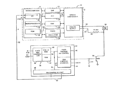
With reference to FIG. 1, a Texas Instruments TSP50CXX speech
synthesi?.ing chip 10, such as a TSP50ClX or TSP50C3X chip, includes an
LPC- 12 speech synthesizer circuit 12 (Linear Predictive Coding, 12 -pole
digital filter), which is capable of operating at a speech sample rate ranging
up to ten kilohertz or eight kilohertz (but typically at a data rate of only 1.5lcilobits per second for normal speech), and a microcomputer 14 capable of
executing up to 600,000 instructions per second. The microcomputer
includes an eight-bit microprocessor 16 with sixty-one instructions, a four-
l~ilobyte, siY-kilobyte, eight-kilobyte, sixteen-kilobyte, or thirty-two-lcilobyte
read-only memory 18 for storing program inslructions for microprocessor 16
and for storing speech data corresponding to about twelve, twenty, thirty,
sixty, or one hundred and twenty seconds of speech, and an input/output
circuit 20 for ten software-controllable input/output lines (in the case of a
TSP50C1X chip, seven lines for connecting the chip to an external memory
or an interface adapter for an external memory, as described below, and
three arbitrary lines). Speech synthesizing chip 10 also includes a random-
access memory 22 having a capacity of sixteen twelve-bit words and either
forty-eight or one hundred and twelve bytes of data, depending on the model
of the chip, an arithmetic lo,,ic unit 24, an internal timing circuit 26, for use
in conjunction with microcomputer 14 and speech synthesizer circuit 12,
and a speech address register (SAR) 13 for storing addresses at which
speech data is located.
CA 02250496 1998-09-23
WO 98/34215 PCT/US98/01699
In the case of a TSP50ClX chip, microcomputer 14 includes a
built-in interface that enables microcomputer 14 to connect directly to an
optional extemal Texas Instruments TSP60C18 or TSP60C8 1 read-only
memory that is designed to store speech data in addition to the speech data
stored in internal read-only memory 18 for use by speech synthesizer circuit
- 12 (a mode register in speech synthesizer chip 10 contains a nag indicating
whether data is to be retrieved from intemal read-only memory 18 or an
external memor~). This built-in interface includes input/output circuit 20
and seven of the input/output lines with which it is associated. The built-in
interface is controlled by the program in intemal read-only memory 18.
Referring to FIG. 2, as an altemative to connecting a TSP50ClX
speech synthesizing chip 10 directly to a TSP60C18 or TSP60C81 read-only
memory, speech synthesizing chip 10 can interface with an arbitrary,
industry-standard read-only memory 28 through an extemal Te~cas
Instruments TMS60C20-SE hardware interface chip 30. The connection
between speech synthesizing chip 10 and hardware interface chip 30
includes seven of the input/output lines of speech synthesizing chip 10, and
the connection between hardware interface chip 30 and read-only memory
28 includes about thirty-two lines. Thus, hardware interface chip 30 makes
it possible to connect speech synthesizing chip 10 to an e~ternal read-only
memory 28 having more output lines than could otherwise be connected to
speech synthesizing chip 10. Hardware interface chip 30 is controlled by
calls from the program in internal read-only memory 18.
The structure of the Texas Instruments TSPSOC3X chips is similar
to that of the TSP50ClX chips described above in connection with Figs. 1
and 2, except that the TSP50C3X chips do not include hardware for
connecting to and obtaining data from an external memory. An example of
code provided by Te~cas Instruments for progr~mming read-only memory 18
CA 02250496 1998-09-23
WO 98/34215 PCT/US98/01699
of a TSP50CXX speech synthesizing chip is attached to this application as
Text Appendix A.
With reference to FIG. 3, a Sunplus SPC40A, SPC256A, or
SPC512A audio synthesi~ing chip 34 contains a large microcontroller 36
that includes an eight-bit RISC controller 38, a 40, 256, or 512 kilobyte -
read-only-memory 40 for storing program instructions for RISC controller 38
and for storing audio data corresponding to about twelve seconds of sound,
and a 128-byte random-access memory 42 for use in conjunction with RISC
controller 38. Audio synthesizing chip 34 also includes an eight-bit digital-
to-analog converter 44 that functions as an audio synthesizer by converting
data from read-only-memory 40 to analog sign~l~ and an intemal timing
circuit 46 for coor-iina~in~ operation of microcontroller 36 and digital-to-
analog converter 44. A general input/output port 48 is provided for
connecting audio synthesizing chip 34 with e~ctemal memory for storing
additional audio data. Input/output port 48 has sixteen pins in the case of
an SPC40A chip, twenty-four pins in the case of an SPC256A chip, and
eleven pins in the case of an SPC512A chip.
Audio synthesizing chip 34 ~pically operates at a data rate of
about 24 kilobits per second, which is much higher than the typical data
sample rate of the speech synthesizing chip described above in connection
with FIG. 1. The speech synthesizing chip of FIG. 1 and the audio
synthesizing chip of FIG. 3 are of comparable price and both can store data
corresponding to about twelve seconds of sound. The audio synthesizing
chip of FIG. 3 must store more data than the speech synthesizing chip of
FIG. 1 because of the difference in the data sample rates, and thus it can be
said that the audio synthesizing chip of FIG. 3 uses a cheaper memory.
An e~amples of code provided by Sunplus for progr~mmin,~ the
read-only memory 40 of an SPC40A, SPC256A, or SPC512A audio
syntheci~ing chip is attached to this application as Text Appendix B.
CA 02250496 1998-09-23
WO 98/34215 PCT/US98tOl699
Refemng to Fig. 4, in a circuit according to the present invention
the input/output circuit 20 of a Texas Instruments TSP50C1X or TSP50C3X
speech synthesizing chip 10 is connected directly to the input/output port
48 of a SunplusSPC40A,SPC256A, or SPC512A audio synthe~i~in~ chip 34
by means of four input/output lines. The flow of audio data is illustrated by
paths 50, 52, and 54. In particular, speech synthesizer circuit 12 of speech
synthesi~in~ chip 10 receives speech data from read-only memory 18 of
speech synthesizing chip 10 along path 50 and also receives additional
speech data from read-only memory 40 of audio synthesizing chip 34 along
path 52. Digital-to-analog converter 44 of audio synthesizing chip 34 can
receive non-speech audio data (e.g., music, breaking glass, ringing bells)
from read-only memory 40 of audio synthesizing chip 34 along path 54.
Thus, speech synthesizer circuit 12 receives more speech data than can be
included in internal read-only memory 18, the additional speech data being
received from an external read-only memory 40 that is cheaper per unit of
speech data than internal read-only memory 18. Because digital-to-analog
converter 44 does not include the LPC speech processing capabilities of
speech synthesizer circuit 12, and because speech synthesizer circuit 12 is
not specifically designed for synthesizing non-speech sounds, it can be more
appropriate to direct non-speech data from read-only memory 40 to digital-
to-analog converter 4~ than speech synthesizer circuit 12. Both chips 10
and 3$ can create sound effects at the same time, with chip 10 producing
speech and chip 31 simultaneously producing non-speech sound effects~
The flow of data along paths 50 and 54 is conventional in each of
chips 10 and 34, but the flow of data along path 52 is obtained by
modifying the standard code for read-only memory 18 and the standard
code for read-only memory 40 to permit the direct connection between the
two chips. An example of a code modification for read-only memory 18 of
chip 10 is attached to this application as TeYt Appendix C and an example
CA 02250496 1998-09-23
WO 98134215 PCT/US98/01699
of a code modification for read-only memory 40 is attached as Text
Appendix D.
The modification of the code in read-only memory 40 instructs the
microprocessor of chip 34 to send speech data to input/output port 48
along path 52 rather than to digital-to-analog converter 44 along path 54.
The flow of data along path 52 between chips lO and 34 occurs through
four input/output lines of each of chips lO and 34. The four input/output
lines may be, for example, lines PA0, PAl, PA2, and PBl of chip 10, and
lines PD0, PD6, PDl, and PD4 respectively of chip 34.
The modification of the code in read-only memory 18 is a software
simulation of the hardware "LUAPS" and "GET" instructions of chip lO
(hardware instructions are implemented by hard-wired gates or micro-code
instructions progr~mmed into a chip during m~n1lf~ture~. With reference
to Fig. 5, ordinarily, a desired start address of a speech segment is loaded
into the A register of chip lO, and then the "LUAPS" instruction loads the
address from the A register into the SAR register (Speech Address Register)
on chip 10 and loads a parallel-to-serial register on chip 10 with the
contents of the address contained in the SAR register. Then, each
successive "GET X" instruction transfers X bits from the parallel-to-serial
register, to the A register of chip lO. The SAR register is incremented every
time the parallel-to-serial register is loaded, and whenever the parallel-to-
serial register becomes empty, it is loaded with contents of the address
contained in the SAR register. The groups of bits obtained by the "GET"
instructions form the fr~mes of LPC parameters described in detail in the
above-mentioned Te~as Instruments Design Manual and patents. In the
TSP50ClX chips, the address pointed to by the SAR register may be on-chip
or off-chip (if a specially configured Texas Instruments extemal memory is
used), because the TSP50ClX chips include hardware for connecting to and
ob~ining data from a speciallv configured Texas Instruments extemal
- 10 --
CA 02250496 1998-09-23
WO 98/34215 PCT/US98/01699
memory. In the TSPSOC3X chips the address pointed to by the SAR register
must be on-chip.
With reference to Fig. 6, according to the present invention, a
software simulation of the LUAPS and GET instructions of Fig. 5 is provided.
Instead of loading the address from the A register of the LPC chip into an
- SAR register as in the case of the LUAPS instruction of Fig. 5, CALL
STPNIR(X) causes pointer X to be stored in the ADPCM chip. Instead of
loading a parallel-to-serial register in the LPC chip with the contents of the
address contained in an SAR register and transferring bits from the parallel-
to-serial register to the A register of the LPC chip as in the case of the
LUAPS and GET instructions of Fig. 5, CALL PREPGET P(X) prepares the
ADPCM chip to send to the LPC chip the data to which pointer X points, and
CALL GET(Y) causes Y bits of data pointed to by pointer X to be read from
the ADPCM chip. In one embodiment, up to three pointers are used, so that
data can be read from up to three sets of storage locations corresponding to
three different sounds to be produced simultaneously by the LPC chip (for
example, music with three-part harmony).
With reference to Fig. 7, according to the input/output structure
of the LPC chip provided by the invention, the interface operation is
accomplished over four wires and is a command-driven structure. All
comm~nds are initialized on the side of the LPC chip and the ADPCM chip is
slave to the requested operations. Lines PAO-2 provide command codes to
the ADPCM chip, and line PBl indicates to the ADPCM chip that there is a
command on lines PAO-2. The LPC chip drops comm~ncl strobe line PBl
after setting up a command on lines PAO-2, and the ADPCM chip responds
by executing the command that was strobed. Thus, the processor of the
LPC chip initiates each command and the processor of the ADPCM chip
executes that command.
CA 02250496 1998-09-23
WO 98/34215 PCT/US98/01699
The various commAn(1s are shown in Fig. 8. Comm~nds 1-3
indicate that data pointer 1, 2, or 3 is to be sent to the ADPCM chip (this
corresponds to CALL STPNTR(X)), and comm~n-l~ 4-6 indicate that data to
which pointer 1, 2, or 3 points is to be read from the ADPCM chip (this
corresponds to CALL PREPGET P(X). In one particular embodiment useful
in certain toys, comms3n~ 0 instructs the ADPCM chip to strobe one of eight
strobe outputs to a game keyboard.
Referring again to Fig. 7, once the ADPCM chip has received the
a~o~iate command, line PA0 is used to read data from the ADPCM chip
or send a pointer to the ADPCM chip, and line PA1 is used to clock the data
serially into or out of the LPC chip. The ADPCM processor maintains
address pointers and counter that are advanced on clock events received on
line PA1. Line PA2 is used as a h~n-lsh~ke signal during the process of
reading data from the ADPCM chip.
With reference to Fig. 9, the LPC processor will perform CALL
STPNTR(X) by placing a 'Write Pointer X" comm~nd on lines PA0-PA2 and
lowering strobe line PB1. After a period of time sufficient for the ADPCM
chip to read the command has elapsed, the LPC chip provides the first bit of
data on line PA0 and then drops the clock signal on line PA1. During the
clock low time the ADPCM chip will accept and read in the bit on line PA0,
and then the next bit of data is placed on line PAl, and so on. Operations
that write data from the LPC processor to the ADPCM processor are done
without a han~h~kina signal. The data is clocked out by a fixed clock
cycle. The clock cycle time is the minimum time required for the ADPCM
chip to reliably clock in the data. The LPC processor completes the
operation by raising strobe line PB1 high.
When the ADPCM chip detects a 'Write Pointer X" comm~n-l it will
expect up to sixteen clocked data bits. When the operation is complete the
ADPCM chip stores the received value as Pointer X. It is possible to clock in
CA 02250496 1998-09-23
Wo 98/34215 PCT/US98/01699
fewer than sixteen bits of data to specify an address. In particular, the first
bit read out is the first bit of the address, and once strobe line PB1 goes
high, the unclocked data bits are all assumed to be zeros.
- The timing diagram of Fig. 9 is also used in connection with the"Write Keyboard Strobe" command ~Command 0 in Fig. 83. When the
ADPCM chip detects a "Write Keyboard Strobe" comm:ln~l it will expect a
clocked data bit to specify the next output state. Once strobe line PB1 goes
high, the ADPCM chip drives the strobe lines to the proper value. In this
way, the LPC chip controls eight outputs of the ADPCM chip, and thus the
interface bet~,veen the LPC and ADPCM chips effectively increases the
number of input/output lines available to the LPC chip.
With reference to Fig. 10, operations that read data from the
ADPCM chip to the LPC chip involve a h~n~lshA~cing signal on line PA2. The
"Read Data from Pointer X" commands (see discussion of Fig. 8 above)
require line PA2 to be high, which is necessary in order for hAn~l~hAkin~ to
proceed correctly. This is because line PA2isconfigured as an open-drain
output at initiAli~ation, externally pulled high by a 10K resistor.
When the LPC processor performs CALL PREPGET P(X) in order to
prepare to read data, the LPC chip issues a "Read Data from Pointer X"
command on lines PA0-1 and then lowers strobe PB1. In response to the
command, the ADPCM chip switches from its default input mode to an
output mode with respect to lines PA0 and PA2 of the LPC chip
(consequently, for a brief period of time, line PA0 of the LPC chip will receiveoutput -si~nAlc from both the LPC chip and the ADPCM chip). The ADPCM
chip then acknowledges acceptance of the command by pulling low line PA2
of the LPC chip. The LPC chip then performs CALL GET(Y) by setting line
PAO to an input, lowering line PAl to start the clocking of data, and raising
strobe line PB1 to indicate to the ADPCM chip that the LPC chip is ready to
receive data. The ADPCM chip places the first bit of data on line PAO and
CA 02250496 1998-09-23
WO 98/3421S PCT/US98/01699
releases line PA2. The LPC chip reads the data and raises the clock signal
on PA1 to signal that the data has been read. The ADPCM chip responds by
advz~n~in~ an intemal bit counter and pulling line PA2 low to acknowledge
receipt of the clock signal, and the LPC chip then responds by lowering line
PA1 to start the clocking of the next bit of data. The ADPCM chip then
places the next bit of data on line PA0 and releases line PA2, and the
process continues until the LPC chip has received as much data as it wants.
The LPC processor completes the operation by raising strobe line PB1 high
after Y bits of data have been received.
The four-wire interface between the two chips may also be used to
transfer non-speech data in either direction between the LPC RAM and the
ADPCM RAM, in a manner similar to the timing diagr~ms of Figs. 9 and 10,
in order to effectively e.Ypand the amount of RAM available to the master
chip (the LPC chip in the embodiments described above).
Fig. 11 is a flow chart of the operation of the ADPCM chip. The
ADPCM chip watches for strobe line PB1 of the LPC chip to go down ~step
100), and when this happens the ADPCM chip receives a read or write
command on lines PA0-PA2 of the ADPCM chip (step 102), handles the read
command (step 104; Fig. 10) or write command (step 106; Fig. 12), and then
returns to step 100.
In another alternative embodiment, the ADPCM chip can be set up
as the master microcontroller, and the LPC chip can function as the slave.
In this embodiment there is no need to perform a software simulation of the
LUAPS instruction of the LPC chip, because the pointers to the data in the
ADPCM chip all originate from the ADPCM chip itself. It will now be
apparent to those skilled in the art that data can be transferred from the
ADPCM chip to the LPC chip according to a technique similar to the
technique shown in the timing diagram of Fig. 10 (the initial synchronization
process at the be~innin~ of the timing diagram would differ but then the
-- 14 --
CA 02250496 1998-09-23
WO 98/34215 PCT/US98/01699
actual data transfer process could proceed in a marmer similar to that
shown in Fig. 10). Thus, a type of software simulation of the LUAPS and
GET instructions of the LPC chip can be performed, even though the LPC
chip in this particular embodiment functions as a slave.
With reference to Fig. 4, the outputs of speech synthesizer circuit
12 of chip 10 and digital-to-analog converter 44 of chip 34 are cormected to
a single speaker 56. The output of speech synthesizer circuit 12 is a pulse-
width-modulated push-pull bridge balanced drive for a 32-ohm speaker,
and the output of digital-to-analog converter 44, amplifled by transistor 58,
is a single-ended drive for an 8-ohm speaker. The output of digital-to-
analog converter 44, amplified by transistor 58, is connected to a node
between 16-ohm speaker 56 and 16-ohm resistor 60. Thus, the output of
digital-to-analog converter 44 is connected to two parallelly connected 16-
ohm resistances, or, in other words, an 8-ohm single-ended resistance. At
the same time, the output of speech synthesizer circuit 12 is connected to
two series-connected 16-ohm resistances, or, in other words, a 32-ohm
resistance.
When speech synthesizer 12 is silent, its push-pull bridge
balanced drive goes to low impedance, and the two outputs 62 and 64 of the
push-pull bridge balanced drive are at a positive voltage. This makes it
possible for current to pass from output 62, through speaker 56, and
through amplifier 58 while audio synthesizer integrated circuit chip 34 is
operating.
When chip 34 is silent, transistor 58 goes to high impedance (i.e.,
transistor 58 switches off). Meanwhile, pulse width modulated current may
pass between outputs 62 and 64 of the push-pull bridge balanced drive of
speech synthesizer 12 through speaker 56 while speech synthesizer 12 is
operating.
-- 15 --
CA 02250496 1998-09-23
W O 98/34215 PCTAUS98/01699
It is possible for both of chips 10 and 34 to operate
simultaneously with the single speaker 56 because, when chip 10 is
operating, output 62 of speech synthesizer 12 pulses high and low, and
whenever output 62 is high, current can pass from output 62 through
tr~nei.s~c-r 58 to produce the audio sounds synthe~i7ed by chip 34. The -
frequency of on and off pulsing of output 62 is too fast to a~fect the
perceived sound output produced by chip 34.
There has been described novel and improved apparatus and
techniques for speech and sound synthesizing. It is evident that those
skilled in the art may now make numerous uses and modifications of and
departures from the specific embodiment described herein without
departing from the inventive concept.
- 16 -
CA 02250496 1998-09-23
W O9813421S PCTAUS98/01699
APPENDIX A
Title: SPEECH AND SOUND SYNTHESIZNG
Applicant: Hasbro, Inc.
S~ lJTE SHEET (RULE 2~)
CA 02250496 1998-09-23
W O 98/34215 PCTrUS98/01699
* Standard TI D6 Speech Engine
,~A~AAAAAAAAAAAAAAAAA~AAAAAAAAAAAAAAAAAAI.AA~A~AAAAA~AAAAAAA
* Speak Utterance - Phrase number in A register
AAAAAAAAA~AAAAAAAAAAAAAAAAAAAAAAAAAA~AA~AAAAAAAAAAAAAAAAA
SPEAK INTGR
BR SPEAK3 -Go to getl st word number
*
SPEAKl RETN -yes, exit routine
SPEAK3 SALA -Double inde~ to get offset
ACAAC SPEECH -Add base of table
LUAB -get address MSB
LAC
LUAA -Get address LSB
XBA
SALA4 -Combine MSB and LSB
SALA4
ABAAC
LUAPS -Load Speech Address Register
CLA -Kill Kll and K12 pararneters
TAMD Kl 1
TAMD K12
TAMD FLAGS -Init flags for speech
CLA -Load C2 parameter
ACAAC C2_Value
TAMD C2
CLA -Load Cl parameler
ACAAC C l_Value
TAMD C 1
* * * * *
* Now we give an initial value to the Pitch in case the utterance starts
* with a silent frarne.
* * * * *
ACAAC #OC
TAMD PHV 1
TAMD PHV2
* * * * *
* Now we preload the first two frarnes.
* * * * *
CALL UPDATE -Load first frarne
CALL UPDATE -Load 2nd frarne
* * * * *
18
SUBSTITUTE SHEET (RULE 26
CA 02250496 1998-09-23
W O 98/34215 ' PCTrUSg8/01699
* Now we give some values to the Timer and Prescaler so that we
can do a
* valid interpolation on the first call to INTP. Then I do the first
* call to INTP to preload the first valid interpolation.
* * * * *
TCA PSVALue -Initialize prescale
TAPSC
TCA #7F -Pretend there was a previous update
TAMD TIMER
TCA #FF -Set timer to max value to
TATM -.. disable interpolation
CALL INTP -Do first interpolation
* * * * *
* Now we enable the synthesizer for speech
*****
TCX MODE -Turn on LPC synthesizer
ORCM LPC_ON
TMA
TAMODE
RETI -Reset interrupt pending latch
ORCM INT_ON -Enable interrupt
TMA
TAMODE
*****
Now we loop until the utterance is complete. When the utterance is
* finished, the rouline UPDATE will execute a RETN instruction which
* will exit this roucine. In the mean time, this loop will poll the
* Timer register and update the ~rame whenever it underflows.
* * * * *
SPEAK_LP TCX FLAGS
TSTCM Update_Flg -Update already done?
BR SPEAK_LP -yes, loop
TCX TIMER -Get old timer
TMA register valu
TAB -into B register
TTMA -Get new timer register
SARA -value and scale it.
TAM -Store new value
XBA -Exchange new and old values
SBAAN -Subtract new from old
BR UPDATE-If underflowed, do an update
TMA -Get new timer value again.
ANEC 0-Is it about to underflow?
BR SPEAK_LP no, loop again
19
SIJ~ JTE SHEET (RULE 26)
CA 02250496 1998-09-23
WO 98/34215 PCT/US98/01699
BR UPDATE yes, do update now
*****
* INTERPOLATION ROUTINE
* ~ * * *
* First we need to get the current value of the timer register and store
* it away. It will be divided by two with the SARA instruction so that
* the most significant bit is guaranteed to be zero so that it will always
* be interpreted as a positive number during the interpolation.
*****
INTP TTMA -Get timer register contents
SARA -shift to make positive
TAMD SCALE -and store it
*****
* Nex~ we need to see if the frarne type has changed between voiced
and
* unvoiced frames. If it has, we do not want to inteIpolale between
* them; we just want to use the current frame values until we have
two
* frarnes of the sarne type to interpolate between.
*****
TCX FLAGS -Test to see if Interpolation
TSTCM Int_Inh -is inhibited
BR NOINT -yes, use inhibit code
BR INTPCH -yes, use inhibit code
*****
* The following code is reached if interpolation is inhibited. It
sets
* the stored tirner value to #7F which effectively forces the
interpolation
* to yield the old values for the working values, thus effectivelv
disabling
* interpolation.
* * * * ~
NOINT TCA #7F -Set Scale factor to
TAMD SCALE -highest value
* If the new frame has a voicing different fromthe last fr~rrle,
* we want to zero the ener~ until the Unvoiced bit in the mode
* register is changed and the K paramaters are all to the current
* values. We therefore check in this section of code to see if
* the frame voicing is different from the setting in MODE. If it
* is, we zero the energy until after MODE is modified.
*
TCX FLAGS
TSTCM Unv_Flg2 -Is new frame unvoiced?
SUBSTITUTE SHEET (RULE 26)
CA 02250496 1998-09-23
PCT/US9810109
WO 98/3421~
-
BR Uv -Yes, go to unvoiced branch
TCX MODE -New fr~me is voiced
TSTCM UNV -Has mode been changed to voiced?
BR ClrEN -No, clear the energy
Uv TCX MODE -New frame is unvoiced
TSTCM UNV -Has mode been changed to unvoiced?
BR INTPCH -Yes, no action required
ClrEN CLA -Zero Energy during update
TAMD EN
BR INTPCH
* * * * *
* Interpolate Pitch and store the result in the working register
* * * * *
INTPCH INTGR -Need Integermode for pitch
TCX PHV2 -Combine pitch and fractional
TMAIX -pitch and leave in
SALA4 -the B register
AMAAC
LXC
TAB
TMAIX -Combine current pitch and
SALA4 -current fractional pitch
AMAAC -and leave in A register
SBAAN -(Pcurrent- Pnew)
TCX SCALE
AXMA -(Pcurrent - Pnew) * Timer
ABAAC -Pnew + (Pcurrent - Pnew)* Timer
SALA -LSB must be 0 to address e~citation table
TASYN -Write to pitch register
EXTSG -Allow negative K parameters
* * * * *
* Interpolate Energy and store the result in the working register
* * * * *
TCX ENV2 -Combine energy and fractional
TMAIX -energy and leave in
SALA4 -the B register
AMAAC
IXC
TAB
TMAIX -Combine current ener~y and
SALA4 -current fractional ener~y &
AMAAC -leave in A register
21
SUBSTITUTE SHEET (RULE 26)
CA 02250496 1998-09-23
WO 98/34215 PCT/US98/01699
SBAAN -(Ecurrent- Enew)
TCX SCALE
AXMA -(Ecurrent - Enew) * Timer
ABAAC -Enew + (Ecurrent - Enew) * Timer
* TAMD EN_TEMP -Store Energy til mode is Swil:ched
TAMD EN
*
EXTSG -Allow K pararneters to be negative
*****
* Interpolate Kl and store the result inthe working Kl register
* * * * *
TCX KlV2 -Combine New Kl and New
TMAIX -fractional Kl and
SALA4 -leave in the B register
AMAAC
LYC
TAB
TMAIX -Combine current Kl and
SALA4 -current fractional Kl and
AMAAC -leave in the A register
SBAAN -(Klcurrent- Klnew)
TCX SCALE
AXMA -(Kl current - Klnew) * Timer
ABAAC -Klnew+(Kl current-Klnew) * Timer
TAMD Kl -~oad interpolated value to synth
* * * * *
* Interpolate K2 and store the result in the working K2 ret"ster
* * * * *
TCX K2V2 -Combine New K2 and New
TMAIX -fractional K2 and
SALA4 -leave in the B register
AMAAC
IXC
TAB
TMAIX -Combine current K2 and
SALA4 -current fractional K2 and
AMAAC -leave in the A register
SBAAN -(K2current- K2new)
TCX SCALE
AXMA -(K2current - K2new) * Timer
ABAAC -K2new+(K2current-K2new) * Timer
TAMD K2 -Load interpolated value to synth
* * * * *
* Interpolate K3 and store the result in the working K3 register
* * * * *
TCX K3V2 -Combine New K3 and New
22
SUBSTITUTE SHEET (RULE 26)
CA 02250496 1998-09-23
W O 98/34215 PCTrU$98/016g9
TMAIX -fractional K3 and
SALA4 -leave in the B register
TAB
TMAIX -Combine current K3 and
SALA4 -current fractional K3 and
SBAAN -(K3current - K3new)
TCX SCALE
AXMA -(K3current - K3new) * Tirner
ABAAC -K3new+(K3current-K3new) * Timer
TAMD K3 -Load interpolated value to synth
*****
* Interpolate K4 and store the result in the working K4 register
* * ~ * *
TCX K4V2 -Combine New K4 and New
TMAIX -fractional K4 and
SALA4 -leave in the B register
TAB
TMAIX -Combine current K4 and
SALA4 -current fractional K4 and
SBAAN -(K4current- K4new)
TCX SCALE
AXMA -(K4current - K4new) * Timer
ABAAC -K4new+(K4current-K4new) * Timer
TAMD K4 -Load interpolated value to synth
* * * * *
* Interpolate K5 and store the result in the working K5 register
* * * * *
TCX K5V2 -Put New K5 (adjusted to
TMAIX -12 bits) in B register
SALA4
TAB
TMAIX -Put Current K5 (adjusted to
SALA4 -12 bits) in A register
SBAAN -(K5current- K5new)
TCX SCALE
AXMA -(K5curren~ - K5new) * Timer
ABMC -K5new+(K5current-K5new) * Timer
TAMD K5 -Load interpolated value to synth
* * * * *
* Interpolate K6 and store the result in the working K6 register
* * * * *
TCX K6V2 -Put New K6 (adjusted to
TMAIX -12 bits) in B register
SALA4
TAB
TMAIX -Put Current K6 (adjusted to
SALA4 -12 bits) in A register
23
SU~S 111 ~)TE SHEET (RULE 26)
CA 02250496 1998-09-23
W 0 98/34215 rCTrUS98/01699
SBAAN -(K6current- K6new)
TCX SCALE
AXMA -(K6current - K6new) * Tirner
ABAAC -K6new+(K6current-K6new) * Timer
TAMD K6 -Load interpolated value to synth
* * * * *
* Interpolate K7 and store the result in the working K7 register
* * * * *
TCX K7V2 -Put New K7 (adjusted to
TMAIX -12 bits) in B register
SALA4
TAB
TMAIX -Put Current K7 (adjusted to
SALA4 -12 bits) in A register
SBAAN -(K7current- K7new)
TCX SCALE
AXMA -(K7current - K7new) * Timer
ABAAC -K7new+(K7current-K7new) * Timer
TAMD K7 -Load interpolated value to synth
* * * * *
* Interpolate K8 and store the result in the working K8 register
* * * * *
TCX K8V2 -Put New K8 (adjusted to
TMAIX -12 bits) in B register
SALA4
TAB
TMAIX -Put Current K8 (adjusted to
SALA4 -12 bits) in A register
SBAAN -(K8current - K8new)
TCX SCALE
AXMA -(K8current - K8new) * Timer
ABAAC -K8new+(K8current-K8new) * Timer
TAMD K8 -Load interpolated value to synth
* * * * *
* Interpolate K9 and store the result in the working K9 register
* * * * *
TCX K9V2 -Put New K9 (adjusted to
TMAIX -12 bits) in B register
SALA4
TAB
TMAIX -Put Current K9 (adjusted to
SALA4 -12 bits) in A register
SBAAN -(K9current- K9new)
TCX SCALE
AXMA -(K9current - K9new) ~ Timer
ABAAC -K9new+(K9current-K9new) * Timer
TAMD K9 -Load interpolated value to synth
2~
SU~:I l 11 UTE SHEET (RULE 25)
CA 02250496 1998-09-23
WO 98/342l5 PCT/US98/01699
~ * ~ * *
* Interpolate K10 and store the result in the working K10 register
f * * * *
TCX KlOV2 -Put New K10 (adjusted to
TMAIX -12 bits) in B register
SALA4
TAB
TMAIX -Put Current K10 (adjusted to
SALA4 -12 bits) in A register
SBAAN -(KlOcurrent- KlOnew)
TCX SCAI,E
AXMA -(KlOcurrent - KlOnew) * Timer
ABAAC -KlOnew+(KlOcurrent-KlOnew) * Timer
TAMD K10 -Load interpolated value to synth
* * * * *
* Kl 1 and K12 are not needed for LPC 10, so I have taken them out.
* * * * *
* * * * *
* Set voiced/unvoiced mode according to current frame type.
This is
* done in a two step fashion: first the value in the MODE register
* is adjusted with an AND or OR operation, then the result is
written
* to the synthesizer with a TAMODE operation. We do it this way
to keep
* a copy of the current status of the synthesizer mode at all
time.
* * * * *
STMODE INTGR -Back to integer mode
TCX FLAGS
ANDCM -Update_Flg -Signal that interp done
TSTCM Unv_Flg2 -Is current frame unvoiced?
BR SETW -Yes, set mode to unvoiced
TCX MODE -No, set mode to voiced
ANDCM ~LPC_UNV
TMA
TAMODE
*
TMAD EN_TEMP -Change Energy parameter
* TAMD EN -.. to correctvalue
*
RETI-Return from interrupt
RETN-Retum from first call
SETW TCX MODE-Current frame is unvoiced, so
ORCMLPC_UNV-Set mode to unvoiced.
- TMA
TAMODE
~5
SUBSTITUTE SHEET (RULE 26)
CA 02250496 1998-09-23
WO 98/34215 PCTtUS98/01699
* TMAD EN_TEMP -Change Energy parameter
* TAMD EN -.. to correctvalue.
*
RETI -Return from interrupt
REIN -Return from first call
* * ~ * ~
* Update the parameters for a new frame
* * * * *
* First we inhibit the operation of the interpolation routine.
* * * * *
UPDATE TCX MODE
ANDCM -INT_ON
TMA
TAMODE
* * * * *
* To prevent double updates, if the stored value of the timer register
* is zero, then we need to change it to #7F. If we do not do this, than
* the polling routine will discover an under~low and call Update a
second
* ti--le.
* * * * *
TCX TIMER -Get stored value
TMA -of Timer into A
ANEC 0 -Is it zero?
BR UPDT00 -no, do nothing
TCA #7F -yes, replace value
TAM
* * * * *
* First we need to test to see if a stop frame was encountered on the
last
* pass through the routine. If the previous frame was a stop frame,
-e
* need to turn off the synthesizer and stop speaking.
* * * * *
UPDT00 TCX FLAGS
TSTCM STOPFLAG -Was stop frame encountered
BR STOP -yes, stop speaking
* Transfer the state of the previous frame to the Unvoiced flag
(Current)
* and set the mode mirror buffer to reflect the voicing of the previous
frame.
TSTCM Unv_Flgl -Was previous frame unvoiced?
BR SUNVL -Yes, set current frame unvoiced
ANDCM #7F -No, set current frame voiced
26
SlJts~ 111 ~JTE SHEET (RULE 26)
CA 02250496 1998-09-23
WO 98/34215 PCT/US98/01699
BR TSIL
SUNVL ORCM Unv_Flg2 -Set current frame unvoiced.
* * * * *
* Transfer the state of ~e previous frame to the Silence flag ICurrent)
* and set the mode mirror buffer
* * * * *
TSIL TSTCM Sil_Flgl -Was previous fr~m e silent?
BR SSIL -Yes, set current frame silen
ANDCM -Sil_Flg2 -No, set current frame not silent
BR ZROFLG
SSIL ORCM Sil_Flg2 -Set current fr~rne unvoiced.
* * * * *
* Reset the Repeat Flag, Silence Flag, Unvoiced Flag, and
Interpolation
* Inhibit flag so that new values can be loaded in this routine.
* * * * *
ZROFLG TCX FLAGS
ANDCM #C5
* * * * *
* Transfer the current new frame parameters into the storage location
used
* for the current frame parameters.
* * * * *
TCX ENV2-Transfer new frame ener~y
TMAIX-to current frame location
TAMD ENVl
TMAIX-Transfer new fractional ener~y
LXC-to current frame location
TAMIX
*-----PITCH-----
TMAIX-Transfer new frarne pitch
TAMD PHV 1-to current fr~ m e location
TMAIX -Transfer new fractional pitch
IXC -to current frame location
TAMIX
*-----Kl-----
TMAIX -Transfer new frame Kl paramete
TAMD KlVl-to current frarne location
TMAIX -Transfer new fractional Kl par
IXC -to current frame location
TAMIX
*-----K2-----
TMAIX -Transfer new frame K2 paramete
TAMD K2V 1-to current frarne location
TMAIX -Transfer new fractional parame
IXC -to current frarne location
TAMIX
2~
SUBSTITUTE SHEET (RULE 26)
CA 02250496 1998-09-23
WO 98/34215 PCTtUS98/01699
*-----K3-----
TMAIX -Transfer new frame K3 pararnete
TAMIX
*-----K4-----
TMAIX -Transfer new frame K 4 paramete
TAMIX
*----- K 5-----
TMAIX -Transfer new frame K ~ paramete
TAMIX -to current frame location
*-----K 6-----
TMAIX -Transfer new frame K 6 paramete
TAMIX -to current frame location
*----- K 7-----
TMAIX -Transfer new frame K 7 paramete
TAMIX -to current frame location
*-----K 8-----
TMAIX -Transfer new frame K 8 paramete
TAMIX -to current frame location
*-----K 9-----
TMAIX -Transfer new frame K9 paramete
TAMIX -to current frame location
*-----K 1 O-----
TMAIX -Transfer new frame K 10 paramet
TAMIX -to current frame location
* * * * *
* K l l and K12 are not used in LPC 10 synthesis, so the code has
been
* commented out.
* * * * *
*-----K 1 1-----
* TMAIX -Transfer new frame K11 par~met
* TAMIX -to current frame location
*-----K12-----
* TMAIX -Transfer new frame K12 paramet
* TAMIX -to current frame location
* * * * *
* We have now discarded the "current" values by replacing it with
the
* "new" values. We now need to read in another fr~me of
speech data and
* used them as the new "new" values.
* * * * *
*--- --ENERGY -----
CLA
TCX FLAGS
GET EBITS -Get coded energy
28
SU~ JTE SHEET (RULE 26)
CA 02250496 1998-09-23
WO 98/34215 PCT/US98/01699
ANEC ESILENCE -Is it a silent frame?
BR UPDT0 -No, continue
ORCM Sil_Flgl+Int_Inh -Yes, set silence flag
BR ZeroKs -zero K params
UPDT0 ANFC ESTOP -Is it a stop frame?
BR UPDTl -No, continue
ORCM STOPFLAG+Sil_Flgl+Int_Inh yes, set flags
BR ZeroKs -Zero Ks
UPDTl ACAAC TBLEN -Add table offset to energy index
LUAA -Get decoded energy
TAMD ENV2 -Store the Energy in RAM
* * * * *
* If this is a silent frame, we are done with the update If the previous
* frame was silent, the new fr~me should be spoken immediately with
no
* ramp up due to in~erpolation.
* * * * *
TCX FLAGS
TSTCM Sil_Flgl -Is this a silent frame?
BR RTN -yes, exit
* * * * *
* A repeat frame ~,vill use the K pararneter from the previous frame. If
it
* is, we need to set a flag.
* * * * *
UPDT2 GET RBITS -Get the Repeat bit
TSTCA #01 -Is this a repeat frame?
BR SFLGl -yes, set repeat flag
BR UPDT3
SFLG 1 ORCM R_FLAG -Set repeat flag
*-----PITCH-----
UPDT3 CLA
GET 4 -Get coded pitch
GEr 3 -Get coded pitch
ANEC PUnVoiced -Is the frame unvoiced?
BR UPDT3A -no, continue
ORCM Unv_Flgl -yes, set unvoiced flag
UPDT3A SALA -Double coded pitch and
ACAAC TBLPH -add table offset to point to table
LUAB -Get decoded pitch
IAC
LUAA -Get decoded fractional pitch
- TCX PHV2 -Store the pitch and ~ractional
TBM -pitch in RAM
29
SUBSTITUTE SHEET (RULE 26)
CA 02250496 1998-09-23
WO 98/3421S PCT/US98/0l699
IXC
TAM
* * * * *
* If the voicing has changed with the new frame, then we need to
change
* the voicing in the mode register.
* * * * *
TCX FLAGS
TSTCM Unv_Flgl -Is the new frame unvoiced?
BR UPDT3B -yes, continue
BR VOICE -no, go to voiced code
* * * * *
* The following code is reached if the new frame is unvoiced. We
inspect
* the flags to see if the previous frame was either silent or voiced.
* If either condition applies, then we branch to code which inhibits
* interpolation.
* * * * *
UPDT3B TSTCM Sil_Flg2 -Was the previous frame silent?
BR UPDT5 -yes, inhibit interpolation
TSTCM Unv_Flg2 -Was the previous frame unvoiced
BR UPDT4 -yes, no need to change anything
BR UPDT5 -no, inhibit interpolation
* * * * *
* The following code is reached if the new frame is voiced. We
inspect the
* flags to see if the previous frame was also voiced. If it was not, we
* need to inhibit interpolation.
VOICE TSTCM Unv_Flg2 -Was the previous frame voiced?
BR UPDT5 -no, set no interpolation flag
BR UPDT4 -yes, no need to change anvthing
UPDT~ ORCM Int_Inh -Inhibit interpolation
* * * * *
* Now we test the repeat flag. If the new frame is a repeat frame, then
* the current values are used for the K factors, so new values do not
need
* to be loaded and we can exit the routine now.
* * * * ~
UPDT~ TSTCM R_FLAG -Is repeat flag set?
BR RTN -yes, exit routine
* * * * *
* Now we need to load the "new" K factors (K1 through K10).
Each K
* factor is a 12 bit value which will be stored in ~wo bytes. The most
SUBSTITUTE SHEET (RULE 26)
CA 02250496 1998-09-23
WO 98134215 PCT/US98/01699
* ~i~nific:~nt 8 bit in the first byte, and the least signif~cant 4 bits
* (called the fractional value) in the second byte. For K5 throu~h
K12,
* the fractional part is assumed to be zero. Kl 1 and K12 ~e not used
in
*LPC synthesis, and the code loading them is commented out. A
coded
* factor is read into the A register. It is then converted to a ~ Lnter
* to a table element which contains the uncoded factorO Since
each table
* element consists of two bytes, the conversion consists of doubling
the
* uncoded factor and adding the offset of the start of the table.
The
* uncoded factor is fetched and stored into RAM.
* ~ * * *
*~ Kl-----
CLA
GET 4 -Get coded Kl
GET 2 -Get coded Kl
SALA -Convert it to a
ACAAC TBLKl pointer to table element
LUAB -Fetch MSB of uncoded Kl
IAC
LUAA -Fetch fractional Kl
TCX KlV2
TBM -Store uncoded Kl
IXC
TAM -Store fractional Kl
*-----K2-----
CLA
GET 4 -Get coded K2
G~;T 2 - Get coded K2
SALA -Convert it to a
ACAAC TBLK2 pointer to table element
LUAB -Fetch MSB of uncoded K2
IAC
LUAA -Fetch fractional K2
TCX K2V2
TBM -Store uncoded K2
IXC
TAM -Store fractional K2
*-----K3-----
CLA
GEI 4 -Get Inde.Y into K3 table
31
SUBST1TUTE SHEET (RULE 26)
CA 02250496 1998-09-23
WO 98/34215 PCT/US98/01699
GET 1 -Get Index into K3 table
ACAAC TBLK3 -and add offset of table to it
LUAA -Get uncoded K3
TAMD K3V2 -and store it in RAM
*-----K4-----
CLA
GET 4 -Get Index into K~ table
GET 1 -Get Index into K4 table
ACAAC TBLK4 -and add offset of table to it
LUAA -Get uncoded K4
TAMD K4V2 -and store it in RAM
~ * * ~ *
* If this is a unvoiced frame, we only use four K factors, so we load
* zeroes to the rest of the K factors. If this is a voiced frame, load
* the rest of the uncoded factors.
TCX FLAGS
TSTCM Unv_Flgl -Is this an unvoiced frame?
BR UNVC -Yes, zero rest of factors
* * * * *
* The following code is executed if the current fr~me is voiced. Since
* we assume that the fractional parameter is zero for the r~m~inin~, K
* factors, the table elements are only one byte long. The conversion to
a
* table pointer now consists of adding the offset of the start of the
table.
* * * ~ *
*-----K5-----
CLA
GET K5BITS -Get Index into K5 table
ACAAC TBLK;: -and add offset of table to it
LUAA -Get uncoded K~
TAMD K5V2-and store it in RAM
*-----K6-----
CLA
GET K6BITS-Get Index into K6 table
ACAAC TBLK6 -and add offset of table to i
LUAA -Get uncoded K6
TAMD K6V2-and store it in RAM
*-----K7-----
CLA
GET K7BITS-Get Index into K7 table
ACAAC TBLK7 -and add offset of table to i
LUAA -Get uncoded K7
TAMD K7V2-and store it in RAM
* ----K8-----
32
SUBSTITUTE SHEET (RULL 26)
CA 02250496 1998-09-23
WO 98/34215 PCT/US98/01699
CLA
GET K8BITS -Get Index into K8 table
ACAAC TBLK8 -and add offset of table to i
LUAA -Get uncoded K8
TAMD K8V2 -and store it in RAM
*-----K9-----
CLA
GET K9BITS -Get Index into K9 table
ACAAC TBLK9 -and add offset of table to i
LUAA -Get uncoded K9
TAMD K9V2 -arld store it in RAM
*-----K10-----
CLA
GET KlOBITS -Get Index into K10 table
ACAAC TBLK10 -and add offset of table to i
LUAA -Get uncoded K10
TAMD KlOV2 -and store it in RAM
* * * * *
* Since Kl 1 and K12 are not used in LPC10, the Kl 1 and K12 code is
removed
* * * ~ *
BR RTN
* * * ~ *
* The following code is executed if the K par~meters need to be
cleared.
* If the new frarne is a stop frame or a silent frame, we clear all K
* parameters and set ener~ to zero. If the new frame is an unvoiced
* fr~rne, then we need to zero out the unused upper K parameters.
~ ~ ~ ~ *
ZeroKs CLA
TAMD ENV2 -Kill Ener~
TAMD ENV2 + 1
TAMD KlV2 -Kill Kl
TAMD KlV2+1
TAMD K2V2 -Kill K2
TAMD K2V2 + 1
TAMD K3V2 -Kill K3
TAMD K4V2 -Kill K4
UNVC CLA
TAMD K5V2 -Kill K5
TAMD K6V2 -Kill K6
TAMD K7V2 -Kill K7
- TAMD K8V2 -Kill K8
TAMD K9V2 -Kill K9
TAMD KlOV2 -Kill K10
- BR RTN
* * * * *
33
SUBSTITUTE SHEET (RULE 26)
CA 02250496 1998-09-23
WO 98/34215 PCT/US98/01699
* STOP AND RETURN
* * * * *
* The following code has three entry points. STOP is reached if the
* current frame is a stop flag, it turns off synthesis and returns to
* the program. RTN is the general exit point for the UPDATE routine,
* it sets the Update flag and leaves the routine.
* * * * *
STOP TCX MODE
ANDCM ~LPC -Turn off synthesis
ANDCM ~ENA1 -Disable interrupt
ANDCM ~UNV -Go back to voiced for next word
ORCM PCM -Enable PCM mode
TMA
TAMODE -Set mode per above setting
CLA
TASYN -Write a zero to the DAC
TCA #FA
BACK IAC -Wait for 30 instluction cycles
BR OUT
BR BACK
OUT TCX MODE -Disable PCM
ANDCM -PCM
TMA
TAMODE -Set mode per above setting
BR SPEAKl -Go back for next word
RTN TCX FLAGS -Set a flag indicating that
ORCM Update_Flg -the parameters have been
updated
TCX MODE -Get mode
TSTCM LPC-Are we speaking yet?
BR RTN1-Yes, reenable interrupt
RETN-No, return for mode data
*
RTN 1 ORCM ENAl -Reenable the interrupt
TMA
TAMODE
BR SPEAK_LP -Go back to loop
unl
* * ~ * *
* D6 (654P74) SPEECH DECODING TABLES
* * * * *
* ENERGY DECODING TABLE
* * * * *
SUBSTITUTE SHEET (RULE 26)
CA 02250496 1998-09-23
W O 98/34215 PCTrUS98/01699
TBLEN BYTE #00,#01,#02,#03,#04,#05,#07,#0B
BYTE #ll,#lA,#29,#3F,#55,#70,#7F,#OO
* * * ~ *
*D6PITCH DECODING TABLE
* * * * *
TBLPH BYTE #OC,#OO
BYTE #10,#00
BYTE #10,#04
BYTE #10,#08
BYTE #11,#00
BYTE #11,#04
BYTE #11,#08
BYTE #ll,#OC
BYTE #12,#04
BYTE #12,#08
BYTE #12,#OC
BYTE #13,#04
BYTE #13,#08
BYTE #14,#00
BYTE #14,#04
BYTE #14,#0C
BYTE #15,#00
BYTE #15,#08
BYTE #15,#0C
BYTE #16,#04
BYTE #16,#0C
BYTE #17,#00
BYTE #17,#08
BYTE #18,#00
BYTE #18,#04
BYTE #18,#0C
BYTE #19,#04
BYTE #l9,#OC
BYTE #lA,#04
BYTE #lA,#OC
BYTE #lB,#04
BYTE #lB,#OC
BYTE #lC,#04
BYTE #lC,#OC
BYTE #lD,#04
BYTE #lD,#OC
BYTE #lE,#04
- BYTE #lF,#OO
BYTE #lF,#08
BYTE #20,#00
BYTE #20,#0C
BYTE #21,#04
3j
SUBSTITUTE SHEET (RULE 26)
CA 022~0496 1998-09-23
PCT~S98/01699
W098/34215
BYTE #21,#0C
BYTE #22,#08
BYTE #23,#00
BYTE #23,#0C
BYTE #24,#08
BYTE #25,#00
BYTE #25,#0C
BYTE #26,#08
BYTE #27,#04
BYTE #28,#00
BYTE #28,#0C
BYTE #29,#08
BYTE #2A,#04
BYTE #2B,#OO
BYTE #2B,#OC
BYTE #2C,#08
BYTE #2D,#04
BYTE #2E,#04
BYTE #2F,#OO
BYTE #30,#00
BYTE #30,#0C
BYTE #31,#OC
BYTE #32,#08
BYTE #33,#08
BYTE #34,#08
BYTE #35,#08
BYTE #36,#08
BYTE #37,#08
BYTE #38,#08
BYTE #39,#08
BYTE #3A,#08
BYTE #3B,#OC
BYTE #3C,#OC
BYTE #3D,#OC
BYTE #3F,#OO
BYTE #40,#04
BYTE #41,#04
BYTE #42,#08
BYTE #43,#0C
BYTE #45,#00
BYTE #46,#04
BYTE #47,#08
BYTE #49,#00
BYTE #4A,#04
BYTE #4B,#OC
BYTE #4D,#OO
BYTE #4E,#08
36
SUBSTITUTE SHEET(RULE26
CA 02250496 1998-09-23
PCT~S98/01699
W098/34215
BYTE #50,#00
BYTE #51,#04
BYTE #52,#0C
BYTE #54,#08
BYTE #56,#00
BYTE #57,#08
BYTE #59,#04
BYTE #5A,#OC
BYTE #5C,#08
BYTE #5E,#04
BYTE #60,#00
BYTE #61,#OC
BYTE #63,#08
BYTE #65,#04
BYTE #67,#04
BYTE #69,#00
BYTE #6B,#OO
BYTE #6D,#OO
BYTE #6F,#OO
BYTE #71,#00
BYTE #73,#04
BYTE #75,#04
BYTE #77,#08
BYTE #79,#0C
BYTE #7C,#OO
BYTE #7E,#04
BYTE #80,#08
BYTE #82,#0C
BYTE #85,#04
BYTE #87,#0C
BYTE #8A,#04
BYTE #8C,#OC
BYTE #8F,#08
BYTE #92,#00
BYTE #94,#0C
BYTE #97,#08
BYTE #9A,#04
BYTE #9D,#OO
BYTE #AO,#OO
* * * * *
*Kl DECODING TABLE
* * * * *
TBLKl BYTE #81,#00
BYTE #82,#04
BYTE #83,#04
BYTE #84,#08
BYTE #85,#0C
37
SUBSTITUTE SHEETtRULE26
CA 022~0496 1998-09-23
WO g8/34215 PCT/US98/01699
BYTE #87,#00
BYTE #88,#04
BYTE #89,#0C
BYTE #8B,#04
BYTE #8C,#OC
BYTE #8E,#04
BYTE #90,#00
BYTE #91,#OC
BYTE #93,#08
BYTE #g5,#08
BYTE #97,#04
BYTE #99,#08
BYTE #9B,#08
BYTE #9D,#08
BYTE #9F,#OC
BYTE #A2,#00
BYTE #A4,#04
BYTE #A6,#0C
BYTE #A9,#04
BYTE #AB,~08
BYTE #AE,#OO
BYTE #BO,#OC
BYTE #B3,#08
BYTE #B6,#04
BYTE #B9,#00
BYTE #BC,#OO
BYTE #BF,#04
BYTE #C2,#04
BYTE #C5,#08
BYTE #C8,#0C
BYTE #CC,#04
BYTE #CF,#OC
BYTE #D3,#08
BYTE #D7,#08
BYTE #DB,#04
BYTE #DF,#04
BYTE #E3,#08
BYTE #E7,#0C
BYTE #EC,#OO
BYTE #FO,#04
BYTE #F4,#0C
BYTE #F9,#OC
BYTE #FE,#OC
BYTE #04,#04
BYTE #O9,#OC
BYTE #OF,#04
BYTE #15,#08
38
SUBSTITUTESHEET(RULE26)
CA 02250496 1998-09-23
W098/34215 PCT~S98/01699
BYTE #lC,#08
BYTE #23,#08
BYTE #2A,#OC
BYTE #32,#08
BYTE #3A,#08
BYTE #42,#0C
BYTE #4B,#08
BYTE #54,#00
BYTE #SC,#04
BYTE #65,#00
BYTE #6E,#OO
BYTE #78,#08
* K2 DECODING TABLE
TBLK2 BYTE #8A,#OO
BYTE #98,#00
BYTE #A3 ,#OC
BYTE #AD,#OC
BYTE #B4,#08
BYTE #BA,#08
BYTE #CO,#OO
BYTE #C5,#00
BYTE #C9,#OC
BYTE #CE,#04
BYTE #D2,#0C
BYTE #D6,#0C
BYTE #DA,#OC
BYTE #DE, #08
BYTE #E2,#00
BYTE #E5,#0C
BYTE #E9,#04
BYTE #EC,#OC
BYTE #FO,#OO
BYTE #F3,#04
BYTE #F6,#08
BYTE #F9,#OC
BYTE #FD,#OO
BYTE #00,#00
BYTE #03,#04
BYTE #06,#04
BYTE #09,#04
- BYTE #OC,#04
BYTE #OF,#04
BYTE #12,#08
BYTE #15,#08
BYTE #18,#08
39
SUBSTITUTE SHEET(RULE26)
CA 02250496 1998-09-23
W098/34215 PCT~S98/01699
BYTE #lB,#08
BYTE #lE,#08
BYTE #2l,#08
BYTE #24,#0C
BYTE #27,#0C
BYTE #2A,#OC
BYTE #2D,#OC
BYTE #30,#0C
BYTE #34,#00
BYTE #37,#00
BYTE #3A,#04
BYTE #3D,#OO
BYTE #40,#00
BYTE #43,#00
BYTE #46,#00
BYTE #49,#00
BYTE #4C,#OO
BYTE #4F,#04
BYTE #52,#04
BYTE #55,#04
BYTE #58,#04
BYTE #SB,#04
BYTE #5E,#OO
BYTE #61,#00
BYTE #63,#OC
BYTE #66,#08
BYTE #69,#04
BYTE #6C,#OO
BYTE #6F,#OO
BYTE #72,#00
BYTE #76,#04
BYTE #7C,#OO
* * * * *
*K3 DECODINGTABLE
* * * * *
TBLK3 BYTE #8B
BYTE #9A
BYTE #A2
BYTE #A9
BYTE #AF
BYTE #B5
BYTE #BB
BYTE #CO
BYTE #C5
BYTE #CA
BYTE #CF
BYTE #D4
I ()
SUBSTITUTESHEET(RULE26)
CA 02250496 1998-09-23
W098/34215 PCT~S98/01699
BYTE #D9
BYTE #DE
BYTE #E2
BYTE #E7
BYTE #EC
BYTE #Fl
BYTE #F6
BYTE #FB
BYTE #01
BYTE #07
BYTE #OD
BYTE #14
BYTE #lA
BYTE #22
BYTE #29
BYTE #32
BYTE #3B
BYTE #45
BYTE #53
BYTE #6D
* * * * *
*K4 DECODING TABLE
* * * * *
TBLK4 BYTE #94
BYTE #BO
BYTE #C2
BYTE #CB
BYTE #D3
BYTE #D9
BYTE #DF
BYTE #E5
BYTE #EA
BYTE #EF
BYTE #F4
BYTE #F9
BYTE #FE
BYTE #03
BYTE #07
BYTE ~OC
BYTE #11
BYTE #15
BYTE #lA
BYTE #lF
BYTE #24
BYTE #29
- BYTE #2E
BYTE #33
SUBSTITUTE SHEET (RULE 26)
CA 02250496 l998-09-23
W 0 98t34215 PCTrUS98/Olhg9
BYTE #38
BYTE #3E
BYTE #44
BYTE #4B
BYTE #53
BYTE #5A
BYTE #64
BYTE #74
* ~ * * *
* K5 DECODING TABLE
* * * * *
TBLK5 BYTE #A3
BYTE #C5
BYTE #D4
BYTE #EO
BYTE #EA
BYTE #F3
BYTE #FC
BYTE #04
BYTE #OC
BYTE #15
BYTE #lE
BYTE #27
BYTE #31
BYTE #3D
BYTE #4C
BYTE #66
*****
* K6 DECODING TABLE
* * * * *
TBLK6 BYTE #AA
BYTE #D7
BYTE #E7
BYTE #F2
BYTE #FC
BYTE #05
BYTE #OD
BYTE #14
BYTE #lC
BYTE #24
BYTE #2D
BYTE #36
BYTE #40
BYTE #4A
BYTE #55
BYTE #6A
*****
~2
SUBSTITUTE SHEET (RULE 26
CA 02250496 1998-09-23
W O98134215 PCT~US98/016g9
* K7 DECODING TABLE
* * * * *
TBLK7 BYrE #A3
BYTE #C8
BYTE #D7
BYTE #E3
BYTE #ED
BYTE #F5
BYI E #FD
BYTE #05
- BYTE #OD
BYTE # 14
BYTE #lD
BYTE #26
BYTE #3 1
BYTE #3C
BYTE #4B
BYTE #67
* * * * *
* K8 DE~ODING TABLE
* * * * *
TBLK8 BYTE #C5
BYTE #E4
BYTE #F6
BYTE #05
BYTE # 14
BYTE #27
BYTE #3E
BYTE #58
* * * ~ *
* K9 DECODING TABLE
* * * * *
TBLK9 BY'rE #B9
BYTE #DC
BYTE #EC
BYTE #F9
BYTE #04
BYTE # 10
BYTE # 1 F
BYTE #45
* * * * *
* K10 DECODING TABLE
* * * * *
TBLK10 BYTE #C3
BYTE #E6
BYTE #F3
BYTE #FD
~3
SlJl:sa ~ tTE SI-IEET tRULE 26)
CA 02250496 1998-09-23
W O98/34215 PCT~US98/01699
MISSING UPON TIME OF PUBLICATION
44
SU~:sa 1 l l lJTE SHEET (RULE 26)
CA 02250496 1998-09-23
' PCTrUS98/01699
WO g8/3421S
APPENDIX B
Title: SPEECH AND SOUND SYNTHESIZNG
Applicant: Hasbro, Inc.
SUBSTITUTE SHEET (RULE 26)
CA 02250496 1998-09-23
WO 98t34215 PCT/US98/01699
.LINKLIST ;; reserved for x2s.e~e used only
.SYMBOLS ;; reversed for SICE.EXE used
SPC40A: EQU
SystemClock: EQU 3579545
.PAGEO ;; defined zero pages regislerS (VARIABLES)
.ORG 80H
R_IntFlags: DS 1 ;; Defined the interrupt enable flags
reg
ister
R_IntTempReg: DS 1 ;; Reversed one byte for temparity
store
interrupt status
.Include Hardware.inh ;; include all hardware
informations
.Include Adpcm.Inh ;; include header file to
;; located variables and definitions
.Include Io.Inh ;; include io object header file
.CODE ;; change back to program section
.ORG OOH ;; put any data to the locate OOh at CODE section
DB FFH ;; to avoid the bug of AD2500 assembler
.ORG 600H ;; skip the area of test program used
Reset:
LDX #FFH ;; Initial the stack pointer
TXS
LDX #80H ;; Clear all registers
LDA #OOH
L_ClearRamLoop:
STA 07FH,X ;; Clear the register
DEX
BNE L_ClearRamLoop
%Init_Speech ;; Macro to initial the object 'ADPCM'
%IoPowerUpInitial ;; Initial the I/O object after power up
reset
LDA R_IntFlags ;; initial interrupt control port
STA P_Ints
CLI ;; turn on the interrupt se~vice
LDX #DS_Test ;; play back the sentence 'Test'
3SR F_PlaySentence
L_MainLoop:
JSR F_ServiceAdpcm ;; Service routine to service sentence
player
JSR F_IoService ;; Serivce routine tO service KeyScan
~6
SUBSTITUTE SHEET ~RULE 26)
CA 02250496 1998-09-23
PCT/US98101699
WO 98/3421S
JSR F_Main
JMP L_MainLoop
;/AlAAlAAAAAAAAAlAA~AAAAAAAAAAAAAAAAA~AA/
;/* Main Object */
;/AAAAAAAAAAAAAA~AAAAAAAAA~AAAAAAA~AA~AA/
F_Main:
~/OGetCh
BCC L_NoKeyIn
AND #%000000 11
TAX
JMP F_PlaySentence
L_NoKeyIn:
RTS
Irq:
PHA ;; Store the Acc to stack
TXA
PHA ;; Store the Xreg to stack
LDA P_Ints ;; Read back the interupt status
STA R_IntTempReg ;; Temparity store to a register
EOR #%001111ll ;; Just clear the active intelTupt sources
AND R_IntFlags
STA P_lnts ;; disable the interrupe which is actived
LDA R_IntFlags
STA P_Ints ;; Re-enable interrupt sources
LDA R_IntTempReg
AND #%00100000 ;; Check If TimerA interrupt is actived
BEQ L_NotTimerAInt
JSR F_SpeechIntRoutine ;; If TimerAinterrupt, service
ADPCM
L_NotTimerAInt:
LDA R_IntTempReg
AND #TimeBase500Hz ;; Test key debounce interrupt
BEQ L_NotTimeBase~OOHz
%IntDebounce
L_NotTimeBase500Hz:
PLA ;; restore X, A registers
SUt~ JTE SHEET (RULE 26)
CA 02250496 1998-09-23
W O 98/34215 ' PCTAUS98tO16g9
TAX
PLA
RTI ;; Return the interrupt routine
Nmi:
RTI
Speech service routine
,--- Speech Data Fetch and Pointer update ------
F_SpeechIntRoutine:lda R_ADPCMFlags
and
#D_Spee(~hF,n~hle+D_RampUpFlag+D_RampDo~,vnFlag
bne L_ADPCM_Active?
rts
L_ADPCM_Active?:
and #D_RampUpFlag+D_RampDownFlag
beq L_NormalSpeech?
R_SpeechData ;Sent current Data
stx P_Dac l
stx P_Dac2
and #D_RampUpFlag
bne L_RampUp?
;/* RampDown */ ;After RampDown, close
speech
cpx #0
beq L_EndSpeechPlay
L_Lower?:
dec R_SpeechData
rls
L_RampUp?:
cpx #80H
beq L_EndRampUp? ;After RampUp, Go on
Speech
bcs L_Lower?
inc R_SpeechData
rts
L_EndRampUp?:
lda R_ADPCMFlags
and #.NOT.D_RampUpFlag
sta R_ADPCMFlags
rts
-18
SUBSTITUTE SHEET (RULE 26)
CA 02250496 1998-09-23
WO 98/34215 PCT/US98/01699
L No~nalSpeech?:
lda R_SpeechData
sta P_Dacl ;output current DATA to hardware port
sta P_I~ac2 ;output current DATA to hardware pOl~
lda R_ADPCMFlags
and #D_MuteFlag ;Test Play~ng Mute ?
beq L_NotMute ;i~not play Mute, playADPCM
;/* if mute status is playing, DPTR will be length */
lda R_SpeechDPlR
bne L_DecreaseLower
lda R_SpeechDPI R+ 1
beq L_EndSpeechPlay ;if length = 0, end playing
dec R_SpeechDPTR+ 1
L_DecreaseLower:
dec R_SpeechDPTR
RTS ;return from calling
L_EndSpeechPlay:
lda R_IntFlags
and #.NOT.(TimerAEnable)
sta R_IntFlags
sta P_Ints
lda R_ADPCMFlags
and #.NOT.(D_SpeechF.nable+D_RampDownFlag)
sta R_ADPCMFlags
RTS
L_NotMute:
clc ;clear carry flag for First nibble play
lda R_ADPCMFlags ;Change nibble stalus for ADPCM
eor #D_LowNibbleFlag
sta R_ADPCMFlags
and #D_LowNibbleFlag
bne L_FirstNibble
;/* Process second nibble, increase DPTR */
lda R_SpeechDPTR+2
sta P_BankSel ;setup bank
ldx #0
lda (R_SpeechDPl'R,X);Read encoded data from memory
tax
- inc R_SpeechDPTR
bne L_CheckOverBank
l9
SU~:i 111 ~ITE SHEET (RULE 25)
CA 02250496 1998-09-23
WO 98/34215 PCT/US98/OlC9g
inc R_SpeechDPTR+ 1
bne L_SecondNibble ;always jump
L_CheckOverBank:
lda R_SpeechDPI'R
cmp #FOH
bne L_SecondNibble
lda R_SpeechDPI'R+l
eor #7FH
and #7FH
bne L_SecondNibble
sta R_SpeechDPI'R
lda #80H
sta R_SpeechDPTR+ 1
inc R_SpeechDPIR+2
lda R_SpeechDPI'R+2
cmp #D_LastPage
bne L_NormalPage
lda #D_LastPageStart
sta R_SpeechDPTR+ 1
L_NormalPage:
L_SecondNibble:
txa
sec ;set ca~y flag for second nibble play
bcs L_PlayHighNibble
L_FirstNibble:
;/* Process first nibble, read encoded data */
lda R_SpeechDPI'R+2
sta P_BankSel ;setup bank
ldx #O
lda (R_SpeechDPI'R,X);Read encoded data from memory
bcc L_Lo-verNibble
L_Pla HighNibble:
ror A
ror A
ror A
ror A
L_LowerNibble:
ror A
;AAAAAAAAAAAAAA~AAAAAAAAAAAAAAAAAAAAAAAAAAAAAAAAAAAAAAAAAAAAAA~AAAAAAAAAAAAAA
;* Decoding ne-v speech data from current data and encoded code by
ADPCM ~
;* *
;* U U~J <-- the
slope_table is *
;* 3encoded dataAAAAA>3 3-bit adaptive 3 UAC *
;~ AAMM~a~AAAU 3 3 Quantizer AAA>3+AAAA> next
new *
~o
SUBSTITUTE SHEET (RULE Z6)
CA 02250496 1998-09-23
WO 98/34215 PCT/US98/01699
;* already fetch 3 3 look-up table 3 AAU speech data *
,* from rom into ACC 3 ~I~M~U
;* 3 ~ 3 *
;* update 3 U~ 3 *
;* current 3 3 Adaptive 3 3 *
;* adaptive AAAAA>3 status 3 3 current speech data *
;* status index 3 index 3 A~ "SpeechD~ta" *
;* for next Quantizer A~U<-- variable "Qindex"
;* used *
;AAAAAAAAAAAAAAAAAAAAAAAAAAAAAAAAAAAAAAAAAAAAAAAAAAAAAAAAAAAAAAAAAAAAAAAAAAAA
;input Acc:encoded data, carry:0-> plus, 1-> minAus
and #%0000011 1
ora R_QIndex ;set Quantizer table base on Qindex
bne L_NotEnd
bcs L_EndSpeechPlay ;End code de~ected, End playing
L_NotEnd:
tax
lda T_NextStep,X
sta R_QIndex ;Update Quantizer index
lda T_SlopeTable,X ;gets Quantizer output
bcc L slope_up ;decide plus or milus
eor #$ff ;if sign == milus
adc R_SpeechData ;SpeechData= SpeechData-
Q_level
bcs L_in_range ; = SpeechData + -Q_level ~ l
lda #0 ; if ~ 0 then set to 0
bcc L_in_range
L_slope_up: adc R_SpeechData ;if sign == plus, SpeechData +=
Q_level
bcc L_in_range
lda #$ff ; if >255 then set to 255
L_in_range: sta R_SpeechData
rts
;AAAAAAAAAAAAAAAAAAAAAAAAAAAAAAAAAAAAAAAAAAAAAAAAAAAAAAAAAAAAAAAAAAAAAAAAAAAAAAA
;* ADPCM Object Maintanence Routines *
;AAAAAAAAAlAAAAAAAAAAAAAAAAAAAAAAAAAAAAAAAAAAAAAAAAAAAAAAAAAAAAAAAAAAAAAAAAAAAAA
;--- prepare sentence to speech ---------------------------- ------
;input: serial number of sentence in X -~ 0, 1, 2, 3
;
F_PlaySentence:
;/* initial synchronous index registers */
TXA
CLC
ROL A
~1
SUBSTITUTE SHEET (RULE 26)
CA 02250496 1998-09-23
WO 98/34215 PCT/US98/01699
TAX
lda T_WordTable,X
sta R_SentenceDPI'R
lda T_WordTable+ 1 ,X
sta R_SentenceDPrR+ 1
;--- prepare Word To Speech
;input: Word to speech table address, higher byte into X, lower byte
into Acc
and this program will transfer it into dptr:SpeechToWord, and gets
the
ADPCM start and end address of first word into SpeechDE~1? and
SpeechEnd,
respectively. and goto start the inteITupt....
; Datas of Speech-To-Word table arragement as following:
$00-$3f -> indicate number of word
$40-$fd -> reserve
$fe,1ength(1cwer),1ength(higher) -> mute word with length
$ff-> end of Speech-To-Word
;
;-- Use vanable TempRegO
L_ServiceSentencePlay:
ldx #O
lda (R_SentenceDPTR,X) ;get byte from sentence table
cmp #D_EndSentence
bne L_GoOnPlay ;if not end-of-sentence
;/* End-of-sentence ~/
sei
lda R_ADPCMFlags
and #.NOT.D_SentenceEnable
ora ~D_R~mpDownFlag+D_SpeechEnable
sta R_ADPCMFlags
lda T_8KHzTable
sta P_TmAL
lda T_8KHzTable+ 1
sta P_TmAH
lda R_IntFlags
ora #TimerAEnable
sta R_IntFlags
sta P_Ints
cli
rts~_GoOnPlay:
tax
~2
SlJ~ ITE SHEET (RULE 26)
CA 02250496 1998-09-23
WO 98134215 PCT/US98101699
sei
lda R_ADPCMFlags ;setup Sentence active
ora #D_SentenceEnable
sta R_ADPCMFlags
inc R_SentenceDPTR ;get next byte
bne L_NotOverflowO?
inc R_SentenceDPTR+ 1
L_NotOverflowO?:
cpx #D_MuteWord
bne F_PlaySpeech ;ifnormal speech
;/~ Mute word playing */
ldx #0
lda (R_SentenceDPTR,X)
sta R_SpeechDPTR ;put lower of length
inc R_SentenceDPTR ;get next byte
bne L_NotOverflow 1 ?
inc R_SentenceDPTR+ 1
L_NotOverflow 1?:
lda (R_SentenceDPTR,X)
sta R_SpeechDPTR+ 1
inc R_SentenceDPTR ;get ne.Yt byte
bne L_NotOverflow2?
inc R_SentenceDPTR+ l
L_NotOverflow2 ?:
F_PlayMute:
sei
lda T_8KHzTable
sta P_TmAL
lda T_8KHzTable+ 1
sta P_TrnAH
lda R_ADPCMFlags
ora #D_MuteFlag
sta R_ADPCMFlags
sec
bcs L_InitPlaySpeech
F PlaySpeech:
sei ;disable interrupt
lda T_SpeechLowAddressTable,X ;get start address
sta R_SpeechDPTR
lda T_SpeechHighAddressTable,X
sta R_SpeechDPTR+ 1
lda T_SpeechBankAddressTable,X
~3
SU~:~ l 11 IJTE SHEET (RULE 26)
CA 02250496 1998-09-23
WO 98/34215 PCT/US98/01699
sta R_SpeechDPTR+2
~ca ;Inde~ *= 2
clc
rol A
tax
lda T_SampleRateTable,X ;get s mple frequency
sta P_TmAL
lda T_SampleRateTable+ 1 ,X
sta P_TmAH
lda R_ADPCMFlags
and #.NOT.D_MuteFlag ;Speech Mode
sta R_ADPCMFlags
L_InitPlaySpeech:
lda #0
sta R_QIndex
lda R_ADPCMFlags
ora #D_Spee~hFn~hle+D_R~rnpUpFlag
and #.NOT.D_LowNibbleFlag
sta R_ADPCMFlags
lda R_IntFlags
ora #TimAerAEnable
sta R_IntFlags
sta P_Ints
cli ;enable interrupt
rts
;----- Process Word to speech - --------
F_Se~viceAdp cm:
lda R_ADPCMFlags
and #D_SentenceEnable
beq L_SentencePlayerDisable
lda R_ADPCMFlags
and #D_SpeechF,n~hle
bne L_StillPlaying
jmp L_Ser~riceSentencePlay
L_StillPlaying:
T ~_SentencePlayerDisable:
rts
;AAAAAAAAAAAAAAAAAAAAAAAAAAAAAAAAAAAAAAAAAAAAAAAAAAAAAAAAAAAAAAAAAAAAAAAAAAAAAAA
;* Rom Table Area *
;AAAAAAAAAAAAAAAAAAAAAAAAAAAAAAAAAAAAAAAAAAAAAAAAAAAAAAAAAAAAAAAAAAAAAAAAAAAAAAA
IFNDEF T_SlopeTable
T_SlopeTable: db 0, 1, 2, 4, 6, 8, 12, 16 ;ADPCM w/ repeat
~1
SlJ~ JTE SHEET (RULE 26
CA 02250496 1998-09-23
W O 98/34215 PCTrUS98/01699
db 1, 3, 5, 9, 13, 17, 25, 33
db 2, 5, 8, 14, 20, 26, 38, 50
db 3, 7, 11, 19, 27, 35, 41, 67
db 4, 9, 14, 24, 34, 44, 64, 84
db 5, 11, 17, 29, 41, 53, 77,111
db 6, 13, 20, 34, 48, 62, 90,118
db 7, 15, 23, 39, 55, 71,103,125
ENDIF
IFNDEF T_NextStep
-1, -1, O, O, 2, 2, 3, 4 ;Step transition table
T_NextStep: db $00,$00,$00,$00,$10,$10,$18,$20 ;0 - 7
db $00,$00,$08,$08,$18,$18,$20,$28 ;8 - 15
db $08,$08,$10,$10,$20,$20,$28,$30 ;16 - 23
db $10,$10,$18,$18,$28,$28,$30,$38 ;24 - 31
db $18,$18,~};20,$20,$30,$30,$38,$38 ;32 - 39
db $20,$20,$28,$28,$38,$38,$38,$38 ;40 - 47
db $28,$28,$30,$30,$38,$38,$38,$38 ;48 - 55
db $30,$30,$38,$38,$38,$38,$38,$38 ;~6 - 63
ENDIF
T_SampleRateTable:
%~oadS~mpleRate 8015 ;for speech number 0
%LoadSampleRate 8015 ;for speech number 1
%LoadSampleRate 8015 ;for speech number 2
%LoadS~mpleRate 8015 ;for speech number 3
%LoadSampleRate 8015 ;for speech number 4
%LoadSampleRate 8015 ;for speech number 5
%LoadS~mpleRate 8015 ;for speech number 6
%LoadSampleRate 8015 ;for speech number 7
%LoadSampleRate 8015 ;for speech number 8
%LoadSampleRate 8015 ;for speech number 9
T_8KHzTable:
%LoadSampleRate 10000 ;for mute reference
. Include StoWord .Tab
.Include SpechAdr.Tab
.Include Io.Asm ;; Included the object body 'IO'
. ORG 1000H
- DB 'PEND',0 ;; the end of mark for splinker.exe
;; to identify the end of pro~ram
. ORG 7FFAH
- DW Nmi
DW Reset
~ ~
5~5111~TE SHEET(RULE 26)
CA 02250496 1998-09-23
WO 98134215 PCTIUS98/01699
DW Irq
.ORG FFFAH
DW Nmi
DW Reset
DW Irq
~6
SU~a ~ JTE SHEET (RULE 26)
CA 022S0496 1998-09-23
WO 98134215 PCTIUS98/0109
APPENDIX C
Ti'cle: SPEECH AND SOUND SYNTHESIZNG
Applicant: Hasbro, Inc.
SlJ~ 111 UTE SHEET (RULE 26)
CA 02250496 1998-09-23
WO 98/34215 PCT/US98101699
* Modified D6 speech Fn~ine for use with Speech Data in
Sunplus
* Uses External GETS with 4-line interface code/hardware
* RWJ 1/30/97
A~A~AAAAAlA~AAAA~AAAA~AA~AAAAAAAAAAAAAAAAAAAAAA
* Speak Utterance - Phrase number in A register
~AAAAAAAAAAAAAAAAAAAAAAAAAAAA~AAAAAAAAAAAAAAAAAAA
speakl retn
SPEAK INTGR
CLA -Kill Kl 1 and Kl 2 parameters
TAMD Kl 1
TAMD K12
TAMD FLA&S -Init flags for speech
CLA -Load C2 parameter
ACAAC C2_Value
TAMD C2
CLA -Load Cl parameter
ACAAC C l_Value
TAMD C 1
* * * * *
* Now we give an initial value to the Pitch in case the uKerance starts* with a silent frame.
* * * * *
ACAAC #OC
TAMD PHV 1
TAMD PHV2
* * * * *
* Now we preload the first two frames.
* * * * *
CALL UPDATE -Load first frame
CALL UPDATE -Load 2nd fr~me
* * * * *
* Now we give some values to the Timer and Prescaler so that we
can do a
* valid interpolation on the first call to INTP. Then I do the first
* call to IN~P to preload the first valid interpolation.
* * * * *
TCA PSVALue -Initialize prescale
TAPSC
TCA #7F -Pretend there was a previous update
TAMD TIMER
TCA #FF -Set timer to maY value to
TATM -.. disable interpolation
~8
SUBSTITUTE SHEET (RULE 26)
CA 02250496 1998-09-23
WO 98/34215 PCT/US98/01699
CALL INTP -Do first interpolation
* * * * *
* Now we enable the synthesi7.çr for speech
*****
TCX MODE -Turn on LPC synthesizer
ORCM LPC_ON
TMA
TAMC)DE
RETI -Reset interrupt pending latch
ORCM INT_ON -Erlable interrupt
TMA
TAMODE
* * * * *
* Now we loop until the utterance is complele. When the utterance is
* finished, the routine UPDATE will execute a ~ETN instruction which
* will e.~it this routine. In the mean time, this loop will poll the
* Timer register and update the frame whenever it underflows.
*****
SPEAK_LP TCX FLAGS
TSTCM Update_Flg -Update already done?
BR SPEAK_LP -yes, loop
TCX TIMER -Get old tirner
TMA register valu
TAB -into B register
TTMA -Get new timer register
SARA -value and scale it.
TAM -Store new value
XBA -Exchange new and old values
SBAAN -Subtract new from old
BR UPDATE -If underflowed, do an updale
TMA -Get new timer value again.
ANEC 0 -Is it about to underflow?
BR SPEAK_LP no, loop again
BR UPDATE yes, do update now
* * * * *
* INTERPOLATION ROUTINE
* * * * *
* First we need to get the current value of the timer register and store* it awav. It ~vill be divided by two with the SARA instruction so that
* the most significant bit is guaranteed to be zero so that it will always
* be interpre~ed as a posilive number during the interpolation.
* * * * *
j9
SUBSTITUTE SHEET (RULE 26)
CA 02250496 l998-09-23
W 098/34215 ' PCTAUS98/01699
INTP TTMA -Get timer register contents
SARA -shift to make positive
TAMD SCALE -and store it
* * * * *
* Next we need to see if the frame type has changed between voiced
and
* unvoiced frames. If it has, we do not want to inteIpolate between
* them; we just want to use the current frame values until we have
two
* frames of the same type to interpolate between.
* * * * *
TCX FLAGS -Test to see if Interpolation
TSTCM Int_Inh -is inhibited
BR NOINT -yes, use inhibit code
BR INTPCH -yes, use inhibit code
* * * * *
* The following code is reached if interpolation is ;nhibited. It
sets
* the stored timer value to #7F which effectively forces the
interpolation
* to yield the old values for the working values, thus effectively
disabling
* interpolation.
* * * * *
NOINT TCA #7F -Set Scale factor to
TAMD SCALE -highest value
* If the new frame has a voicing different fromthe last frame,
* we want to zero the energy un~il the Unvoiced bit in the mode
* register is changed and the K paramaters are all to the current
* values. We therefore check in this section of code to see if
* the frame voicing is different from the setting in MODE. If it
* is, we zero the energy until after MODE is modified.
TCX FLAGS
TSTCM Unv_Flg2 -Is new frame unvoiced?
BR Uv -Yes, go to unvoiced branch
TCX MODE -New frame is voiced
TSTCM UNV -Has mode been changed to voiced?
BR ClrEN -No, clear the energy
Uv TCX MODE -New frame is unvoiced
TSTCM UNV -Has mode been changed to unvoiced?
BR INTPCH -Yes, no action required
ClrEN CLA -Zero Energy dunng update
SUBSTITUTE SHEEl (RULE 26)
CA 022S0496 1998-09-23
WO 98134215 PCTIUS98/01699
TAMD EN
BR INTPCH
* * * * *
* Interpolate Pitch and store the result in the working register
* * ~ * *
INTPCH INTGR -Need Integer mode for pitch
TCX P~IV2 -Combine pitch and fractional
TMAIX -pitch and leave in
SALA4 -the B register
AMAAC
IXC
TAB
TMAIX -Combine current pitch and
SALA4 -current fractional pitch
AMAAC -and leave in A register
SBAAN -(Pcurrent- Pnew)
TCX SCALE
AXMA -(Pcurrent - Pnew) * Timer
ABAAC -Pnew + (Pcurrent - Pnew)* Timer
SALA -LSB must be 0 to address e.YCitatiOn table
TASYN -Write to pitch register
EXTSG -Allow negative K parameters
* * * * *
* Interpolate Energy and store the result in the working register
*****
TCX ENV2 -Combine ener~y and fractional
TMAIX -energy and leave in
SALA4 -the B register
AMAAC
IXC
TA~3
TMAIX -Combine current energy and
SALA~ -current ~ractional energy &
AMAAC -leave in A register
SBAAN -(Ecurrent- Enew)
TCX SCALE
AXMA -(Ecurrent - Enew) * Timer
ABAAC -Enew + (Ecurrent - Enew) * Timer
* TAMD EN_TEMP -Store Energy til mode is switched
TAMD EN
*
EXISG -Allow K parameters to be negative
* * * * *
* Interpolate Kl and store the result inthe working Kl register
* * * * *
61
SU8STITUTE SHEET (RULE 26
CA 02250496 1998-09-23
W O 98/34215 PCT~US98/01699
TCX KlV2 -Combine New Kl and New
TMAIX -fractional Kl and
SALA4 -leave in the B register
AMAAC
LXC
TAB
TMAlX -Combine current Kl and
SALA4 -current fractional Kl and
AMAAC -leave in the A register
SBAA~ -(Klcurrent- Klnew)
TCX SCALE
AXMA -(Klcurrent - Klnew) * Timer
ABAAC -Klnew+(Klcurrent-Klnew) * Timer
TAMD Kl -Load interpolated value to synth
* * * ~ *
* Interpolate K2 and store the result in the working K2 ret,ister
* * * ~r *
TCX K2V2 -Combine New K2 and New
TMAIX -fractional K2 and
SALA4 -leave in the B register
AMAAC
IXC
TAB
TMAIX -Combine current K2 and
SALA4 -current fractional K2 and
AMAAC -leave in the A register
SBAAN -(K2current- K2new)
TCX SCALE
AXMA -(K2current - K2new) * Timer
ABAAC -K2new+(K2current-K2new) * Timer
TAMD K2 -Load interpolated value to synth
.t * * * *
* Interpolate K3 and store the result in the working K3 register
* * * * *
TCX K3V2 -Combine New K3 and New
TMAIX -fractional K3 and
SALA4 -leave in the B re,,ister
TAB
TMAlX -Combine current K3 and
SALA4 -current fractional K3 and
SBAAN -(K3current- K3new)
TCX SCALE
AXMA -(K3current - K3new) * Timer
ABAAC -K3new+(K3current-K3new) * Timer
TAMD K3 -Load interpolated value to synth
*****
62
SUBSTITUTE SHEET(RULE 26)
CA 02250496 1998-09-23
WO 98/34215 PCT/US98/01699
* Interpolate K4 and store the result in the working K4 register
* * * * *
TCX K4V2 -Combine New K4 and New
TMAIX -fractional K4 and
SALA4 -leave in the B register
TAB
TMAIX -Combine current K4 and
SALA4 -current fractional K4 and
SBAAN -(K4current - K4new)
TCX SCALE
AXMA -(K4current - K4new) * Timer
ABAAC -K4new+(K4current-K4new) * Timer
TAMD K4 -Load inte~polated value to synth
* * * * *
* Interpolate K5 and store the result in the working K5 register
* * * * *
TCX K5V2 -Put New K5 (adjusted to
TMAIX -12 bits) in B register
SALA4
TAB
TMAIX -Put Current K5 (adjusted to
SALA4 -12 bits) in A register
SBAAN -(K5current- K5new)
TCX SCALE
AXMA -(K5current - K5new) * Timer
ABAAC -K5new+(K5current-K5new) * Timer
TAMD K5 -Load interpolated value to synth
* * * * *
* Interpolate K6 and store the result in the working K6 register
* * * * *
TCX K6V2 -Put New K6 (adjusted to
TMAIX -12 bits) in B register
SALA4
TAB
TMAIX -Put Current K6 (adjusted to
SALA4 -12 bits) in A register
SBAAN -(K6current- K6new)
TCX SCALE
AXMA -(K6current - K6new) * Timer
ABAAC -K6new+(K6current-K6new) * Timer
TAMD K6 -Load interpolated value to synth
- * Interpolate K7 and store the result in the working K7 register
* * * * *
TCX K7V2 -Put New K7 (adjusted to
TMAIX -12 bits) in B register
SALA4
63
SUBSTITUTE SHEET (RULE 26)
CA 02250496 1998-09-23
WO 98/34215 PCT/US98/01699
TAB
TMAIX -Put Current K7 (adjusted to
SALA4 -12 bits) in A register
SBAAN -(K7current - K7new)
TCX SCALE
AXMA -(K7current - K7new) * Timer
ABAAC -K7new+~K7current-K7new) * Timer
TAMD K7 -Load interpolated value to synth
* * * * *
* Interpolate K8 and store the result in the working K8 register
* * * * *
TCX K8V2 -Put New K8 (adjusted to
TMAIX -12 bits) in B register
SALA4
TAB
TMAIX -Put Current K8 (adjusted to
SALA4 -12 bits) in A register
SBAAN -(K8current - K8new)
TCX SCALE
AXMA -(K8current - K8new) * Timer
ABAAC -K8new+(K8current-K8new) * Tirner
TAMD K8 -Load interpolated value to synth
*****
* Interpolate K9 and store the result in the working K9 register
* * * * *
TCX K9V2 -Put New K9 (adjusted to
TMAIX -12 bits) in B register
SALA4
TAB
TMAIX -Put Current K9 (adjusted to
SALA~ -12 bits) in A register
SBAAN -(K9current- K9new-)
TCX SCALE
AXMA -(K9current - K9new) * Timer
ABAAC -K9new+(K9current-K9new) * Timer
TAMD K9 -Load interpolated value to synth
* * * * *
* Interpolate K10 and store the result in the working K10 register
* * * * *
TCX KlOV2 -Put New K10 (adjusted to
TMAIX -12 bits) in B register
SALA4
TAB
TMAIX -Put Current K10 (adjusted to
SALA4 -12 bits) in A register
SBAAN - (K l Ocurrent - K l One~
TCX SCALE
Gl
SU~:i l 1 1 UTE SHEEl (RULE 26)
CA 02250496 1998-09-23
W O 98/34215 PCT~US98/01699
AXMA -(KlOcu~ent - KlOnew) * Timer
ABAAC -KlOnew+(KlOcurrent-KlOnew) ~ Timer
TAMD K10 -Load interpolated value to synth
~ * ~ * *
* Kl 1 and K12 are not needed for LPC 10, so I have taken them out.
*****
* * * * *
* Set voiced/unvoiced mode according to current frame type.
This is
* done in a two step fashion: first the value in the MODE register
* is adjusted with an AND or OR operation, then the result is
written
* to the synthesizer with a TAMODE operation. We do it this way
to keep
* a copy of the current status of the synthesizer mode at all
time.
*****
STMODE INTGR -Back to integer mode
TCX FLAGS
ANDCM -Update_Flg -Signal that interp done
TSTCM Unv_Flg2 -Is current frame unvoiced?
BR SETUV -Yes, set mode to unvoiced
TCX MODE -No, set mode to voiced
ANDCM ~LPC_UNV
TMA
TAMODE
*
* TMAD EN_TEMP -Change Energy par~meter
* TAMD EN -.. to correctvalue
*
RETI-Return from interrupt
RETN-Return from first call
SETW TCXMODE -Current frame is unvoiced, so
ORCMLPC_UNV -Set mode to unvoiced.
TMA
TAMODE
*
* TMAD EN_TEMP -Change Energy parameter. . .
* TAMD EN -.. to correctvalue.
*
RETI -Return from interrupt
RETN -Return from first call
-
* Update the parameters for a new frame
*****
* First we inhibit the operation of the interpolation routine.
*****
6~
S U B STITUTE S H EET (RU LE 26)
CA 02250496 1998-09-23
WO 98134215 PCT/US98tOl699
UPDATE TCX MODE
ANDCM ~INT_ON
TMA
TAMODE
* * * * *
* To prevent double updates, if the stored value of the timer register
* is zero, then we need to change it to ~7F. I~ we do not do this, than
* the polling routine will discover an underflow and call Update a
second
* time.
* * * * *
TCX TIMER -Get stored value
TMA -of Timer into A
I~NEC 0 -Is it zero?
BR UPDT00 -no, do nothing
TCA #7F -yest replace value
TAM
* * * * ~
* First we need to test to see if a stop fr~me was encountered on the
last
* pass through the routine. If'che previous frame was a stop frame,
we
* need to turn off the synthesizer and stop speaking.
* * * * *
UPDT00 TCX FLAGS
TSTCM STOPFLAG -Was stop frame encountered
BR STOP -yes, stop speaking
*****
* Transfer the state of the previous frame to the Unvoiced flag
(Current)
* and set the mode mirror buffer to renect the voicing of the previous
frame.
* * * * *
TSTCM Un~_Flgl -Was previous frame unvoiced?
BR SUNVL -Yes, set current fr~me unvoiced
ANDCM #7F -No, set current frame voiced
BR TSIL
SUNVL ORCM Unv_Flg2 -Set current frame unvoiced.
*****
* Transfer the state of the previous frame to the Silence flag (Current)
* and set the mode mirror buffer
* * * * *
TSIL TSTCM Sil_Flgl -Was previous frame silent?
BR SSIL -Yes, set current frame silen
ANDCM -Sil_Flg2 -No, set current frame not silent
BR ZROFLG
SSIL ORCM Sil_Flg2 -Set current frame unvoiced.
66
SUBSTITUTE SHEET (RULE 26)
CA 02250496 l998-09-23
W O98/34215 PCTnUS98/016g9
* * * * *
* Reset the ~epeat Flag, Silence Flag, Unvoiced Flag, and
Interpolation
* Inhibit flag so that new values can be loaded in this rou~ine.
* * * * *
ZROFLG TCX FI,AGS
ANDCM #C5
* * * * *
* Transfer ~e current new frame parameters into the storage lccation
used
* for the current frame parameters.
*****
TCX ENV2 -Transfer new frame ener~y
TMAIX -to current fr~me location
TAMD ENVl
TMAIX -Transfer new fractional energy
IXC -to current frarne location
TAMIX
*-----PITCH-----
TMAIX -Transfer new frame pitch
TAMD PHVl -to current frame location
TMAIX -Transfer new fractional pitch
IXC -to current frame location
TAMIX
*-----Kl -----
TMAIX -Transfer new frame Kl paramete
TAMD KlVl -to current frarne location
TMAIX -Transfer new fractional Kl par
IXC -to current frarne location
TAMIX
*-----K2-----
TMAIX -Transfer new frarne K2 paramete
TAMD K2V 1 -to current frame location
TMAIX -Transfer new fractional para-m--e
IXC -to current frarne location
TAMIX
*-----K3-----
TMAIX -Transfer new frame K3 paramete
TAMIX
*-----K4-----
TMAIX -Transfer new frame K4 paramete
TAMIX
- *-----K5-----
TMAIX -Transfer new frame K5 paramete
TAMIX -to current frame location
~ *-----K6-----
TMAIX -Transfer new frame K6 pararnete
67
SU8STITUTE SHEET (RULE 26)
CA 02250496 1998-09-23
W O 98/3421S PCT~US98/01699
TAMIX -to current frame location
*-----K7-----
TMAIX -Transfer new frame K7 paramete
TAMIX -to current frame location
*-----K8-----
TMAIX -Transfer new frame K8 paramete
TAMIX -to current frame location
*-----K9-----
TMAIX -Transfer new frame K9 paramete
TAMIX -to current frame location
*-----K10-----
TMAIX -Transfer new frame K10 paramet
TAMIX -to current frame location
* ~ ~ * *
~ Kl 1 and K12 are not used in LPC 10 synthesis, so the code has
been
* commented out.
* * * * *
*----- K 1 1-----
* TMAIX -Transfer new fr~m e K 1 1 paramet
* TAMIX -to current frame location
*----- K 1 2-----
* TMAIX -Transfer new frame K12 paramet
* TAM}X -to current frame location
* * * * *
* We have now discarded the "current" values by replacing it with
the
* "new" values. We IlOW need to read in another frame of
speech data and
* used them as the new "new" values.
* * * * *
*- - --- ENERGY -----
CLA
TCX FLAGS
call PrepGetPl
call SPGET4
*GET EBITS -Get coded ener~y
ANEC ESILENCE -Is it a silent frame?
BR UPDTO -No, continue
ORCM Sil_Flgl+Int_Inh -Yes, set silence flag
BR ZeroKs -zero K par~ms
UPDTO ANEC ESTOP -Is it a stop frarne?
BR UPDTl -No, continue
68
SUtsa 1 l l UTE SHEET (RULE 2~)
CA 02250496 1998-09-23
WO 98/34215 PCT/US98/01699
ORCM STOPFLAG+Sil_Flgl+Int_Inh yes, set flags
BR ZeroKs -Zero Ks
*
UPDTl ACAAC TBLEN -Add table offset to ener~ index
LUAA -Get decoded energy
TAMD EI~V2 -Store the Energy in RAM
* * * * *
* If this is a silent frame, we are done with the update If the previous
* frame was silent, the new frame should be spoken immediately with
no
* ramp up due to inte~polation.
*****
TCX FLAGS
TSTCM Sil_Flgl -Is this a silent frame?
BR RTN -yes, exit
* * * ~* *
* A repeat frame will use the K parameter from the previous frame. If
it
* is, we need to set a flag.
* * * * *
UPDT2
call PrepGetPl
call SPGET 1
* GET RBITS - Get the Repeat bit
TSTCA #01 -Is this a repeat frame?
BR SFLGl -yes, set repeat flag
BR UPDT3
SFLGl ORCM R_FLAG -Set repeat flag
---- -PITCH-----
UPDT3 CLA
call PrepGetPl
call SPGET7
* GET 4 -Get coded pitch
* GET 3 -Get coded pitch
ANEC PUnVoiced -Is the frame unvoiced?
BR UPDT3A -no, continue
- ORCM Unv_Flgl -yes, set unvoiced flag
UPDT3A SALA -Double coded pitch and
ACAAC TBLPH -add table offset to point to table
69
SUBSTITUTE SHEET (RULE 26)
CA 02250496 1998-09-23
WO 98/34215 PCT/US98/01699
LUAB -Get decoded pitch
IAC
LUAA -Get decoded fractional pitch
TCX PHV2 -Store the pitch and fractional
TBM -pitch in RAM
IXC
TAM
* * * * *
* If the voicing has changed with the new frame, then we need to
change
* the voicing in the mode register.
* * * * *
TCX FLAGS
TSTCM Unv_Flgl -Is the new frame unvoiced?
BR UPDT3B -yes, continue
BR VOICE -no, go to voiced code
* * * * *
* The following code is reached if the new fr~me is unvoiced. We
inspect
* the flags to see if the previous frarne was either silent or voiced.
* If either condition applies, then we branch to code which inhibits
* interpolation.
* * * * *
UPDT3B TSTCM Sil_Flg2 -Was the previous frame silent?
BR UPDT5 -yes, inhibit interpolation
TSTCM Unv_Flg2 -Was the previous frame unvoiced
BR UPDT4 -yes, no need to change anything
BR UPDT;~ -no, inhibit interpolation
* ~ * * *
* The following code is reached if the new frame is voiced. We
inspect the
* flags to see if the previous frame was also voiced. If it was not, we
* need to inhibit interpolation.
* * * * *
VOICE TSTCM Unv_Flg2 -Was the previous frarne voiced?
BR UPDT5 -no, set no interpolation nag
BR UPDT4 -yes, no need to change anything
UPDT5 ORCM Int_Inh -Inhibit interpolation
* * * * *
* Now we test the repeat flag. If the new frarne is a repeat frarne, then
* the current values are used for the K factors, so new values do not
need
* to be loaded and we can exit the routine now.
SUBSTITUTE SHEET (RULE 26)
CA 02250496 1998-09-23
W O 98134215 PCTrUS98/01699
* * * * *
UPDT4 TSTCM R_FLAG -Is repeat flag set?
BR RTN -yes, exit routine
*****
* Now we need to load the "new" K factors (K1 through K10).
Each K
* factor is a 12 bit value which will be stored in two bytes. The most
* significant 8 bit in the first byte, and the least si,a,r~ficant 4 bits
* (called the fractional value) in the second byte. For K5 through
K12,
* the fractional part is assumed to be zero. K11 and K12 are not used
in
* LPC synthesis, and the code loading them is commented out. A
coded
* factor is read into the A register. It is then converted to a pointer
* to a table element which contains the uncoded factor. Since
each table
* element consists of two bytes, the conversion consists of doublmg
the
* uncoded factor and adding the offset of the start of the table.
The
* uncoded factor is fetched and stored into RAM.
* * * * *
*-----K1 -----
CLA
call PrepGetP1
call SPGET6
* GET 4 -Get coded K1
* GET 2 -Get coded K1
SALA -Convert it to a
ACAAC TBLK1 pointer to table element
LUAB -Fetch MSB of uncoded K1
IAC
LUAA -Fetch fractional K1
TCX KlV2
TBM -Store uncoded K1
IXC
TAM -Store fractional Kl
*-----K2-----
CLA
71
SUBSTITUTE 5HEET (RULE 26)
CA 02250496 1998-09-23
WO 98t34215 PCT/US98/01699
call PrepGetPl
call SPGET6
* GEI' 4 ~ -Get coded K2
* GEI' 2 -Get coded K2
SALA -Convert it to a
ACAAC TBLK2 pointer to table element
LUAB -Fetch MSB of uncoded K2
L~C
LUAA -Fetch fractional K2
TCX K2V2
TBM -Store uncoded K2
LXC
TAM -Store fractional K2
*-----K3-----
CLA
call PrepGetP1
call SPGET5
* GET 4 -Get Index into K3 table
* GET 1 -Get Index into K3 table
ACAAC TBLK3 -and add offset of table to it
LUAA -Get uncoded K3
~AMD K3V2 -and store it in RAM
*-----K4~
CLA
call PrepGetP1
call SPGET5
* GET 4 -Get Index into K4 table
* GET 1 -Get Index into K4 table
SUSSTITUTE SHEET (RULE 26)
CA 02250496 1998-09-23
WO 98/3421S PCT/US98/01699
ACAAC TBLK~ -and add offset of table to it
LUAA -Get uncoded K4
TAMD K4V2 -and store it in RAM
* * * * *
* If this is a unvoiced frame, we only use four K factors, so we loa~
* zeroes to the rest of the K factors. If this is a voiced frame, load
* the rest of the uncoded factors.
* * * * ~
TCX FLAGS
TSTCM Unv_Flgl -Is this an unvoiced frame?
BR UNVC -Yes, zero rest of factors
*****
* The following code is e~cecuted if the current frarne is voiced. Since
* we assume that the fractional parameter is zero for the rem~inin~ K
* factors, the table elements are only one byte long. The conversion to
a
* table pointer now consists of adding the offset of the start of the
table.
* * * * ~
*-----K5-----
CLA
call PrepGetP 1
call SPGET4
* GET K5BITS -Get Index into K5 table
ACAAC TBLK5 -and add offset of table to it
LUAA -Get uncoded K5
TAMD K5V2 -and store it in RAM
~-----K6-----
CLA
call PrepGetPl
call SPGEI 4
* GET K6BITS -Get Index into K6 table
ACAAC TBLK6 -and add offset of table to i
LUAA -Get uncoded K6
TAMD K6V2 -and store it in RAM
*-----K7----
CLA
call PrepGetPl
~,
SUBSTITUTE SHEET (RULE 26)
CA 02250496 1998-09-23
WO 98/34215 PCT/US98/~1699
call SPGET4
* GET K7BITS -Get Index into K7 table
ACAAC T8LK7 -and add offset of table to i
LUAA -Get uncoded K7
TAMD K7V2 -and store it in RAM
* ---K8-----
CLA
call PrepGetPl
call SPGET3
* GEI K8BITS -Get Index into K8 table
ACAAC TBLK8 -and add offset of table to i
LUAA -Get uncoded K8
TAMD K8V2 -and store it in RAM
*-----K9-----
CLA
call PrepGetPl
call SPGET3
* GET K9BITS -Get Index into K9 table
ACAAC TBLK9 -and add offset of table to i
LUAA -Get uncoded K9
TAMD K9V2 -and store it in RAM
*-----K10-----
CLA
call PrepGetPl
call SPGET3
* GET KlOBITS -Get Index into K10 table
ACAAC TBLKlO -and add offset of table to i
LUAA -Get uncoded K10
TAMD KlOV2 -and store it in RAM
* * * * *
* Since Kl 1 and K12 are not used in LPC10, the Kl 1 and K12 code is
rernoved
*****
BR RTN
* * * * *
SUBSTITUTE SHEET (RULE 26)
CA 02250496 1998-09-23
WO 98/342l5 PCT/US98/01699
* The following code is executed if the K parameters need to be
cleared.
* If the new frame is a stop frame or a silent frame, we clear all K
* parameters and set energy to zero. If the new frame is an unvoiced
* frame, then we need to zero out the unused upper K parameters.
* * * * *
ZeroKs CLA
TAMD ENV2 -Kill Energy
TAMD ENV~+l
TAMD KlV2 -K~ Kl
TAMD KlV2+1
TAMD K2V2 -Kill K2
TAMD K2V2+1
TAMD K3V2 -K~ K3
TAMD K4V2 - ~ K4
UNVC CLA
TAMD K5V2 -K~ K5
TAMD K6V2 -Kill K6
TAMD K7V2 -K~ K7
TAMD K8V2 -K~l K8
TAMD K9V2 -K~U K9
TAMD KlOV2 -K~UK10
BR RTN
*****
* STOP AND RETURN
*****
* The following code has three entry points. STOP is reached if the
~ current frame is a stop flag, it tums off synthesis and retums to
* the program. RTN is the general e,~cit point for the UPDATE routine,
* it sets the Update flag and leaves the routine.
*****
STOP TCX MODE
ANDCM ~LPC -Tum off svnthesis
ANDCM -ENA1 -Disable interrupt
ANDCM -UNV -Go back to voiced for ne~t word
ORCM PCM -Enable PCM mode
TMA
TAMODE -Set mode per above setting
CLA
TASYN -Write a zero to the DAC
TCA #FA
BACK IAC -Wait for 30 instruction cycles
- BR OUT
BR BACK
OUT TCX MODE -Disable PCM
ANDCM ~PCM
TMA
SUBSTITUTE SHEET (RULE 26
CA 02250496 1998-09-23
WO 98/3421S PCT/US98/01699
TAMODE -Set mode per above setting
BR SPEAK1 -Go back for next word
*
RTN TCX FLAGS -Set a flag indicating that
ORCM Update_Flg -the par~rneters have been
updated
TCX MODE -Get mode
TSTCM LPC-Are we spealcing yet?
BR RTN1-Yes, reenable interrupt
RETN-No, retum for mode data
RTN1 ORCM ENA1 -Reenable the internlpt
TMA
TAMODE
BR SPEAK_LP -Go back to loop
list
* * * * *
* D6 (654P74) SPEECH DECODING TABLES
* * * * *
* ENERGY DECODING TABLE
* * * * *
TBLEN BYTE #00,#01,#02,#03,#04,#05,#07,#0B
BYTE #11,#1A,#29,#3F,#55,#70,#7F,#00
* * * * *
* 1)6 PITCH DECODING TABLE
* * * * *
TBLPH BYTE #OC,#00
BYTE #10,#00
BYTE #10,#04
BYTE # 10,#08
BYTE #11,#00
BYTE #11,#04
BYTE #11,#08
BYTE # 11,#OC
BYTE #12,#04
BYTE # 12, #08
BYTE #12,#0C
BYTE #13,#04
BYTE #13,#08
BYTE #14,#00
BYTE ~14,#04
BYTE #14,#0C
BYTE # 15, #00
BYTE #15,#08
76
SUBSTITUTE SHEET (RULE 26)
CA 022~0496 1998-09-23
PCT~S98/01699
W098/34215
BYTE #15,#0C
BYTE #16,#04
BYTE #16,#0C
BYTE #17,#00
BYTE #17,#08
BYTE #18,#00
BYTE #18,#04
BYTE #18,#0C
BYTE #19,#04
BYTE #l9,#OC
BYTE #lA,#04
BYTE #lA,#OC
BYTE #lB,#04
BYTE #lB,#OC
BYTE #lC,#04
BYTE #lC,#OC
BYTE #lD,#04
BYTE #lD,#OC
BYTE #lE,#04
BYTE #lF,#OO
BYTE #lF,#08
BYTE #20,#00
BYTE #20,#0C
BYTE #21,#04
BYTE #21,#OC
BYTE #22,#08
BYTE #23,#00
BYTE #23,#0C
BYTE #24,#08
BYTE #25,#00
BYTE #25,#0C
BYTE #26,#08
BYTE #27,#04
BYTE #28,#00
BYTE #28,#0C
BYTE #29,#08
BYTE #2A,#04
BYTE #2B,#OO
BYTE #2B,#OC
BYTE #2C,#08
BYTE #2D,#04
BYTE #2E,#04
BYTE #2F,#OO
BYTE #30,#00
BYTE #30,#0C
BYTE #31,#0C
BYTE #32,#08
77
S~ TE SHEET(RULE 26)
CA 022~0496 1998-09-23
W098/34215 PCT~S98/01699
BYTE #33,#08
BYTE #34,#08
BYTE #35,#08
BYTE #36,#08
BYTE #37,#08
BYTE #38,#08
BYTE #39,#08
BYTE #3A,#08
BYTE #3B,#OC
BYTE #3C,#OC
BYTE #3D,#OC
BYTE #3F,#OO
BYTE #40,#04
BYTE #41,#04
BYTE #42,#08
BYTE #43,#0C
BYTE #45,#00
BYTE #46,#04
BYTE #47,#08
BYTE #49,#00
BYTE #4A,#04
BYTE #4B,#OC
BYTE #4D,#OO
BYTE #4E,#08
BYTE #50,#00
BYTE #51,#04
BYTE #52,#0C
BYTE #54,#08
BYTE #56,#00
BYTE #57,#08
BYTE #59,#04
BYTE #5A,#OC
BYTE #5C,#08
BYTE #5E,#04
BYTE #60,#00
BYTE #61,#OC
BYTE #63,#08
BYTE #65,#04
BYTE #67,#04
BYTE #69,#00
BYTE #6B,#OO
BYTE #6D,#OO
BYTE #6F,#OO
BYTE #71,#00
BYTE #73,#04
BYTE #75,#04
BYTE #77,#08
78
5~5111UTESHEET(RULE26)
CA 02250496 1998-09-23
PCT~S98/01699
W098/34215
BYTE #79,#0C
BYTE #7C,#OO
BYTE #7E,#04
BYTE #80,#08
BYTE #82,#0C
BYTE #85,#04
BYTE #87,#0C
BYTE #8A,#04
BYTE #8C,#OC
BYTE #8F,#08
BYTE #92,#00
BYTE #94,#0C
BYTE #97,#08
BYTE #9A,#04
BYTE #9D,#OO
BYTE #AO,#OO
* * * * *
*Kl DECODINGTABLE
* * * * *
TBLKl BYTE #81,#00
BYTE #82,#04
BYTE #83,#04
BYTE #84,#08
BYTE #85,#0C
BYTE #87,#00
BYTE #88,#04
BYTE #89,#0C
BYTE #8B,#04
BYTE #8C,#OC
BYTE #8E,#01
BYTE #90,#00
BYTE #91,#OC
BYTE #93,#08
BYTE #95,#08
BYTE #97,#04
BYTE #99,#08
BYTE #9B,#08
BYTE #9D,#08
BYTE #9F,#OC
BYTE #A2,#00
BYTE #A4,#04
BYTE #A6,#0C
BYTE #A9,#04
BYTE #AB,#08
BYTE #AE,#OO
~ BYTE #BO,~OC
BYTE #B3,#08
79
SUBSTITUTESHEET(RULE26)
CA 02250496 1998-09-23
W098/34215 PCT~S98/01699
BYTE #B6,#04
BYTE #B9,#00
BYTE #BC,#OO
BYTE #BF,#04
BYTE #C2,#04
BYTE #C5,#08
BYTE #C8,#0C
BYTE #CC,#04
BYTE #CF,#OC
BYTE #D3,#08
BYTE #D7,#08
BYTE #DB,#04
BYTE #DF,#04
BYTE #E3,#08
BYTE #E7,#OC
BYTE #EC,#OO
BYTE #FO,#04
BYTE #F4,#0C
BYTE #F9,#OC
BYTE #FE,#OC
BYTE #04,#04
BYTE #O9,#OC
BYTE #OF,#04
BYTE #15,#08
BYTE #lC,#08
BYTE #23,#08
BYTE #2A,#OC
BYTE #32,#08
BYTE #3A,#08
BYTE #42,#0C
BYTE #4B,#08
BYTE #54,#00
BYTE #5C,#04
BYTE #65,#00
BYTE #6E,#OO
BYTE #78,#08
* * * * *
*K2 DECODING TABLE
~ ~ * * *
TBLK2 BYTE #8A,#OO
BYTE #98,#00
BYTE #A3,#0C
BYTE #AD,#OC
BYTE #B4,#08
BYTE #BA,#08
BYTE #CO,#OO
BYTE #C5,#00
~o
SU~:~ 111 UTE SHEET (RULE 26)
CA 02250496 1998-09-23
- PCT~S98/01699
W098/34215
BYTE #C9,#0C
BYTE #CE,#04
BYTE #D2,#0C
BYTE #D6,#0C
BYTE #DA,#OC
BYTE #DE,#08
BYTE #E2,#00
BYTE #E5,#0C
BYTE #E9,#04
BYTE #EC,#OC
BYTE #FO,#OO
BYTE #F3,#04
BYTE #F6,#08
BYTE #F9,#OC
BYTE #FD,#OO
BYTE #00,#00
BYTE #03,#04
BYTE #06,#04
BYTE #09,#04
BYTE #OC,#04
BYTE #OF,#04
BYTE #12,#08
BYTE #15,#08
BYTE #18,#08
BYTE #lB,#08
BYTE #lE,#08
BYTE #21,#08
BYTE #24,#0C
BYTE #27,#0C
BYTE #2A,#OC
BYTE #2D,#OC
BYTE #30,#0C
BYTE #34,#00
BYTE #37,#00
BYTE #3A,#04
BYTE #3D,#OO
BYTE #40,#00
BYTE #43,#00
BYTE #46,#00
BYTE #49,#00
BYTE #4C,#OO
BYTE #4F,#04
BYTE #52,#04
BYTE #55,#04
BYTE #58,#04
BYTE #5B,#04
~1
5~lllUTE SHEET(RULE2~)
CA 02250496 1998-09-23
WO 98/34215 PCT/US98/01699
BYTE #5E,#00
BYTE #6 1,#00
BYTE #63,#0C
BYTE #66,#08
BYTE #69,~04
BYTE #6C,#00
BYTE #6F,#00
BYTE #72, #00
BYTE #76,#04
BYTE #7C, #00
*****
* K3 DECODING TABLE
*****
TBLK3 BYTE #8B
BYTE #9A
BYTE #A2
BYTE #A9
BYTE #AF
BYTE #B5
BYTE #BB
BYTE #C0
BYTE #C5
BYTE #CA
BYTE #CF
BYTE #D4
BY'rE #D9
BYTE #DE
BYTE #E2
BYTE #E7
BYTE #EC
BYTE #Fl
BYTE #F6
BYTE #FB
BYTE #0 l
BYTE #07
BYTE #OD
BYTE #14
BYTE #lA
BYTE #22
BYTE #29
BYTE #32
BYTE #3B
BYTE #45
BYTE #53
BYTE #6D
* * * * ~
K4 DECODING TABLE
82
SUBSTITUTE SHEET (RULE 26
CA 02250496 l998-09-23
W O 98/34215 PCTrUS98/01699
* * * * *
TBLK4 BYTE #94
BYTE #BO
BYTE #C2
BYTE #CB
BYTE #D3
BYTE #D9
BYTE #DF
BYTE #E5
BYTE #EA
BYTE #EF
BYTE #F4
BYTE #F9
BYTE #FE
BYTE #03
BYTE #07
BYTE #OC
BYTE #11
BYTE #15
BYTE #lA
BYTE #lF
BYTE #24
BYTE #29
BYTE #2E
BYTE #33
BYTE #38
BYTE #3E
BYTE #44
BYTE #4B
BYTE #53
BYTE #5A
BYTE #64
BYTE #74
* ~ * * *
*K5 DECODINGTABLE
* * * * *
TBLK5 BYTE #A3
BYTE #C5
BYTE ~D4
BYTE #EO
BYTE #EA
BYTE #F3
BYTE #FC
BYTE #04
BYTE #OC
- BYTE #15
BYTE #lE
83
S~alll~ES~EET(RULE26)
CA 02250496 1998-09-23
W O 98/34215 ' PCTAUS98/01699
BYTE #27
BYTE #3l
BYTE #3D
BYTE #4C
BYTE #66
* * ~ * *
* K6 DECODING TABLE
* * * * *
TBLK6 BYTE #AA
BYTE #D7
BYTE #E7
BYTE #F2
BYTE #FC
BYTE #05
BYTE #OD
BYTE #l4
BYTE #lC
BYTE #24
BYTE #2D
BYTE #36
BYTE #40
BYTE #4A
BYTE #55
BYTE #6A
* * * * *
* K7 DECODING TABLE
* * * * *
TBLK7 BYTE #A3
BYTE #C8
BYTE #D7
BYTE #E3
BYTE #ED
BYTE #F5
BYTE #FD
BYTE #05
BYTE #OD
BYTE #l4
BYTE #lD
BYTE #26
BYTE #3l
BYTE #3C
BYTE #4B
BYTE #67
* * * * *
* K8 DECODING TABLE
* * * * *
TBLK8 BYTE #C5
81
SUBSTITUTE SHEET(RULE 26)
CA 02250496 1998-09-23
WO 98/34215 PCT/US98/0109
BYTE #E4
BYTE #F6
BYTE #05
BY~E # 14
BYTE #27
BYTE #3E
BYTE #58
*****
* K9 DECODING TABLE
* * * * *
TBLK9 BYTE #B9
BYTE #DC
BYTE #EC
BYTE #F9
BYTE #04
BYTE # 10
BYTE # 1 F
BYTE #45
~ ., * * ~
* K10 DECODING TABLE
*****
TBLK10 BYTE #C3
BYTE #E6
BYTE #F3
BYTE #FD
BYTE #06
BYTE #11
BYTE # 1 E
BYTE #43
unl
~5
SlJtS~ JTE SHEET (RULE 26
CA 02250496 1998-09-23
WO 98/34215 PCT/US98/01699
* Texas Instruments EXI'ERNAL INTERFACE SUBROUl'INES
WIDE
OPI'ION BUNLIST,PAGEOF
~AAAAA~AAAAAAAlAAAAAAAAAAAAAAAAAAA~AAAAAAAAAAAAAAAAAA~AAAAAAAAAAAAAAAAAAAAAAAA
* M O D I F I C AT I O N H I S T O R Y
~AAA~AAAAAAAAAAAAAAAAAAAAA~AAAAAAAAAAAAAAAAAAAAAAAAAA~AAAAAAAAA~AAAAAAAAAAAAAAA
*
* 11/20/96 Initial file creation, Jack Millerick
* 12/2/96 First release.
* 12/3/96 Made MusicData use all bits of A for address in order
to share
* this function with speech loo~up. Speech when using, luab
must
* not change the SAR. MusicData is used to accomplish
this.
* 12/18/96 Added shift functions to operate the keyboard.
*
* 12/29/96 Removed luaps from store pointer 2 and 3, removed
B,A address
* combination code. Pointer 2 and 3 will never see more
that
* 8 bits of address in A.
*
* 01/07/97 Added in store pointer savings code. Moved FlipAtoB
to main.
* 01/14/97 Removed MusicData
* 01/29/97 Jeffway
* Removed PAPER as temp variable - now use PwrSeed
*
* Entrv Points
* StPntr
~6
5Ut~ ITE SHEET (RULE 26)
CA 02250496 1998-09-23
WO 98/34215 PCT/US98101699
* StPntrl
* StPntr2
* StPntr3
* SHIFT0
* SHIFT1
* PrepGetPl
* PrepGetP2
* PrepGetP3
* SPGET8
#ifdef BELOW4K
*
* Equates required in the module
*
CLOCK EQU ~02
NCLOCK EQU #FD
DATA EQU #01
NDATA EQU #FE
HANDS EQU #04
NHANDS EQU #FB
STROBE EQU #02
NSTROBE EQU #FD
DLYTIM EQU #FF
* Store Pointer AAAAAAAAAAAAAAAAAAAAAAAAAAAAAAAAAAAAAAAAAAAAAAAAAAAAAAAAAAAAA
*
* This function stores the pointer contained in B, A. This function
MUST
* preserve the X register. It is known that only the lower 8 bits of the
* B register are valid so e~cchanges are used to save the X register.
Note
* that the A register may contain 9 bits due to code savings in
creating the
* pointer. Always tre-lt the A register as at least 14 bits. This
function also
* executes a luaps with the resulting pointer which is used for the
simulation
* and is only valid for lookups under 16K. The Luaps instruction
MUST be execute 8~
SUBSTITUTE SHEET (RULE 26)
CA 02250496 1998-09-23
WO 98/34215 PCT/US98tO1699
* in the final version also in case the table is left within 4K and a ge~
* instruction is executed.
* Input: B,A Specifies the 16 address to be stored in pointe~ 1
* Output: None
* Destroys: A,B
*
A~AA~AAAAAAAAAIAAAA~AAAAAAAAAAAAAAAAAAAAAAAAAAAAA~AAAAAAAAAAAAAAAAAAAAAAAA~AAA
*
* STORE ADDRESS AT POINTERl
* = = = = = = = = = = = = = = = = = = = = = = = = _ = = 5 = = = = = = =
StPntr
StPntr 1
* It is possible for the value in the A to be 14 bits wide. This simplifys
~ math when creating the pointer. Ensure that the upper 6 bits of A
are added
* in to the MS B value. Do this before using memory to save X
tamd ExtIRAM save lower 8 bits of A
axca 1 shift A right 7 bits
sara shift once more for a total oI
abaac combine MSB portion of A with B
xba place in the B register
tmad ExtIRAM restore A
xbx NOTE is destroys the upper bits of
xba the B register. OK because B is 8 bi~s, uppers
n
ot needed
tamd ExtIRAM
xba restore registers as they were
xbx
I The StrPntr sets up the SAR for use in speech and music. This
MUST also be
* done in the final version.
~ This is also done in the get8 call. Doesn't hurt to do it here as well.
This
88
SUBSTITUTE SHEET (RULE 26)
CA 02250496 1998-09-23
WO 98/3421~ PCT/US98/01699
* means that a StrPntr will set up the address for a re~l get
instruc~on as is
* the case while under development and may be the ca.
table is intention
ally left
* in the lower 4K.
ta2c save LS 8 bits
xba get MS back
tab s~ve, will need MS 8 bits in E3
sala4 get the upper bits back to MS position
sala4
~bx LS tO B, MS in X
abaac
luaps load the SAR
xbx restore MS 8 bits to B
tax slice out upper bits in A
txa
*
~ A and B must contain the 16 bit address in nAJo 8 bit blocks
*
TCX PADDR CHANGE HS(PA2) AND DATA
TO BUFFER
ED OUTPUT
ORCM HANDS
ORCM DATA
TCX PAPER
ANDCM NHANDS
TCX DLYTIM MAY NOT BE NEEDED
DELAYA IXC
br DELAYB
br DELAYA
DELAYB
TCX PADOR SET COMMAND # TO 1
ANDCM #F8
ORCM #0 1
BR STPTCNT GO TO THE STORE POINTER
CONTINUAT
ION
SUba 1 l l UTE SHEET (RULE 25)
CA 02250496 1998-09-23
WO 98/34215 PCT/US98/01699
* = = ~ = = = = = = = = = = = = = = = = = = = = = = = = = = = = = = = =
* STORE ADDRESS AT POINTER2
S = 5 = = = = ~ = = = = = = = = = = = = = = = = = = = = = = = _ _ _ _ _
StPntr2
xbx NOTE is destroys the upper bits (?f
xba the B register. OK because B is 8 bits, ~p~e~s
n
ot needed
tamd ExtIRAM
xba restore re~,isters as they were
xbx
TCX PADDR CHANGE HS(PA2) AND
DATA TO BUFFERED OUTPUT
ORCM HANDS
ORCM DATA
TCX PAPER
ANDCM NHANDS
TCX DLYTIM MAY NOT BE NEEDED
DELAYAA IXC
br DELAYBA
br DELAYAA
DELAYBA
TCX PADOR SET COMMAND # TO 2
ANDCM #F8
ORCM #02
BR STPTCNT GO TO THE STORE
POINTER CONTINUATION
* = = = = = = = = = = = = = = = c = = = = = = = = = = = = = = = = = = =
* STORE ADDRESS AT POINTER3
* = = = = = = = = = = = = = = = = = = = = = = = = = = = = = = = = = = =
StPntr3
xbx NOTE is destroys the upper bits of
xba the B register. OK because B is 8 bits, uppers
n
ot needed
SUBSTITUTE SHEET (RULE 26)
CA 02250496 1998-09-23
WO 98134215 PCT/US98/01699
tamd ExtIRAM
xba restore registers as they were
xbx
TCX PADDR CHANGE HS(PA2) AND
DATA TO BUFFERED OUTPUT
- ORCMHANDS
ORCM DATA
TCX PAPER
ANDCM NHANDS
TCX DLYTIM MAY NOT BE NEEDED
DELAYAB IXC
br DELAYBB
br DELAYAB
DELAYBB
TCX PADOR SET COMMAND # TO 3
ANDCM #F8
ORCM #03
C O N T I N U E W I T H S T O R E P O I N T E R
StPtCnt TCX PBDOR STROBE = 0
ANDCM #FD
TCX PwrSeed TIME DELAY and PREP
VARIABLE
ANDCM #00
ANDCM #00
* DO THE A REGISTER
* 1 BIT OUT
StPtr4
TCX PADOR PREP X TO PADOR
91
SU8STITUTE SHEET (RULE 26)
CA 02250496 1998-09-23
WO 98/34215 PCT/US98/01699
ANDCM NDATA SET DATA BIT
TO 0
TSTCA DATA IS DATA l O~ 0
br StPtr 1
br StPtr2 0
StPtrlORCMDATA SETDATABITTO 1
StPtr2 ORCMCLOCK SET CLOCK BJTT~ l
TCX DLYTIM TIME DELAY
TCX PADOR CLOCK = 0
ANDCM NCLOCK
TCX PwrSeed
INCMC
TSTCM # l 0
br StPtr5 COUNTER SAYS WE ARE DONE
WITH B
TSTCM #08
br StPtr3 COUNTER SAYS WE A~E DONE~
WITH A (
maybe)
StPtr6 SARA Not Done Yet, Continue
br StPtr4
StPtr3 TSTCM #04MAYBE WE HAVE
ALREADY PASSED #40?
br StPtr6
TSTCM #02
br StPtr6
TSTCM #0 l
br StPtr6
XBA
br StPtr4
~ DONE
StPtr5
TCX DLYTIM
92
SUBSTITUTE SHEEl' (RULE 26)
CA 02250496 1998-09-23
WO 98/34215 PCT/US98/01699
DELAY64 IXC
br DELAY65
BR DELAY64
DELAY65
TCX PBDOR STROBE = 1
ORCM #02
TCX DLYTIM
DELAY66 IXC
br DELAY67
br DELAY66
DELAY67
TCX PADOR CLOCK= 1 COULD
ELIM? WOULD NEED TO REWRITE SP
ORCM CLOCK
tmxd ExtIRAM restore x
retn
* = = = = = = = = = = = = = = = = = = = = = = = = = = = = = = r .= = _ =
* PREP TO GET SOME NUMBER OF BITS FROM POINTER1
=
* = = = = = = = = = = = = = = = = = = = = = = = = = = = = = = = = = = =
* Revision 12/20/96 rwj
* Removed GET 8
* Revised to use PAPER as loop counter for GETs
* Revision 12/23/96 rwj
* Modified for new Full Han~l~h~ke Protocol
* Revision 01/29/97
* Revised to use PwrSeed instead of PAPER as temp RAM
PrepGetP1
txa use A to save x register, it will
contain
tamd ExtIRAM the result
CLA
TCX PADDR CHANGE HS(PA2) TO
INPUT WITH PULLUP
93
Sl.lt~ JTE SHEET (RULE 26)
CA 02250496 1998-09-23
W O 98/34215 PCT~US98/01699
ANDCM NHANDS
TCX PAPER
ORCMHANDS
TCX PurrSeed
ANDCM #00
TCX PADOR SET COMMAN)~ 1~ ~O
ANDCM #F8
ORCM #04
RETN
~ = = = = = = = = = = = = = = = = = = = = = = = = = = = = = = = = = = =
* PREP TO GET SOME NUMBER OF BITS FROM POINTER2
* = = = = = = = = = = = = = = = = = = = = = = = = = = = = = = = = = = =
* Revision 12/20/96 rw~
Removed GET 8
* Revised to use PAPER as loop counter for GETs
* Revision 12/23/96 rw~
* Modified for new Full Handshake Protocol
* Revision 0l/29/97
* Revised to use PwrSeed instead of PAPER as temp
PrepGetP2
txa use A to save x register, it will
contain
tamd ExtIRAM the result
* GET 8
CLA
TCX PADDR CHANGE HS(PA2) TO
INPUT WITH PULLUP
ANDCM NHANDS
TCX PAPER
ORCM HANDS
TCX PwrSeed
ANDCM #00
TCX PADOR SET COMMAND # TO 5
ANDCM #F8
ORCM #05
RETN
~ = = = = = = = = = = = = = = = = = = _ = = = = = = = = = = = = = = = =
9~
Sl l~ 1TE SHEE'r (RULE 25)
CA 02250496 1998-09-23
WO 98t34215 PCTIUS98/01699
* PREP TO GET SOME NUMBER OF BITS FROM POINTER~
* = = = = = = = = = = = = = = = = = = = = = = = = = = = = = _ = = = = =
~ Revision 12/20/96 r~
* Removed GET 8
* Revised to use PAPER as loop counter for GETs
* Revision 12/23/96 rwj
Modified for new Full Handshake Protocol
* Revision 01/29/97
* Revised to use PwrSeed instead of PAPER as temp
PrepGetP3
txa use A to save x register, it
contain
tamd ExtIRAM the result
GET 8
CLA
TCX PADDR CHANGE HS(PA2) TO
INPUT WITH PULLUP
ANDCM NHANDS
TCX PAPER
ORCM HANDS
TCX PwrSeed
ANDCM #00
TCX PADOR SET CO~MAL~ ) #'l'O
ANDCM #F8
ORCM #06
RETN
* AAAAAAAAAAAAAAAAAAAAAAAAAAAAAAA
* GET ROUTINE
SPGET7TCX PwrSeed
ORCM #0 1
br DOGET
SPGET6TCX PwrSeed
ORCM #02
br DOGET
SPGET5TCX PwrSeed
ORCM #03
9~
S~l~a 1 l l ~JTE SHEET (RULE 26)
CA 02250496 1998-09-23
W 098/34215 PCT~US98/016g9
br DOGET
SPGET4 TCX PwrSeed
ORCM #04
br DOGET
SPGET3 TCX PwrSeed
ORCM ~05
br DOGET
SPGET2 TCX PwrSeed
ORCM #06
br DOGET
SPGETl TCX PwrSeed
ORCM #07
* NOW DO THE GET
SPGET8
DOGET TCX PBDOR ;STROBE = 0
ANDCM NSTROBE
TCX PADIR ;WAIT FOR HS LOW
GETBIT 1 TSTCM HANDS
BR GETBIT 1
TCX PADDR ;NOW SET DATA BITTO
INPUT(PA0)
ANDCM #FE
TCX PADOR ;MAKE SURE CLOCK IS
LOW (P~l)
ANDCM NCLOCK
TCX PBDOR ;RAISE THE STROBE
TEMP
ORCM STROBE
TCX PADIR ;WAIT FOR HS HIGH
GETBITOA TSTCM HANDS
br GETBITOB
96
SUBST~TUTE SHEET (RULE 26)
CA 02250496 1998-09-23
WO 98/34215 PCT/US98/01699
br GETBITOA
GETBITOB TCX PBDOR ;STROB~ BAC~: TO
LOW
ANDCM NSTROBE
* TOP OF MAIN GET LOOP
GETBIT3 TCX PADIR
TSTCM DATA ;GET THE DATA
BR GETBIT4
BR GETBIT5 0
GETBIT4 ACAAC
GETBIT5
TCX PADOR ;RAISE THE CLOCK
ORCM CLOCK
TCX PwrSeed
INCMC
TSTCM #08
br GETBIT9 ;COUNTER SAYS WE ARE DONE
SALA
TCX PADIR ;WAIT FOR HS LOW
GETBITlA TSTCM HANDS
BR GETBITlA
TCX PADOR ;MAKE SURE CLOCK IS
LOW (PAl)
ANDCM NCLOCK
TCX PADIR ;WAIT FOR HS HIGH (DATA
VALID)
GETBIT2 TSTCM HANDS
BR GETBIT3
BR GETBIT2
97
SUE~STITUTE SHEET (RULE 26)
CA 02250496 1998-09-23
W O 98/34215 PCT~US98/01699
* AAAAAAAAAAAAAAAAAAAAAAAAAAAAAAAAAAA
* Get here when we are done with GET
* Close eve~ything up and leave
GETBIT9 TCX DLYTIM;M~ IY~i Nl~
THIS??
DELAY72 LXC
BR DELAY73
BR DELAY72
DELAY73
TCX PBDOR;RAISE THE STROBE
ORCMSTROBE
TCX PADDR ;RESTORE PADDR TO
DEFAULT STATE
ORCM #07
RestXRet
tmxd ExtIRAM restore x
retn
* Keyboard Strobe
AAAAAAAAAAAAAA~AAAAAAAAAAAAAAAAAAAAAAAAAAAAAAAAAAAAAAAAAAAAAAA
* The following are functions to clear the e.~cternal strobe lines to
* all 0 or to advance the walking 0.
* SHIFTO Clears all strobe lines to 00
* SE~IFTl Advances active strobe line. If all strobes are cleared
* the SHIF~l command the sets the first strobe line active.
*
* = = = = = = = = = = = = = = = = = = = = = = = = = = = = = = = = = = =
* SEND A CLEAR COMMAND TO THE "SHIFT REGISTER"
=
* = = = = = = = = = = = = = = = = = = = = = = = = = = = = = = = = = = =
SHIFT0
TCX PADOR SET COMMAND # TO 0
SUBSTITUTE SHEET (RULE 26
CA 02250496 1998-09-23
WO 98/34215 PCT/US98/01699
ANDCM #F8
TCX PBDOR STROBE= 0
ANDCM #FD
DF.LAY76 IXC
br DELAY77
br DELAY76
DELAY77
TCX PADOR
ANDCM NDATA SET DATA BIT
TO 0
br ClkDtaStb
* = = = = = = = = = = = = = = = = = = = = = = = = = = = = = = = = = = =
* SEND A SHIFT COMMAND TO THE "SHIFT REGISTER"
=
~ = = = = = = = = = = = = = = = = = = = = = = = = = = = = = = = = = = =
SHIFTl TCX PADORSET COMMAND # TO 0
ANDCM #F8
TCX PBDOR STROBE = 0
ANDCM #FD
TCX DLYTIM
DELAY86 IXC
br DELAY87
br DELAY86
DELAY87
TCX PADOR
ORCMDATA SET DATA BIT TO 1
ClkDtaStb
ORCMCLOCK SETCLOCKBITTO l
DELAY88 IXC
brDELAY89
brDELAY88
DELAY89
TCXPADOR CLOCK = 0
ANDCM NCLOCK
SUBSTITUTE SHEET (RULE 26)
CA 02250496 1998-09-23
W O 98134215 PCT~USg8/01699
DELAY90 IXC
br DELAY9 1
br DELAY90
DELAY9 1
TCX PBDOR STROBE = 1
ORCM#02
DELAY92 IXC
br DELAY93
br DELAY92
DELAY93
TCX PADOR CLOCK= 1 COULD ELIM?
WOULD NEE
D TO REWRITE SP
ORCM CLOCK
RETN
#endif BELOW4K
AAAAAAAAAAAAAAAAAAAAAAAAAAAAAAAAAAAAAAAAAAAAAAAAAAAA End of ext in
AAAAAAAAAA
100
SU~ )TE S~tEET (RULE 26)
CA 02250496 1998-09-23
WO 98/34215 PCT/US98/01699
APPENDIX D
Title: SPEECH AND SOUND SYNTHESIZNG
Applicant: Hasbro, Inc.
101
SUE3STITUTE SHEET (RULE 26)
CA 02250496 1998-09-23
WO 98/3421~ PCT/US98/01699
; TISP 4 Wire Interface
; Version 0.1
; Derrived from ROMBD (Released Version)
; Full han~ h~ke implemented in PrepGet 12/21/96 22:51 ~er c)'a~ks
Request
; Moved table orgs to 0900 and ObaO from OdOO and 1800
; Added Sleep at Address Store of ffa5
; Removed wait for Strobe = 1 to aid in Initial Sync-up
; Rev 03 01/15/97
; Removed my Speech Data Include
; Removed PEND and A5 ~ 4800
; Rev 04 1/23/97
; Add Sync Byte of A5 ~ 0600
; After Rcving address from TI, if 7fOO or greater, add 6100
; At NewByte (Inc address in get) change MSB of pointer to eO if = 7f
(After Inc)
; Removed TiTables Include ~ 0900
. SYMBOLS
.LINKLIST
SPC40A: EQU
.INCLUDE HARDWARE.INH
.INCLUDE IO.INH
StackTop EQU $0FF
. PAGEO
org $80
; IntTempRegX: ds
; VolumnInde~Chl: ds
; VolumnInde~Ch2: ds
LSB: DS
MSB: DS
cntl: DS
tmpl: DS
ShiftData DS
Command DS
PointerL 1 DS
PointerM 1 DS
Bitl DS
102
SUBSTITUTE SHEET (RULE 26)
CA 02250496 1998-09-23
WO 98/34215 PCT/US98/01699
Datal DS
PointerL2 DS
PointerM2 DS
Bit2 DS
Data2 DS
PointerL3 DS
PointerM3 DS
Bit3 DS
Data3 DS
PointerLx DS
PointerMx DS
Bitx DS
Datax DS
.CODE
~ A~AAA~AAAAAAA~A~AAAAA~AAAAAAAAAA~AAA~AAAAAAAAAAAAA~AAAAAA/
;/* *l
;/* No~al progr~m here */
; / I
;/AAA~AAAAAAAAAAAAAAAAAAA~AAAAAAA~AAAAAAAAAAAA~AAAAAAAAAAAAAAA/
org $0
db o
org $600
Sync: db $a5
Reset:
LDX #StackTop;Reset stack pointer address $0FFH
TXS ;Transfer Index X to SP
LDA #OOH
LDX XStackTop;Clear RAM to OOH
RAMClear:
STA OO,X
DEX
CPX #05FH;Fill OFFH -- 60H WITH OOH
BNE RAMClear
Clear All Interrupts
lda #$CO
sta $0D
; Set to Bank 1
lda #$0 1
- sta $07
103
SUBSTITUTE SHEET (RULE 26)
CA 02250496 1998-09-23
WO 98/34215 PCT/US98/01699
Clear Wake-Up Mask
ldx #$00
lda $08
stx $08
and #01 ;can test here for wake-up with 'i~ne
Warm:
; Prep the I/O Ports
jsr IOIn
; First tirne through, wait for Strobe High ????????? ****~
lda #$ 10
;WaitStartHi: bit PortD
beq WaitStartHi
; Wait for Strobe Low (PD4)
WaitStrobeO: lda #$10;Waitfor Stoobe Low (PD4)
WaitStrobe: bit PortD
bne WaitStrobe;Stll Low
; Got Low Strobe, now test HS to see id a read or wri~e operation
Ida #$02
bit PortD
bne DoRead;Do Read if HS High
DoWrite: lda PortD;Save the command # for later
and #$4 1
sta Command
jsr GetAddress;Clock in the address, put it in
MSB, LSB
jsr FillGap;If we get an address =~ 7f00,
add 6100
jsr PutInPointer;Put the data in the proper pointer
jmp WaitStrobeO
DoRead: Ida PortD;Save the command # for later
10~
SUBSTITUTE SHEET (RULE 26)
CA 02250496 1998-09-23
W O98/34215 PCTrUS98/01699
and #$4 1
sta Command
jsr PickPointer ;Set up to use data frorn ~ p~ ~p~
pointer
jsr ReadPointerx ;Handle the read of the data 'till
complete
jsr SaveInPointer ;Save all generic pointer values in
the right pointer
~mp WaitStrobeO
; Go to sleep if we get the Special Address stored to pointer
GoSleep: lda #$00 ;All Input with pullup/dn
sta PortIO_Ctrl
lda #$ff
sta Port_Attrib
lda #$00 ;No Port Wakeup
sta $08
lda X$0 1
sta $09 ;Go to Sleep!!
; end of Sleep Section
B E G I N S U B R O U T I N E S ---
=====________====_ ____ _ ____________=====
_ _ _ =______=====
; = Set Port D IO to Inputs and Outputs for For Read Command
=
10~
SU~:i 111 ~ITE SHEET (RULE 26)
CA 02250496 1998-09-23
W 098/34215 PCT~USg8/01699
IOOut lda $~$73
sta PortIO_Ctrl
lda #$oC
sta Port_Attrib
lda #$00
sta PortD ;always leave SR output 0
sta PortC
rts
; = Set Port D IO to Inputs For Write Command
= = = _ _ _ _
======
IOIn lda #$33
sta PortIO_Ctrl
lda #$0C
sta Port_Attrib
rts
===========______====================================
=======________=======
======
; = Clock in the address, 16 bits or less, put it in MSB, LSB
; = Also handle keyboard
==========___ ==================_____ ___________
GetAddress:
lda #$00
sta MSB
sta LSB
l06
SlJ~ JTE SHEET (RULE 26)
CA 02250496 1998-09-23
WO 98/3421S PCTtUS98/01699
lda #08
sta cntl ;Preset the 8 bit counter
WaitHighA0: bit PortD ;Asuure we have a high clock
before we ge
t started
bvc WaitHighA0 ;Its just been used as comm~n-l
data, so we can't be sur
e
lda Command
beq DoKeyboard
WaitLowLA: bit PortD ;Wait here for Clock (PD6) to go low
bvs WaitLowLA
InBitLA: clc
ror LSB
lda PortD ;Input Bit 1
and #$0 1
clc
ror a
ror a
ora LSB
sta LSB ;Save currentvalue
lda #$10 ;Prep to look at the strobe
WaitHighLA: bit PortD ;Wait here for clock to go back
high, che~k Strobe also
bne AddrReturn ;Strobe has gone high, get out
bvc WaitHighLA ;Clock still low, strobe still low
; Clock gone High, continue
dec cntl
bne WaitLowLA
; Done 8 LSBits, now go work on MSBits
lda #08
sta cntl ;Preset the 8 bit counter
107
SlJ~a 1 l l UTE SHEET (RULE 26)
CA 02250496 1998-09-23
W O 98/34215 PCTrUS98/01699
WaitLowMA: bit PortD ;Wait here for Clock (PD6) to go
low
bvs WaitLowMA
InBitMA: clc
ror MSB
lda PortD ;Input Bit 1
and #$0 1
clc
ror a
ror a
ora MSB
sta MSB ;Save currentvalue
Ida #$10 ;Prep to look at the strobe
WaitHighMA: bit PortD ;Wait here for clock to go back
high, che
ck Strobe also
bne AddrReturnx ;Strobe has gone high, get out
bvc WaitHighMA ;Clock still low, strobe still low
; Clock gone High, continue
dec cntl
bne WaitLowMA
; If we get here, we got a high Strobe
AddrReturnY:
; If we get here, we never got a high strobe during a low clock, but
we've done 1
6 bits
lda MSB ; Check for sleep request
cmp #$ff
bne AddrReturn
lda LSB
cmp #$a5
bne AddrReturn
jmp GoSleep
; Do the Keyboard
DoKeyboard:
WaitLowK: bit PortD ;Wait here for Clock (PD6) to go low
bvs WaitLowK
l08
SUBSTITUTE SHEET (RULE 26)
CA 02250496 1998-09-23
Wo 98/34215 PCT/US98/01699
lda #$0 1
bit PortD ;Input Bit 1
bne KeyClock ;Data is 1, so shift it onc bit left:
lda #$00 ;Data is 0, so clear Pll ~its
sta ShiftData
sta PortA
sta PortC
jmp AddrRetum
KeyClock: lda ShiftData
sec
rol a
sta ShiftData
cmp #$0 1
beq PreSetIt ;See if data is all O's twould be 0000
0001 now)
cmp #$ff
bne DataNotl
PreSetIt: lda #$fe
sta ShiftData
DataNotl: sta PortA ;Output the shift reg~ster data
ror a
ror a
ror a
ror a
sta PortC
lda #$10 ;Prep to look at the strobe
WaitHighK: bit PortD ;Wait here for clock to go back high,
che
ck Strobe also
bne AddrReturn ;Strobe has gone high, get out
bvc WaitHighK ;Clock still low, strobe still low
109
SU~ 1 1 lJTE SHEET (RULE 26)
CA 02250496 1998-09-23
WO 98/34215 PCT/US98/01699
AddrReturn: lda #$10 ;Make absoluly sure clock and
strobe are
high
LastCheck: bit PortD ;Wait here for clock to be high,
check St
robe also
beq LastCheck ;Strobe is still low, wait
bvc LastCheck ;Clock still low, strobe now high
rts
; = Used for Write Commands
; = Put The MSB, LSB data in the proper pointer as indicated by
command
=_ __ ___===_______ ===
=======_____
______
~utInPointer: lda Command
beq WriteCmdO
cmp #$0 1
beq WriteCmd 1
cmp #$40
beq WriteCmd2
~riteCmd3: lda MSB
sta PointerM3
lda LSB
sta PointerL3
ldx #$00
lda (PointerL3,x)
sta Data3
lda #$08
sta Bit3
rts
~riteCmd2: lda MSB
sta PointerM2
lda LSB
sta PointerL2
ldx #$00
lda (PointerL2,x)
110
SUBSTITUTE SHEET (RULE 26)
CA 02250496 1998-09-23
W O 98/34215 rCTnUS98/01699
sta Data2
lda #$08
sta Bit2
rts
WriteCmd 1: lda MSB
sta PointerM 1
lda LSB
sta PointerL 1
ldx #$00
lda (PointerL 1 ,x)
sta Datal
lda #$08
sta Bitl
rts
WriteCmdO: rts ;It was a keyboard command, so just
retur
n
____ __________________
_______====___
; = Read Data From Pointer x
~
_____ __ _==== ___ =_______ ______==
ReadPointer~: jsr IOOut
lda #$00
sta PortD ;HS to Low
lda #$10 ;wait for temporary strobe high
Waitl: bit PortD
beq Waitl
; Output a bit
~11
SlJ~ 1 1 1 UTE SHEET (RULE 26)
CA 02250496 1998-09-23
W O 98/34215 PCTAUS98/01699
OutABit: lda Datax ;Get data
and #$0 l
ora #$02 ;Set HS to high
sta PortD;Output Bit l with HS high
lda Datax
ror a
sta Datax;Update current value
WaitHighW: bit PortD;Wait for clock to go high, ackn'ing
data
rcvd
bvc WaitHighW
lda #00;Clock is now high: Set HS to Low,
OK to trash data
sta PortD
dec Bitx
beq NewByte
GoneHighO: lda #$10;prep A so we can look at Strobe
GoneHigh: bit PortD;HS has been set low, now wait for
clock
to follow
bne ReadReturn;Got a high Strobe, and a low
clock, so get out
bvs GoneHigh;Strobe still low, so watch the clock
line
bvc OutABit;Strobe low, Clock low, HS Low - So
output a bit
NewByte:
; Increment the address
lda PointerLx
clc
adc #l
sta PointerLx
lda PointerMx
adc #00
cmp #$7f;If = 7f, then set to eO (GapFill)
bne NoGap
112
SUts~ 111 ~ITE SHEET (RULE 26)
CA 02250496 1998-09-23
W O 98/34215 PCTrUSg8/01699
lda #$eO
NoGap: sta PointerMx
; Load up a new byte
ldx #00 ;Get a new Byte
lda #08
sta Bibc ;Preset the 8 bit counter
lda (PointerLx,x)
sta Datax ;Save it
jmp GoneHighO
ReadRetum: jsr IOIn
rts
_______=_ _ ___z======
; = Used for Read Comrrl~ntl.c
; = Return the updated generic data to the proper Pointer Registers
; = as indicated by command
;
=______===== _ ============_
______________________
_ _ _ _ _ _
SaveInPointer: lda Command
beq SaveCmdO
cmp #$0 l
beq SaveCmd l
cmp #$40
beq SaveCmd2
SaveCmd3: rts
SaveCmd2: lda PointerMx
sta PointerM3
Ida PointerLx
sta PointerL3
lda Datax
sta Data3
lda Bitx
113
SU~ ITE SHEET (RULE 26)
CA 02250496 l998-09-23
W O 98/34215 PCT~US98/01699
sta Bit3
rts
SaveCmd 1: Ida PointerMx
sta PointerM2
lda PointerLx
sta PointerL2
lda Datax
sta Data2
lda Bitx
sta Bit2
rts
SaveCmdO: lda PointerMx
sta PointerM 1
lda PointerLx
sta PointerL 1
lda Datax
sta Datal
lda Bitx
sta Bitl
rts
_____ _____ __ _ ====
=====
; = Used for Read Commands
; = Copy the data from the proper Pointer Registers to the generic
re~isters
=
; = as indicated by comm~n-l
=
;
===============__ _===_________________
_ _ _ _ _ _ _ _ = =
______
~ickPointer: lda Comm~n~
beq PickCmdO
cmp #$01
beq PickCmd 1
cmp #$40
beq PickCmd2
~ickCmd3: lda #$00
sta PointerMx
11~
SUBSTITUTE SHEET (RULE 2~)
CA 022S0496 1998-09-23
W O98/3421~ PCTrUS98/0l699
lda #PointerL 1
sta PointerLx
lda #$00
sta Datax
lda #$08
sta Bitx
rts
PickCmd2: lda PointerM3
sta PointerMx
lda PointerL3
sta PointerLx
lda Data3
sta Datax
lda Bit3
sta Bitx
rts
PickCmd 1: lda PointerM2
sta PointerMx
lda PointerL2
sta PointerLx
lda Data2
sta Datax
lda Bit2
sta Bitx
rts
PickCmdO: lda PointerM 1
sta PointerMx
Ida PointerL 1
sta PointerLx
lda Datal
sta Datax
lda Bit 1
sta Bitx
rts
===========_______===__ _================ _
_ _ =
; = Used for Read Commands
=
; = Copy the data from the proper Pointer Registers to the generic
registers
=
llj
SUBSTITUTE SHEET (RULE 26)
CA 02250496 1998-09-23
WO 98/34215 PCT/US98/01699
; = as indicated by command
=
;
_ _ _ _ _ _ _ _ _ _ _ _ _ _
_ _ _ _ _ _
FillGap: lda MSB
cmp #$7f
bcc FillGapl ;7eOO or less
c1c ;7fOO or greater
adc #$6 1
sta MSB
FillGap 1: rts
E N D S U B R O U T I N E S
org $0900
. INCLUDE D6TABTI . SUN
org $0baO
.INCLUDE TONKLPC.SUN
org $5000 ;huh????????
DB 'PEND',O
org ~;7ffa
DW Reset
DW Reset
DW Reset
org $fffa
DW Reset
DW Reset
DW Reset
116
SU~:~ 111 UTE SHEE~ (RULE 26)