Note: Descriptions are shown in the official language in which they were submitted.
CA 02250535 1998-09-30
-1-
Coating Substrate
The present invention relates to a coating substrate for then-film coatings
used m the
manufacture of electronic components, said coating substrate containing a
rolled product of
aluminium or aluminium alloys, and being such that the substrate surface to be
coated
exhibits local irregularities in the structure in the form of small holes or
small-grained or
needle-shaped elements in the substrate surface. Further, the present
invention relates to a
process for manufacturing the coating substrate. In addition, the use of the
coating substrate
according to the invention is described.
The term electronic components includes e.g. electronic thin-film components
such as
diodes or transistors, in particular solar cells. The economic use of such
electronic
components depends essentially on the cost of manufacturing them.
By using thin-film technology, materials savings can be made in the
manufacture of such
electronic components and, by using continuous coating methods, large
quantities can be
made at favourable cost. As far as solar cell manufacture is concerned, this
involves essen-
tially solar cells of amorphous silicon (a-Si), or microcrystalline silicon
(pc-Si), or multiple
cells of both or one of the two mentioned materials. Compared with solar cells
of crystalline
silicon which are made in batch processes e.g. on silicon wafers, such solar
cells exhibit
lower efficiency, but the cost of manufacture is much more favourable than
that of solar
cells made of crystalline silicon. Because of the lower efficiency of solar
cells made from a-
Si or pc-Si - compared with solar cells made from crystalline silicon - large
area, cost
favourable modules are necessary in order to be able to use them economically.
The production of solar cells of a-Si or ~c-Si on glass substrates or foils of
stainless steel is
known.
Extended Abstracts, Vol. 86, No. 1, May 1986, p. 59 describes the manufacture
of an a-Si
solar cell of high purity (99.99 wt.°Io) in which the aluminium
substrates are cleaned chem-
ically and a repetitive surface structure is etched into the surface layer of
the aluminium
substrate by means of electrochemical methods in order to achieve multiple
reflection of the
incident light.
The publication EP-A-O 155 758 describes substrates with a light-sensetive
composite layer
containing a-Si for digital imaging using coherent laser-beam light in which,
in order to
avoid interference due to variations in layer thickness, the composite layer
is made up in
case 2107 pct
CA 02250535 1998-09-30
-2-
such a manner that at least one pair of non-parallel interfaces is produced
between the layers,
so that a layer with a continuously changing layer thickness is produced
between these
interfaces.
Up to now - because of the much higher efficiency, and hence smaller surface
area required -
mono or polycrystalline silicon solar cells have been almost exclusively
employed for photo-
voltaic energy-producing units that have been installed individually e.g.
mounted on roofs or
as free-standing units.
However, solar cells of a-Si or pc-Si exhibit large potential in integral
photovoltaic units for
which a support surface is already provided for the solar cells. Especially in
the construction
of photovoltaic facade elements solar cell modules of a-Si or pc-Si can be
deposited over
large areas directly onto the facade element using plasma-deposition, CVD
(chemical vapour
deposition) and PVD (physical vapour deposition) processes. As a result, a
photovoltaic
module of a-Si or pc-Si deposited directly onto a facade element requires only
approximately a quarter of the primary energy necessary to manufacture a
corresponding
module of crystalline silicon.
The potential for large area solar cells of a-Si or pc-Si is therefore
enormous. Such solar
cells can be employed in buildings e.g. as facade elements, or in vehicle
manufacture e.g. as
bodywork cladding, and contribute significantly to the generation of
electricity.
However, the production of electronic components using thin-film technology
requires a
suitable substrate to be made available for that purpose. In particular, the
production of large
area photovoltaic solar cells requires cost-favourable substrates with surface
properties that
are adequate for thin-film coating purposes.
For reasons of costs and weight, large area aluminium panels or composite
panels with alu-
minium outer layers are widely used today. For that reason, depositing solar
cells on sub-
strates of aluminium or aluminium alloys by thin-film technology could
strongly favour the
economic exploitation of solar energy via photovoltaic units.
A significant additional advantage to be obtained from the use of aluminium
coating
substrates is the ductility of aluminium and its alloys. The ductility of that
material permits
easy rolling and therefore cost-favourable manufacture of large area
substrates and, also
allows the substrate surface to be embossed, in particular by rolling. The
embossing enables
optimised surface structures to be made for specific purposes e.g. inverted
pyramids or saw
case 2107 pct
CA 02250535 1998-09-30
-3-
tooth structures in the sub-micron to millimetre range, for example for
photovoltaic
applications.
Known from the field of semiconductor technology is that aluminium and silicon
can react
on coming into direct contact with each other, various reactions taking place
already below
200°C. The use of aluminium substrates in thin film technology usually
requires therefore
the deposition of a diffusion barrier layer and/or insulating layer. In order
to prevent the
interdiffusion of aluminium and silicon, up to now various effective, but
complicated and
expensive diffusion barrier layers have been made in tests. For large area and
cost
favourable photovoltaic modules, however, diffusion barrier layers out of
complicated
multilayer systems have to be avoided. Also such a diffusion barrier layer
should not involve
the incor-poration of any expensive materials. A further requirement regarding
diffusion
barners concerns the compatibility of the method of their manufacture and
materials with
the sub-strate body material and the production of the substrate.
The use of aluminium as a substrate material for thin film solar cells of a-Si
or ~c-Si is
described in DE 35 28 087, the substrate surface being given an oxide layer as
burner and
insulating layer in the form by anodising in oxalic acid. In that case
aluminium substrates of
high purity are necessary to produce the anodic oxide layer.
Especially when depositing very thin layers in the gas phase, e.g. plasma
deposition of a-Si
or pc-Si, it has been found that surfaces, e.g. aluminium substrates featuring
an anodic oxide
layer exhibit surfaces, in which interdiffusion of aluminium and silicon
occurs and/or
exhibit locally defective sites which lead to short circuiting, can lead to a
breakdown in the
whole thin layer module. The above mentioned problems appear especially when
employing
comm-ercially available aluminium substrates out of pure aluminium or
aluminium alloys.
The economic manufacture of thin film semiconductor elements normally requires
the
silicon layers to be deposited by plasma deposition as this enables layers to
be produced at
low substrate temperatures. By way of contrast, other thin film solar cell
technologies such
as e.g. CIS (copper indium diselenide) or CIGS (copper indium gallium
diselenide) are
unsuitable for aluminium substrates as they require temperatures close to the
melting point
of alumin-ium. Although plasma deposition takes place at low substrate
temperatures, the
substrate surface can become heated very locally at specific sites (grain or
needle-shaped
surface struc-tures which make poor thermal contact with the substrate)
leading, as a result,
to plasma induced interdiffusion of e.g. aluminium and silicon. Thereby it
should be noted
that the temperature of the substrate surface is not, or only insignificantly,
increased by the
case 2107 pct
CA 02250535 2003-05-29
-4-
plasma deposition process, as an increase in the kinetic energy of some
surface
atoms as a result of ion bombardment cannot be regarded as an increase in
temperature in the classical sense.
The present invention seeks to provide a cost-favourable coating substrate,
for thin
s film coatings to manufacture electronic components, which avoids the above
mentioned disadvantages arising with state of the art substrates.
In accordance with the invention, in order to avoid defects in the electronic
components, all local irregularities on the substrate surface to be coated
having a
maximum extension, measured vertically to the substrate surface, of less than
i o 10 ~Cm and more than 0.1 ~.m, are such that:
a) the flanks of the local irregularities can be exposed completely to
material
deposition impinging on the substrate surface in a perpendicular manner,
and
b) the maximum extension of each local irregularity, measured parallel to the
15 substrate surface, is larger or equal to the corresponding extension in the
vertical direction.
Within the scope of the activities relating to the invention it has been found
that in
order to avoid short circuiting in the thin film elements deposited on the
aluminium substrate and/or to avoid the interdiffusion of substrate elements
and
a o coating elements, the choice of a suitable anti-diffusion material or
barrier layer
material alone is not sufficient. More important for an adequate diffusion
barrier
is the choice of the anti-diffusion material in conjunction with the coating
process
and the substrate surface to be coated, as the diffusion occurs preferably at
grain
boundaries and at points of defect in the boundary layer. Further, it has been
25 found that the interdiffusion of substrate elements and semi-conductor
elements
during e.g. a plasma deposition process is promoted strongly by the presence
of
local irregularities such as small holes in the substrate surface or small
grained
elements of the substrate surface, especially when these exhibit sharp edges
and
corners. Thereby it should be noted that such irregularities normally make
only
3 0 little thermal contact with the substrate body, so that the energy
supplied by ions
during e.g. plasma deposition can be transmitted only poorly to the substrate
body
and, as a result, leads to very pronounced local overheating of the substrate
CA 02250535 2003-05-29
-5-
surface. The local overheating then leads to an acceleration of interdiffusion
of
substrate material elements and coating elements.
All local irregularities in the coating substrate according to the invention
preferably exhibit a maximum extension, measured vertically from the substrate
s surface, which is less than 10 ~,m and more than 0.1 ~,m. The maximum
extension
of each local irregularity measured parallel to the substrate surface is
preferably
larger than or equal to the corresponding vertical extension.
Further, the angle between each normal on the flank of each feature of
irregularity
and the surface normals of the substrate surrounding the local irregularity is
io preferably from 0 to 88°, referring to a full circle of 360°.
The peak-shaped parts
of the local irregularities of the substrate according to the invention
preferably
exhibit a radius of curvature greater than 0.2 ~.m.
The invention is illustrated by reference to the accompanying drawing in
which:
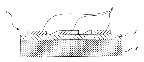
Fig. 1 illustrates schematically a photovoltaic facade element of the
i5 invention.
With further reference to Fig. 1, a photovoltaic facade element 1 comprises a
substrate 2 of the invention, a barner layer 3 on substrate 2, and a plurality
of
individual solar cells 4 in a series arrangement on barrier layer 3.
With respect to the production of thin-film semiconductor elements, especially
a o with their large area, the coating substrate surface according to the
invention
prevents or at least reduces the interdiffusion of substrate elements and
coating
elements. In addition, the substrate according to the invention makes it
possible to
cover over the local irregularities by the thin-film layers that are
deposited; this in
turn prevents short circuiting in the thin-film components deposited on the
a s substrate.
The coating substrate is e.g. a sheet-like, rolled substrate of aluminium or
its
alloys. Preferred are sheets, strips or foils of aluminium or its alloys. The
substrates may, however, be bodies of any desired shape having an aluminium
surface or a surface containing aluminium. The substrate may also be a
composite
3 o material, at least the outer layer of which is of aluminium or an
aluminium alloy.
A coating substrate may therefore feature a surface layer of pure aluminium,
CA 02250535 2003-05-29
-6-
containing essentially aluminium and the normal commercial grade impurities,
or
may be of aluminium alloys.
Substrates of pure aluminium may e.g. be an aluminium having a purity of 98.3
wt. % and higher, preferably 99.0 wt. % and higher and especially from 99.5 to
s 99.98 wt. %, the rest being commercially occurring impurities.
Wrought aluminium alloys are preferred for substrates of aluminium alloys.
Among these are for example alloys of the types: AIMg, AIMn, AIMgSi, AICuMg
and AIZnMg.
Wrought aluminium alloys may contain e.g.: up to 1.5 wt. % silicon, up to 1.0
wt.
i o % iron, up to 4.0 wt. % copper, up to 1.5 wt. % manganese, up to 6.0 wt.
magnesium, up to 7.0 wt. % zinc, up to 0.2 wt. % titanium, and up to 1.6 wt. %
of
other elements, the remainder being aluminium. Preferred are substrates of
aluminium containing: 0.25 to 1.5 wt. % silicon, up to 0.3 wt. % iron, up to
0.25
wt. % copper, 0.1 to 0.8 wt. % manganese, 2.7 to 5.0 wt. % magnesium, up to
1.0
1 s wt. % zinc, 0.01 to 0.2 wt. % titanium, up to 0.2 wt. % chromium, and up
to 1.5
wt. % of other elements, the remainder being aluminium.
Examples of aluminium substrate alloys used in practice are AlMg3, AlMg3Si,
AlMgS, AlMgSSi, A1Mg10 and AIMgSiI.
Useful as coating substrates are 5 ~.m to 1.5 mm thick foils, in particular 5
~,m to
a o 20 ~.m thick foils, or 0.5 to SO mm thick strips or sheets. Preferred are
aluminium
sheets, strips or foils of thickness 0.01 mm to 5 mm, and in particular 0.05
mm to
3 mm.
The substrates according to the invention permit thin-film systems--such as
intended for solar modules--to be deposited directly onto aluminium surfaces.
25 This makes possible e.g. the direct build up of photovoltaic modules on
facade
panels of commercially available aluminium or of commercially available
composite panels with aluminium outer layers (e.g. plastic core and honeycomb
core panels). Such photovoltaic facade elements satisfy the normal, high
standard
of requirements of the building industry and fire protection, whereby in the
case of
3 o fire the silicon solar cells in particular release no poisonous materials.
Further, the
production, operation and the disposal of photovoltaic modules on aluminium
substrates presents no ecological problems.
CA 02250535 2003-05-29
- 6a -
Facade elements with directly deposited thin-film solar cells make it possible
to
use facades for generating energy economically, at the same time reducing the
costs for installing and sealing solar modules. Such facade elements may be
employed in hybrid modes i.e. they can be used as solar collector panels, sun
s shades and as solar cells.
In a preferred version the substrate according to the invention features on or
in the
substrate surface to be coated at least partially an embossed type of
structure. The
embossed structure may be decorative in appearance or may be of such a form
that
it is possible to reflect the incident electromagnetic radiation, in
particular light, in
i o a predetermined direction.
CA 02250535 1998-09-30
The production of the embossed structure takes place preferably by use of
embossed rolls,
whereby e.g. in the production of the rolled substrate, the last rolling pass
is performed using
a roll with a surface exhibiting the desired structure; or by structuring the
coating.
Decorative embossed structures may contain logos, advertising texts, trade
marks, company
names or patterns, whereby embossed patterns may also be used e.g. to increase
the
difficulty of copying without permission. Such embossed structures exhibit
usefully a depth
of struct-ure of 1 nm to 1 pm, preferably between 10 nm and 0.5 Vim. By the
term depth of
structure is meant the maximum difference in height between structure valley
and structure
height.
Embossed structures for purposeful deflection or scattering of electromagnetic
radiation in a
predetermined range of angle may be employed e.g. to increase the efficiency
of the solar
cells. Such embossed structures exhibit usefully depths of structure of 0.5 pm
to 2 mm,
preferably from 10 ~m to 1 mm.
The embossed patterns may have any desired shape. The largest dimension of the
individual
elements of embossed structure parallel to the substrate surface is usefully
from 1 nm to 5
mm, preferably between 10 nm and 2 mm.
In photovoltaic applications the embossed structure is preferably a saw-tooth
pattern with V-
shaped troughs. The flanks of the V-shaped troughs are preferably such that
during the day,
at all times of the year, the sun shines on both flanks. For use in regions
not close to the
equator these V-shaped troughs are, therefore, preferably asymmetric in shape.
For applicat-
ions e.g. in regions in central Europe the V-shaped troughs are e.g. shaped
such that with
respect to the surface normals of the facade element one flank exhibits an
angle of ca. 5 to
10° and the other flank an angle of 50 to 60° (Angles referring
always to a full circle of
360°). The size of structure of the V-shaped troughs is usefully in the
millimetre or sub-
millimetre range.
Embossed surface structures, such as e.g. structures in the form of inverted
pyramids or
surface structures with saw-tooth patterns, increase e.g. in the case of
photovoltaic modules
the effective thickness of the solar cells so that the absorption capacity of
the cell increases.
The thickness of the thin film solar cell can thus be diminished with respect
to that of solar
cells on substrates without embossed pattern structures. As a result expensive
semiconductor
material is saved, the process of manufacturing the solar cells is accelerated
and in the case
case 2107 pct
CA 02250535 1998-09-30
-$-
of use of amorphous silicon modules it is possible to achieve a reduction in
the light induced
ageing of the cells and with that greater stabilised efficiency.
In a preferred version the rolled substrate may exhibit a barrier layer on the
substrate surface
to be coated, said barrier layer being a galvanic metal or metal oxide layer,
or a layer of
SiXNy, SiC or Zn0 the thickness of which is from 100 nm to 5 pm. A preferred
metal oxide
layer is e.g. a layer of aluminium oxide prepared by anodising.
In the case of a large area single module the barner layer may be in the form
of a conductive
material (e.g. Zn0); in the case of a conventional series arrangement of
individual cells, an
insulating layer must be provided between the actual module and the substrate
(e.g. sol-gel
or enamel layer)
In the following text we consider sol-gel layers to be layers that are
produced by a sol-gel
process.
In a further preferred version the rolled substrate may exhibit a sol-gel or
enamel layer as
barrier layer on the surface to be coated. The thickness of such a barrier
layer is e.g. 0.5 to
250 ~tm, usefully 1 to 200 Vim, and preferably 1 to 500 Vim.
The sol-gel layers have a glass-like character and besides the substrate's own
barrier layer
may be deposited between the actual cells also as front face (insulating)
closure of the cell
from the influence of weathering and fluids (acid rain, birds droppings etc.)
which promote
corrosion. The resistance to hailstones is provided as a result of the compact
composite of
sol-gel layer cell substrate.
The sol-gel layers made using a sol-gel process may on the one hand act as a
barrier layer
between substrate and cell; on the other hand, by applying substances
reflecting infra-red
radiation in combination with the conductive Zn0 back contact, they may be
used as a
means of reflecting infra-red radiation. As a result it is possible to save
the silver layer
which is otherwise employed.
White (infra-red-reflecting) coloured enamel layers may on the one hand act as
barner layers
between substrate and cell, on the other hand, by applying substances
reflecting infra-red
radiation in combination with the conductive Zn0 back contact, they may be
used as a
means of reflecting infra-red radiation. As a result it is possible to save
the silver layer
which is otherwise employed.
case 2107 pct
CA 02250535 1998-09-30
-9-
In order to improve the adhesive properties of sol-gel or enamel layers and to
prevent time
and temperature dependant diffusion of constituents of the barrier layer into
the aluminium
substrate or from the aluminium substrate into the barrier layer, the
aluminium substrate
may be anodised prior to coating. In that connection, the oxide layers formed
preferably
form an isotropic barrier layer with a thickness of 0.01 to 0.5 pm having a
dielectric constant
of 5 to 10. The isotropic barrier layer represents thereby a pore-free oxide
layer and exhibits
high resistance to elevated temperatures and increased chemical resistance
with respect to
alu-minium or aluminium alloys. Such an isotropic barrier layer prevents or
diminishes e.g.
any diffusion of adhesion inhibitors at the interface aluminium substrate /sol-
gel or enamel
layer.
An additional 0.1 to 10 p.m thick porous oxide layer may lie on the outer
surface of the
isotropic barrier layer. Foreseen thereby are in particular pores which are
open towards the
surface. A layer thickness of 0.1 to 2 ~m is preferred for the porous oxide
layer. The pores
preferably have a diameter of 0.03 to 0.15 p.m and a ratio of pore depth to
pore diameter of
usefully 10g to lOtz pores/cm2, preferably between 109 and lOtt pores/cmZ
Sol-gel layers contain e.g. polymerisation products of organic substituted
alkoxysiloxanes
having the general formula
R'Si(OR)3 or R'ZSi(OR)Z,
where R and R' signify a nyamic radical. In another version the sol-gel layer
may be ~ a
polymerisation product of organically substituted alkoxy compound having the
general
formula
XaAR4_n
where A signifies Si, Ti, Zr or Al, X signifies HO-, Alkyl-O- or Cl-, R
signifies phenyl,
alkyl, vinyl, vinylester or epoxyether and n represents a number 1, 2 or 3.
Examples of
phenyls are unsubstituted phenyl, for alkyl the same methyl, ethyl, propyl,
iso-propyl, n-
butyl, iso-butyl, pentyl etc., for -CH=CHZ, for -(CHZ)3-O-C(=O)-C(-CH3)=CH2
and for -
(CHZ)3-O-CHZ-CH=CH2.
The sol-gel layers are usefully deposited directly or indirectly onto the
aluminium substrate
by means of a sol-gel process. For that purpose, e.g. alkoxides and halogen
silanes are mixed
and, in the presence of water and suitable catalysts, hydrolised and
condensed. After remov-
ing the water and solvent a sol which forms is deposited on the substrate by
means of
case 2107 pct
CA 02250535 1998-09-30
- 10-
immer-sion, centrifuging, spraying etc. where it transforms into a film of gel
e.g. under the
influence of temperature and/or radiation. As a rule silanes are employed to
form the sol; it
is also possible to replace the silanes partially by compounds which instead
of silicon
contain titan-ium, zirconium or aluminium. This way it is possible to vary the
hardness,
density and refrac-tive index of the sol-gel layer. The hardness of the sol-
gel layer can also
be controlled by using different silanes, e.g. by forming an inorganic network
to control the
hardness and thermal stability or by using an organic network to control the
elasticity. A sol-
gel layer which can be classed between the inorganic and organic polymers can
be deposited
on the aluminium substrates via the sol-gel process by selective hydrolysis
and condensation
of alk-oxides, mainly those of silicon, aluminium, titanium and zirconium. As
a result of the
process an inorganic network is built up and, via appropriately derivitised
silicic acid esters,
it is possible to build up additional organic groups which may be used for
functionalising
and forming defined organic polymer systems. Further, the sol-gel film may
also be
deposited by electro-immersion coating according to the principle of
cataphoretic
precipitation of an amine and organically modified ceramic.
The enamel layers have a melting point in the range of 480°C up to or
close to the melting
point of the aluminium substrate. By close to the melting point is meant
temperatures of 20
or 10 °C below the melting point of the aluminium substrate. Suitable
enamel layers are
those based on alkali-silico-titanates, if desired with additions that lower
the stoving
temperature e.g. compounds such as oxides of lithium, barium, antimony,
cadmium, bismuth
or vanadium. Preferred are enamel layers from a frit containing the oxides of
silicon in
amounts of 27 - 33 wt. %, preferably 30 wt. %, of calcium, 9 - 12 wt. %,
preferably 9.5 -
11.5 wt. %, of titanium, 18 - 22 wt. %, preferably 20 - 22 wt. %, of sodium,
18 - 22 wt. %,
preferably 20 - 22 wt. %, of aluminium, 0.5 to 3.2 wt.%, preferably 2.8 - 3.2
wt. %, of
lithium, 3.5 - 4.2 wt. %, preferably 3.8 - 4.2 wt. %, of boron, 5 - 8 wt. %,
preferably 6.5 - 8
wt. %, of zirconium, 0.05 - 3 wt. %, preferably 2.3 - 3 wt. %, of zinc, 0.8 -
2.0 wt. %,
preferably 0.8 - 1.5 wt. %, of magnesium, 1 - 1.5 wt. %, of calcium, 0 - 5 wt.
%, of
antimony, 0 - 2.8 wt. %, of strontium, 0 - 1.5 wt. %, and phosphorous, 0 - 2.5
wt. %.
Preferred are enamel layers which are deposited as with additions a frit onto
the surface and,
by means of heat treatment or stoving, are converted into a layer of enamel
having a
thickness of 50 to 200 pm, preferably 50 to 120 p.m, in particular 70 to 100
p.m. The layer of
enamel may e.g. be produced from a mixture of oxides having the above
mentioned ratios of
constituents. As a rule the oxides are present in the form of frits i.e. as a
mixture which has
been ground. These frits may also contain processing additives such as e.g.
boric acid,
sodium meta-silicate, potassium hydroxide, titanium dioxide and pigments.
Typical
case 2107 pct
CA 02250535 1998-09-30
-11-
examples of a frit composition contains: 100 parts frit, about 4 parts boric
acid, one part
sodium meta-silicate, one part potassium hydroxide, five to fifteen parts
titanium dioxide
and one to seven parts pigment. The enamelling may e.g. comprise one layer,
whereby a
layer of frit composit-ion is deposited on the substrate surface and stoved in
a heat treatment
operation i.e. trans-formed to a layer of enamel. It is possible, however, to
have two layers
deposited in two stoving operations, three layers in three stoving operations
or several layers
in several stoving operations. Other methods for depositing enamel layers
consist of
depositing two or more layers of frit or frit compositions in only one stoving
operation. The
frit may e.g. have an average particle size of less than 74 Vim, usefully less
than 44 Vim. The
frits may be deposited by scattering, spraying, immersion, or slurry
deposition. Further
possibilities are electrostatic spraying or electrophoresis. In some cases in
which a
suspension agent is employed, the frit must be dried. After drying, the coated
substrate can
be placed in a stoving furnace in which the stoving operation may be carried
out
continuously or in stages. Typical stoving times are in the range of 3 to 10
minutes. Typical
stoving temperatures are between 480 and 560 °C. The stoving operation
may be performed
in stages or continuously.
Substrates according to the invention having a burner layer of gel or enamel
exhibit an
extremely smooth surface. Such barrier layers protect the substrate from the
harmful
influence of mechanical, physical, chemical and actinic effects and for
example to a large
extent from environmental effects. The surface is smooth, shiny and very hard.
The barrier layer on substrates according to the invention serves as a barrier
to diffusion
and/or as electrically insulating layer.
In a further preferred version the burner layer exhibits at least in part an
embossed structure
on its free surface. The embossed structure may be decorative in appearance or
it may be
made such that it is possible to deflect reflected incident electromagnetic
radiation, in partic-
ular light, in a predetermined direction. The shape of this embossed structure
corresponds
preferably with that of the previously described embossed structure on
aluminium substrate
surfaces.
The production of the embossed structure takes place e.g. by embossed rolling,
whereby a
roll with a desired embossed pattern is employed. In the case of sol-gel or
enamel barrier
layers embossing of the surface is carned out preferably with the barrier
layer in a semi-solid
state i.e. the embossing operation is carned out in the case of enamel layers
as an inter-
case 2107 pct
CA 02250535 1998-09-30
-12-
mediate step in the process during the stoving and in the case of sol-gel
layers when these
are in a partially hardened condition.
The substrate according to the invention is employed preferably for
manufacturing thin film
solar cells out of amorphous or poly or micro-crystalline silicon. Highly
preferred is for such
thin film solar cells to be deposited on facade elements. At elevated
temperatures, e.g. under
strong sunlight, solar cells normally exhibit a loss of efficiency. In the
case of semiconductor
materials a-Si and ~.-Si (poly or micro-crystalline) this is, however, much
less pronounced
than with monocrystalline silicon solar cells and e.g. in an a-Si:H is
typically 0.1 %/ °K.
This means that when employing such solar cells on facade panels, it is not
necessary to
provide circulation of air behind the panels in order to maintain the
efficiency of the cells.
This loss of efficiency must not be understood as having to do with limiting
the lifetime of a
solar cell or photovoltaic modules. Effects limiting the service life of such
solar cells are
exclusively corrosion as a result of poor sealing of the photovoltaic modules
and
interdiffusion of contact materials in the solar cell.
The deposition of the semiconductor film of amorphous, hydrated silicon and/or
of an alloy
of amorphous, hydrated silicon on the substrate according to the invention is
performed
preferably in a plasma chamber containing at least one pair of electrodes and
is coupled to
an electric high frequency generator, whereby the substrate is connected to a
first electrode
and a distance away from that electrode there is a second electrode and a gas
containing at
least one silicon compound is introduced into the plasma chamber, and a plasma
created
between the two electrodes by applying high frequency electric current with a
frequency of
10 to 150 MHz.
For precipitation of the semiconductor film the distance between the substrate
according to
the invention and the second electrode is preferably 1 - 3 cm. Also preferred
is for the ratio
of the frequency and the distance of the substrate from the second electrode
id between 30
and 80 MHz/cm. Highly preferred is for the frequency to lie between 30 and 100
MHz and
the distance of the substrate from the second electrode to be 1 - 1.25 cm. The
ratio of the
electrical energy emitted in the plasma - measured at the clamps of both
electrodes -and the
plasma volume available between the electrodes is preferably between 0.02 and
0.2 W/cm3.
The plasma deposition of the semiconductor film is preferably at a pressure of
10 to 50 Pa,
whereby the substrate temperature is usefully kept at 150 to 350 °C.
The gas introduced into
the plasma chamber preferably contains silanes or disilanes andlor higher
order silanes or
silicon tetrafluoride, or hydrogen, or mixtures of these substances. The
silane gas is intro-
duced at a throughput rate of 0.3 to 2.0 scan (cm3 NTP/min) per litre of
useable space in the
case 2107 pct
CA 02250535 1998-09-30
-13-
plasma chamber and preferably around 1.2 sccm/litre. The gas introduced into
the plasma
chamber may contain further substances such as e.g. germanium, hydrogen,
argon, german-
ium tetrafluoride, methane, carbon tetrafluoride, nitrogen, ammonia,
phosphines or di-
boranes.
Highly preferred is the precipitation of a semiconductor film of an alloy of
silicon and
nitrogen. In that case the gas introduced into the plasma chamber comprises a
mixture of
silanes and ammonia in a volume ration of 0.03 to 0.3, and the distance of the
substrate
according to the invention from the second electrode is 1 to 3 cm.
The process-related objective is solved by way of the invention in that the
substrate surface
to be coated is exposed to a chemical brightening process or a plasma etching
process.
Plasma etching includes plasma etching with radicals which react with the
surface and form
gaseous components, or physical plasma etching (sputtering off), whereby the
surface is
removed as a result of bombardment with e.g. Argon ions.
Commercially available aluminium alloys often contain nucleants such as e.g.
titanium
diboride. Such nucleants normally produce a grain structure on the surface
which is usually
sharp edged and, after alkaline or acidic cleaning of the surface, leads to
trough-shaped
recesses around the grain. Such recesses can as a rule not be covered over
satisfactorily by
plasma deposited layers. As result local short circuiting can occur between
the back and
front contact.
Before depositing thin films, the sharp edged grains are, therefore, according
to the
invention rounded off e.g. by ion bombardment in an Ar-plasma. Further, such a
treatment
provides better thermal contact between such a grain structure and the
substrate material, as
a result of which the interdiffusion of coating material and substrate
material during the
coating process is reduced.
In general metals exhibit a polycrystalline structure. As a result of the Ar-
ion bombardment
of the substrate surface during the physical plasma etching process, the metal
surfaces obtain
an essentially amorphous structure. In turn, such amorphous substrate surfaces
result in low
interdiffusion behaviour.
Bombarding the aluminium substrate surface with high energy, heavy argon ions
in a plasma
process leads therefore to an amorphous substrate surface and to rounding off
of the sharp-
edged, grain structure at the surface of the substrate.
case 2107 pct
CA 02250535 1998-09-30
-14-
Another preferred process for preventing sharp edged recesses is according to
the invention
to clean the surface using a chemical plasma etching process in an atmosphere
which does
not attack the substrate surface to be coated chemically. Specially preferred
for that purpose
is an atmosphere of 02-, SF6, 02/SF6, CF4-, 02/CF4- or BCL3.
Also preferred is a process in which the substrate exhibits a barrier layer,
the thickness of
which is selected such that the local irregularities present are completely
covered over by
this barrier layer, and namely such that there is no longer any sharp edged
irregularities
present. Suitable for that purpose are in particular ZnO, SiN, SiC and sol-gel
layers
deposited in a sol-gel process, and enamels. Such layers exhibit an extremely
smooth surface
and at the same time act as good barrier layers against diffusion and as
insulating layers.
The process according to the invention is effective in reducing the
interdiffusion of substrate
elements and thin film coating elements, and makes it possible to cover
irregularities com-
pletely by the thin film coating. As a result it is possible to deposit less
expensive diffusion
barriers and insulating layers, whereby such barrier layers produce a further
effect by
rounding off irregularities on the substrate surfaces.
25
35
case 2107 pct