Note: Descriptions are shown in the official language in which they were submitted.
CA 022~0810 1998-10-01
W O 97137S12 PCTAUS97/03849
S~-AXIS SURROUND SOUND PROCESSO~
Wl'l~l IMPROVED MATR~ AND CANCELLATION CONTROL
R~ ~lr~round of the Invention
The present invention relates in general to processors for the
periphonic reproduction of sound. More specifically, the invention relates to
improvements in the detector filter, separation matrix, low frequency center
front cAncçllAtion circuit, servologic control voltage generator, voltage
controlled Amplifiers, and output shelf filter circuits of a su~l..ulld sound
processor for multi~hAnnel redistribution of audio signAl.q.
A ~ulloulld sound processor operates to çnhAnce a two-channel
stereophonic source signal so as to drive a multiplicity of loudspeakers
arranged to sullo~d the listener, in a mAnner to provide a high-definition
solmtlfield directly comparable to discrete multitrack sources in perceived
performance. An illusion of space may thus be created enabling the listener
to experience the fullness, directional quality and aural 11im~n.qion or
"spaciousness" of the original sound environment. The foregoing so-called
periphonic reproduction of sound can distinguished from the operation of
conventional solmtl~eld processors which rely on digitally generated time
delay of audio signAl.q to simulate reverberation or "ambience" associated
with live sound events. These conventional systems do not directionally
localize sounds based on information from the original performance space
and the resulting reverberation characteristics are noticeably artificial.
To accomplish this end, a surround sound processor typically
comprises an input matrix, a control voltage generator and a variable
matrix circuit.
The input matrix usually provides for balance and level control of the
input ,si~nAl.q, generates normal and inverted polarity versions of the input
.qi~nAl.~, plus sum and difference ,signAl.~, and in some cases generates
phase-shifted versions, and/or filters the si~nAl.~ into multiple frequency
ranges as needed by the r~mAinrler of the processing requirements.
The control voltage generator includes a directional detector and a
~ervologic circuit. The directional detector measures the correlations
CA 022~0810 1998-10-01
WO 97137512 PCT/US97/03849
between the .qignAl.q which represent sounds encoded at dirrelel~t directions
in the stereophonic sound stage, generating voltages corresponding to the
prednminAnt sound location. The servologic circuit uses these sign~l.q to
develop control voltages for varying the gain of voltage-controlled Ampli~ers
in the variable matrix circuit in accordance with the sound direction and
the direction in which it is intended to reproduce the sound in the
o~ (lin~ loudspeakers.
The variable matrix circuit includes voltage-controlled ~mplifiers and
a separation matrix. The voltage-controlled Amrlifiers amplify the input
matrix audio sign~l.q with variable gain, for application to the separation
matrix, where they are used to selectively cancel crosstalk into different
loudspeaker feed si~n~lq. The separation matrix comhines the outputs of
the input matrix and of the voltage-controlled Amplifiers in several dirre. e~ltways, each resulting in a loudspeaker feed sign~l, for a loudspeaker to be
positioned in one of several different locations ~ullo~ 1ing the listener. In
each of these signAl.~, certain signal components may dyn~micAlly
elimin~ted by the action of the detector, control voltage generator,
voltage-controlled Amplifiers (VCA's) and separation matrix.
In surround sound processors, much of the subtleties of the
presentation are due to the characteristics of direction detector and
servologic circuit of the control voltage generator and of the VCA's. As
these are further refined, the apparent performance becomes more
transparent and effortless-solm-lin~ to the listener.
Sllmm~ry of the Invention
The present invention provides an improved surround processor for
the reproduction of sound from a stereophonic source in a manner
comparable to a live presentation from multiple sources in performances.
The present invention relates in particular to im~lovelllents in
implementation of several portions of the ~ullo~ d sound processor
;ui~y, including im~l. velllents in the implementation of the circuitFy of
the direction detector, separation matrix ~ ;uilly, center front bass
cancellation circuit, servologic control voltage generator employing
CA 022~0810 1998-10-01
WO 97137512 PCT/US97/03849
multiple-axis control voltage signAl.q, voltage controlled ~mplifiers, and
output shelf filter circuits of ~urloulld sound processor.
In one emborliment, the invention comprises a ~u~ ulld sound
processor including audio input terminAl.q for receiving a left and a right
audio input signal forming a conventional stereophonic audio signal pair; an
~ input stage for buffering and bAlAnting the left and right audio input
signAlq and providing output left and right audio .qignAl.q; a detector filter
circuit receiving the output left and right audio .qignAl.q and having a band
pass characteristic, followed by an inverter circuit and a detector matrix
circuit to provide left and right audio signal currents; a direction detector
circuit receiving the left and right audio signal currents and providing
th~ler.~ left-right and front-back directional signAl.q, and including peak
hold ~ ;uill y, a detector splitter circuit providing left front-right front, left
back-right back, and front-back output signAl.q derived from the outputs of
the direction detector circuit, and incorporating linearity correction
circuitry; a servologic circuit providing variable time constant smoothing of
the output .si~nAl.q from the detector splitter circuit, and producing six
output control .qignAl.q; voltage controlled Amplifier circuits, each controlledby a different one of the six output control signAl.q of the servologic circuit,and each provided with input audio .signAl.q that are a comhinAtion of the
left and right output audio signAl.q from the input stage, each of such
voltage controlled Amplifier circuits being provided with an inverter circuit
so as to produce controlled audio .qignAl.q of both normal and inverted
polarity; a separation matrix circuit for comhining the output left and right
audio .qignAl.q from the input stage with one or more of the output .qignAl.q
from the voltage controlled Aml-lifier circuits in various appropriate
proportions so as to provide a plurality of matrix output signAl.q; and a like
plurality of output buffer amplifiers for buffering and level control of the
~ matrix output signAl.q to produce at a like plurality of output terminAl.q a
set of loudspeaker feed .qignAl.q for Amplification and application to
loudspeakers placed in a listening area so as to surround a listener.
CA 022~0810 1998-10-01
W O 97/37512 PCT~US97/03849
A technical advantage achieved with the invention is a :~ul . oulld
processor which provides faster but smoother and more realistic
multichannel sound redistribution from a stereophonic source.
Another advantage achieved is an improved aural performance in
terms of reduced artifacts and anomalies in the redistribution of
stereophonic sound into a multich~nn~l soundfield.
Brief Description of the Dra~ings
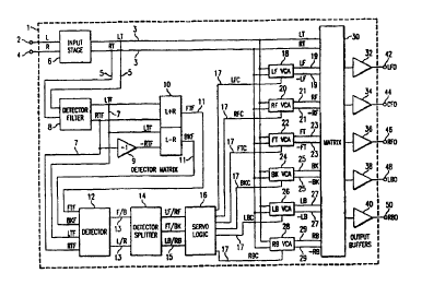
FIG. 1 is a block schematic of a six-axis sulloulld sound processor
according to the invention;
FIG. 2 is a detailed srh~m~tic of an improved detector filter circuit
employed in the processor of FIG. 1;
FIG. 3 is a graph of the frequency response of the improved filter
also showing the frequency response of the previously used filter for
comparison;
FIGS. 4 is a detailed schematic of the separation matrix .,ircuilly of
the processor of FIG. 1, including center front bass cancellation circuitry;
FIG. 5a, 5b and 5c are detailed schçm~tics of the control voltage
generator circuitry of the processor of FIG. 1, showing modified component
values for improved performance characteristics;
FIG. 6 is a detailed schematic of improved VCA circuitry employed in
the processor of FIG. 1;
FIG. 7 is a detailed schematic of an output shelf filter employed in
the processor of FIG. 1; and
FIG. 8 is a graph of the frequency response of the shelf filter circuit
of FIG. 8.
Detailed Description of the Invention
The principal new features of the present invention are an improved
detector filter circuit providing a better match between the detector
performance and the audibility of concurrent sounds in different frequency
ranges; an illl~ oved separation matrix c*cuit resulting in reduced artifacts
and anomalies in the pelceived performance; improved bass cancellation
;ui~ly to remove bass from the center front loudspeaker; improvements
CA 022~0810 1998-10-01
WO 97/37512 PCTIUS97/03849
to the component values of the control voltage generator ~ilcuiLly to attain
faster and smoother performance characteristics; new VCA ~ ;uilly with
improved characteristics over the type previously used; and new output
shelf filter circuitry for better spatial representation in certain sulloulld
sound modes of operation.
In the present invention, based on experience with the ~ ;uilly of
the processor of FIG. 1, further iml~lovements have been made in the
detector filter ci. ~;uilly. It has been found that gain-riding ~ uilly in the
separation matrix is no longer needed and better aural performance is
obtained with some changes in the separation matrix coefficients. Previous
center front bass cancellation circuitry has also been improved to provide
better reduction in bass output in the center front ch~nnt3l, which is
typically applied to smaller loudspeakers having lower bass power h~n(lling
capacity. Furthermore, the time constants in the control voltage generator
circuitry have been adjusted to faster values in order to improve dynamic
separation and attain a faster response. Previous VCA circuits employed
junction field-effect transistors for gain control, but the present invention
includes an improved VCA circuit based on an integrated circuit voltage
controlled ~mplifier. To improve the sense of spaciousness and depth in
rear ch~nnel sounds, shelf filters have been provided with improved
frequency response characteristics, for use in certain modes of sound
reproduction. To understand these improvements more fully, the ~l~r~led
embodiments of the invention will be described in detail below.
In FIG. 1, the surround sound processor 1 is equipped with input
ter~nin~l.c 2, 4, for receiving left (L) and right (R) audio input sign~
respectively. These ~ign~ are processed by an input stage, 6, typically
cont~ining auto-bAl~ncing circuitry and other signal conditioning circuits,
such as level controls and possibly a panorama control. The output ~ign~
from this stage are labeled LT and RT, and are applied via lines 5 to a
detector filter 8, and via lines 3 to VCA's 18 - 28 and an separation matrix
30. Although not shown, to simplify the drawing for improved clarity, the
CA 022~0810 1998-10-01
WO 97/37512 PCT/US97/03849
inversions of these siFnAl.q, -LT and -RT may be generated here and also
provided via lines 3 to the VCA's 18-28 and separation matri~ 30.
The detector filter 8 provides filtered .~ignAl.q LTF and RTF labeled 7
to the inverter 9, the detector matrix circuit 10 and to a detector circuit 12.
The signal RTF is inverted by the inverter 9 and also applied to the
detector matrix circuit 10. The detector matrix 10 generates outputs 11
labeled FTF and BKF corresponding to front (L+R) and back (L-R) signal
directions. These signAlq are also applied to detector circuit 12, which
comprises two identical circuits. One accepts input .si~nAl.q FTF and BKF
and produces an output signal F/B at 13, while the other accepts the input
.si~nAl.q LTF and RTF to produce an output signal L/R at 13.
The detector output fii~nAl.c 13 labeled F/B and L/R are applied to the
detector splitter circuit 14, wherein are produced the three qignAl.q 15
labeled LF/RF, FT/BK and LB/RB. These in turn are applied to the servo
logic circuit 16 to provide six control voltage fii~nAl.q 17 labeled LFC, FRC,
FTC, BKC, LBC and RBC, for controlling the six VCA's 18 and 28, and
labeled LF, RF, FT, BK, LB, and RB VCA respectively.
These VCA's receive the LT and RT signals 3 in different proportions,
according to the directional matrix they are intended to provide, and apply
their output si~nAl.q 19 through 29 each in both polarities to the separation
matrix 30, which also receives the unmodified LT and RT .cign~ 3. As
mentioned above, though not shown in FIG. 1, inverters may also be
provided ffir these fiiFnAl~ LT and RT to generate -LT and -RT respectively.
These inverters may be considered to be a part of the input stage, as their
outputs may also be applied to some inputs of VCA's 18 through 28. These
details are shown in the accompanying FIGs. 2-8, as necessary for the
underst~n(1inF of the invention, but are not included in FIG. 1 in order to
simrlify the diagr~m and improve clarity.
Outputs from the matrix 30 are passed through variable attenuators
31 through 3~t and buffered by AmplifiP.rs 32 through 40, providing output
.~ignAl.~ LFO, CFO, RFO, LBO and RBO at terminAl.~ 42, 44, 46, 48 and 50
respectively. These form the five standard outputs of the processor 1, but
CA 022~0810 1998-10-01
W 0 97/37512 PCTrUSg7/03849
other outputs (not shown) may also be provided. Typically, the outputs
shown may be provided to electronic crossover components in order to
provide subwoofer o~ ul~ L-SUB, R-SUB and M-SUB (not shown in FIG.
1) as well as the five outputs shown. Such techniques are well known in
the art and need no further e~pl~n~tion here.
Referring to FIG. 2, there is shown an improved detector filter
circuit. Previous detector filters used in ~imil~r processors which are the
subject of related Patent Applications Lefe~ellced above employed an inverse
Fletcher-Munson curve, which appro~im~tes the sen~ilivi~y of the ear
particularly at low levels. Experience has shown that there was too much
crosstalk, or too little separation, below lkHz, and the modified circuit
responds better to these lower frequencies.
In FIG. 2, which corresponds with FIG. 4 of the co-penlling
application, there is shown a detector filter 8, inverter 9, and detector
matrix 10. Input termin~l.c 90 and 92 are provided for receiving the ,si~nAl.
5 labeled LT and RT respectively. These ,ci~n~l.q 5 are filtered by the
detector filter first stage 8 comprising operational Amplifier OA301 and its
associated components for the signal LT, and op-amp OA302 with its
associated components for the signal RT. Other outputs of this filter stage
8 are passed to the inverter 9 and to the detector matrix 10. The right
channel filter output is inverted by inverter 9 which comprises op-amp
OA303 with input resistor R309 and feedback resistor R310, with typical
values shown. The output of op-~mp OA301 is fed via resistor R311 and
capacitor C309 in series to output terminal 108, providing a filtered current
signal LTF. The output of op-amp OA302 is fed via resistor R316 and
capacitor C317 to output terminal 110 providing the filtered current signal
RTF. The outputs of both op-amps OA301 and OA302 are combined via
resistors R314 and R315 and capacitor C311 to provide the filtered current
signal FTF at output terminal 100, and the outputs of op-amps OA301 and
OA303 are comhin~d via resistors R312 and R313 and capacitor C310 to
provide the filtered current signal BKF at output terminal 102.
CA 022~0810 1998-10-01
W 0 97/37512 PCTAUS97/03849
This circuit is .~imil~r to detector filters disclosed in Fosgate's earlier
patents and patent applications, cited above, but the components formerly
shown in FIG. 4 of the co-pen-ling application 08/276,902, labeled C305,
R305, C306 and R306, have been removed from the circuit. Additionally,
capacitors C303 and C304 have been changed from 0.01uF to 0.022uF and
resistors R303, R304, R307 and R308 have changed to 49.9k ohms from
200k ohms and 110k oh_s. These changes effect the alteration in
frequency response from an inverse Fletcher-Munson curve to a band-pass
filter without the boosted response in the upper midrange region.
Additionally, resistors R309, and R310 in the inverter circuit 9 have
changed from 24.9k ohms to 10k ohms, without ch~ngin~ the inverter
function or gain.
In the final stage 10 the resistors R312 through R316 have changed
from 4.0~.kohm.s to 20kohms, and capacitors C310 and C311 changed from
0.47uF to 0.1uF. Resistors R311 and R316 changed from 2.00k ohms to
13.3k ohms and capacitors C309 and C312 changed from 0.47uF to 0.068uF.
In all cases the time constants are approximately the same as previously,
but the sensitivity of the left-right detector has been reduced by almost 3dB
relative to the sensitivity of the front-back detector. These changes tend to
lock in dialog better than previously, since dialog is often placed in the
center front chAnnel.
Referring to FIG. 3, there is shown a graph of the frequency response
of the detector filter of FIG. 2, on which is also shown as a broken curve the
corresponding frequency response for the inverse Fletcher-Munson filter of
FIG. 4 of copen(lin~ Patent Application No. 08/276,901 for comparison.
It can be seen that the response of the filter of the present invention,
labeled B, is about 5dB more sensitive to midrange audio frequencies than
that of the previous filter curve, labeled A. It is also about 5dB less
sensitive to low bass frequencies, minimi7ing the effects of these
frequencies which are not audibly loc~li7.~hle, and therefore detract from
correct localization of midrange frequencies if they are allowed to interfere
with directional detection.
CA 022~0810 1998-10-01
WO 97/37S12 PCT/US97103849
In FIG. 4 is shown a ç~ncell~tion matrix forming part of the
separation matrix circuit 30. By comparison with FIGs. 10a, 10b, 11a and
11b of the co-penllin~ Patent Application 08/276,901, it will be seen that the
matrix circuit has been considerably qimplified. In particular, the gain-
riding connections have been ~limin~ted, and the "corner logic kill" switches
and resistors have also been removed.
Furthermore, the matrix is configured to operate either in a 4-axis
mode or a 6-axis mode. Additionally, not shown in FIGs. 4a and 4b, the
rear rh~nnel.q are configured to operate in Dolby ~ oLuld/THX mode or in
Mono mode for reproduction of monophonic audio.
There are six principal outputs provided by the matrix, as in previous
circuitry. In the previous circuitry, the matrixing resistors fed a common
virtual ground at the input of an op-amp buffer, before applying the outputs
to the level control and output amplifying stages shown in FIG. 1. In the
revised circuitry, these buffers are absent, and the matrix resistors each
sum into a common point before being applied directly to the volume control
circuitry. Either method is equally valid, and the principle of superposition
ensures the equivalence of these two approaches to the same end.
In FIG. 4, resistors R401 through R408 sum ~3irre~ellt proportions of
each of eight ,qi~n~l.q applied to the input termin~l.q labeled LT, -RT, RB,
BF, -FT, -LB, -BK and RF, respectively. The common junction of these
resistors is the terminal labeled LF 6-AXIS. To determine the effective
coefficients, each resistance plays into the total of all the r~m~ining
resistors in parallel, so each coefficient is the quotient of the conductance ofthe corresponding resistor divided by the total conductance of all eight
resistors. Thus the coeffir.ient for LT is 0.1mS divided by 0.6269mS =
0.1595, and so for a left signal, in absence of the other fiign~ls (some of
which may be present) will produce an output at LF of 0.1596 times the LF
input.
It may be convenient to normalize the coefficients to this gain value,
by dividing each of the coefficients calculated as in the ~xz~mple above by
the value 0.1595, so that the relative coefficients are 1 for LT, the left total
CA 022~0810 1998-lO-01
W O 97/37512 rCTAUS97/03849
input; 0.2551 for -RT, the right total input, which is added here to broaden
the sound stage, as discussed in others of the related Patent Applications;
0.6667 for RB, the right back VCA output; 1 for BF, the bass cancellation
filter (so that logic control does not affect the low bass frequencies); 0.7519
for -FT, the front VCA negative output, for center front ç~ncell~tion; 1.1001
for -LB, the left back VCA negative output, for left back c~ncell~t.ion; 1.2407
for -BK, the back VCA negative output, for center back c~ncell~tio~; and
0.2551 for RF, the right front VCA output, for cancellation of the -RT signal
fed to the left front output through R402.
By .cimilAr reasoning, the coefficients for each of the rem~ining
sections of FIG. 4 are easily calculated. As the matrix has left-right
sym~netry, the center front and only one of left or right signal sets need to
be calculated.
The inputs to each section of the matrix are, as intlic~ted above, the
unmodified left and right total sign~l.q LT and RT, and their inversions -LT
and -RT; the output of the bass cancellation filter BF, which is derived from
the -FT VCA output with an inverting amplifier in the filter; and the six
output pairs of the six VCA circuits, LF, RF, LB, RB, FT and BK, with
their inversions -LF, -RF, -LB, -RB, -FT and -BK. These .~ign~l.q will be
m~imi7:ed when their respective VCA control si~n~l.q LFC, RFC, LBC,
RBC, FTC and BKC in FIG. 1 are at their mA~imum values, respectively.
The output termin~l.q in FIG. 4 are labeled LF 6-AXIS, RF 6-AXIS,
LB 6-AXIS, RB 6-AXIS, CF, LB 4-AXIS, RB 4-AXIS, LF 4-AXIS and RF 4-
AXIS. For the four corner .qign~ , LF, RF, LB and RB, CMOS analog
switches (not shown) select either 4-axis or 6-axis mode of operation,
routing either the 4-AXIS or the 6-AXIS si~n~l.q to the corresponding output
gain controls and buffer ~mpli~ers (not shown). The center front matrix is
the same in either case and thel~role needs no switch.
In FIG. 4, the center front bass cancellation circuit is also shown. At
bass frequencies, the resistors R423 and R424 are small in comparison to
the impedance of capacitor C401, so that the FT signal is passed through
them to the CF output, where it cancels the LT and RT si~n~l.q applied
CA 022~08l0 l998-lO-Ol
W O97/37512 PCT~US97/03849
through resistors R417 and R418. At higher frequencies, the capacitor
shunts this signal to ground, thus allowing the LT and RT sign~ to be
comhined into the CF output. Note that this circuit simply removes bass
from the center front loudspeaker, but it can be disabled by means of the
CMOS switch S401, which short-circuits capacitor C401 and the~erole
removes the bass input frequencies that would otherwise be present, thus
allowing a full-range loudspeaker to be used in the center front dialog
~~h~nnel
FIG. 5 shows the revised control voltage generator circuit. The
principal change here is the inclusion of a peak-hold c*cuit between the
logarithmic ratio detectors and the detector splitter circuit. In addition, the
front-back and left front-right front output stages of the detector splitter
have been modified to add linearity correction, effected by the zener diodes
and resistors in their feedback loops, to better match the characteristics of
the new VCA circuits to be described below.
In FIG. 5a is shown the detailed schematic of the direction detector
circuit 12 which comprises two identical log ratio detector circuits. By
comparison with FIG. 5 of the co-pending Patent Application No.
08/276,901, the topology is .cimil~r, but some important changes have been
made. In each of the two input stages, OA501 and OA502 and associated
components, a 22m ohm resistor R501, R502, has been added in parallel
with the diodes D404-D404, which limits the dynamic range of the log ratio
detector for very small signal levels.
In the previous circuit, capacitors C401 and C402 were placed at the
anodes of D405 and D406 and the cathodes of D407 and D408 respectively,
to serve as very short term peak detection capacitors; these have been
removed from the present circuit.
The values of resistors R507 through R612 are different from their
counterparts in the previous circuit, R405 through R410, and capacitors
C501 and C502 are 4.7uF instead of 1uF (C403 and C404) in the previous
circuit. Additionally, the capacitors C40~ and C406 and resistors ~411 and
R412 of the previous circuit have been removed. The effect of these
CA 022~0810 1998-10-01
WO 97137512 PCT~US97/03849
changes is that the detector now has a peak-hold characteristic with an
attack time constant of about 0.5ms and a decay time constant of about
4.7ms.
In the output ~mplifier of FIG. 5a, the resistor R513 is now about a
twelfth of its former value, partly because the resistors in the interstage
network have been considerably reduced The zener diodes D409 and D410
in the previous circuit have been removed, and instead, the operational
amplifier is connected to reduced supply voltages to limit the output voltage
swing.
The components used to trim detector balance, resistor R514 and
potentiometer R515, have also been reduced in value from R413 and ~415
of the previous circuit.
Although different operational amplifiers have been used in the
present circuit, they result in at least some im~ ve~llent in performance,
relative to those of the previous ~ ;uiLly.
The significant performance advantage of this new detector over the
previous c*cuit is that it responds much faster than before, and it
effectively responds to the peaks of the log ratio detector output instead of
the average, resulting in higher values of the control .~ign~ and hence
greater dynamic separation of the different spatially located domponents of
the input audio .sign~
In FIG. 5b, as compared with FIG. 6 of the co-pending application,
the alternate modes of operation previously selected byt a switch S506A
through S505F is no longer employed, .simplif~ing the circuit considerably.
The CMOS switches S501 and S502 formerly connected so as to "kill"
logic action havè also been removed from the new circuit. The CMOS
switches S503 and S504 connected to kill corner logic while permitting
front-back logic to operate have also been removed. Instead, a pair of
CMOS switches S521 and S522 have been added to switch between 4-axis
and 6-axis modes of operation.
In FIG. 5c, which shows a revised servologic circuit comparable to
FIG. 8 of the previous application, the revosed VCA's do not require the six
12
CA 022~0810 1998-10-01
WO 97/37512 PCT/US97/03849
operational ~mplifiers configured as ideal rectifiers that were used in the
previous circuit (U803, U804, U808-9, U813-4 of the previous application's
FIG. 8). These have been ~limin~ted.
The capacitors C801 etc. following the servologic switches S801-3 in
FIG. 8 have been changed in FIG. 5c from .22uF to 1uF, but the following
30k ol~m/ .01uF networks such as R802 and C802 have been removed. The
3K resistors R801 etc. were changed to 4.99K. The net effect is that a
shortest time constant of 5m.~ is achieved, the longest being about 28ms.
This range is generally faster than in the previous version of the servologic
circuit.
A significant change is the addition of a diode D559 across the
servologic switch S552 in the front logic ~h~nnel This has the effect of
dramatically speeding up the attack time for front channel dialog.
FIG. 6 shows the new VCA ~ uilly in a representative schematic.
All of the VCA's have identical c-l~;uilly, except that the back VCA has an
added transistor switch circuit to shut o~ its operation when desired.
The new VCA comprises an integrated circuit U601 of commercially
available type SSM6120A, from Analog Devices. The components
surrolln-ling this VCA are necessary for its proper operation. The input to
this VCA is shown as the signal BIN, which is a comhin~tion of LT with -
RT in equal proportions, through 49.9k ohm resistors not shown in FIG. 6.
This is the back channel input signal. The output current of U601 drives
the virtual ground input of U602, which has resistor R610 in its feedback
loop, and capacitor C602 to minimi7~e high frequency noise. This amplffler
provides the -BK output to the separation matrix of FIG. 4, while Amplifier
U603 with resistors R611 and R612 provides the inversion of this .signz~l,
i.e. BK, to the separation matrix.
At the lower part of FIG. 6 is shown a transistor switch, comprising
transistors Q601-2, with resistors R613-6. When this switch is activated by
a logic high on the BK VCA KILL terminal, this VCA is reduced to zero
gain. This function is only necessary in some modes of operation of the
13
CA 022~0810 1998-10-01
W O 97~7512 PCTrUS97/n3849
~U~ U ld sound processor, and is only required for the center back signAl,
so the five other VCA's do not include these components.
FIG. 7 shows a schematic representative of the shelf filters provide
din the rear chAnnçl.q of the processor. This filter comprises an operational
Amplifier U701, with input resistor R701, and feedback comprising R702
and the series combination of R703 and C701. The frequency response of
the filter is shown in FIG. 8.
The main function of this filter is in reducing sihil~nt splash into the
back channels from front dialog. It also has the effect of increasing the
apparent psychoacoustic depth of the sound reproduced in the back
~,hAnnel.q .
While the embodiments shown herein are representative of the most
preferred variations of the circuitry of a ~ ound sound processor according
to the present invention, it will be apparent to those silled in the art that
many modifications and variations of the ~ ;uil~y emborlim~ntq may be
made without departing from the spirit of the present invention.