Note: Descriptions are shown in the official language in which they were submitted.
°
CA 02250958 1998-10-20
1
bIETHOD AND APPARATUS FOR REDUCTING POWER DISSIPATION IN
DC TERMINATION CIRCUIT
Field of the Invention
This invention pertains to telephone line interface
circuits. More particularly, the invention pertains to
DC termination devices for limiting tip-to-ring current
on a telephone line.
Background of the Invention
In two-wire telephone communication systems, a pair
of wires, termed tip and ring, respectively, carry a DC
current which may be used for powering devices, such as
telephones, coupled across the wires. Tip and ring also
carry actual telephone signals, such as voice or modem
signals. A voltage source at the central office of the
telephone company provides a voltage across the tip and
ring nodes so as to provide the aforementioned DC
current. The wires connecting the telephone to the
central office, of course, have a finite impedance.
Accordingly, the length of wire between the central
office and a particular telephone dictates the actual
tip-to-ring voltage and current that the telephone
receives. Thus, a telephone that is close to the
central office (has a short distance of wire
therebetween) normally will receive a higher voltage and
therefore greater current than a telephone which is
coupled to the central office through a longer wire
connection.
Certain international standards, for example,
international standard TBR 21 of the European
Telecommunications Standard Institute (ETSI) require
that the tip-to-ring current through any
telecommunication device not exceed a specified current
level. TBR 21, for instance, specifies a maximum tip-
to-ring current of a telecommunications device of 60
- CA 02250958 1998-10-20
2
milliamps. However, the standard also requires that,
below 60 milliamps, the telecommunication device
provides a constant impedance to the tip-to-ring line
such that tip-to-ring current through the device will
vary linearly with tip-to-ring voltage presented to the
device.
Although many factors contribute to the
establishment of such standards, one of the primary
reasons for specifying a maximum tip-to-ring current is
to reduce the power which the central office must
generate in order to provide the DC tip-to-ring current
to telecommunication devices coupled to the central
office.
International standard TBR 21, as of the writing of
this specification, has not been officially adopted, but
is being highly recommended.
In view of international standard TBR 21 and other
standards containing tip-to-ring current limit
specifications, telecommunication equipment must be
provided with front end DC termination circuitry for
limiting tip-to-ring current through the device. Such
circuitry usually takes the form of a current limit
circuit that provides a constant resistance up to the
specified current limit and thereafter provides a
constant current at the specified current limit as the
voltage continues to rise. For example, from 0 to 60
milliamps, tip-to-ring current through the device
increases linearly with tip-to-ring voltage. However,
when the current reaches 60 milliamps, the current will
remain constant at 60 milliamps as the tip-to-ring
voltage increases further.
Telecommunication devices commonly employ a current
sink that may dissipate excess power when the tip-to-
ring currents are high. Such current sinks may require
a heat spreader or some other means of dissipating the
heat buildup in the active components (commonly termed a
' CA 02250958 1998-10-20
3
heat sink) in order to avoid heat damage to the current
sink. Heat sinks consume a significant amount of
volume. Many telecommunication devices, for example,
PCMCIA card modems are extremely small. Thus, the need
for large heat sinks is a significant problem since it
will reduce the space available for other desirable
electronic componentry.
A tip-to-ring voltage of 60 volts, for example,
would not be unusual in most countries. Accordingly,
with a tip-to-ring voltage of 60 volts and a tip-to-ring
current of 60 milliamps, up to 3.6 watts of power will
be dissipated in the telecommunications device. 3.6
watts is a significant amount of power to dissipate,
thus requiring a fairly large heat sink. In a compact
piece of equipment in which various electronic circuits
are closely packed together, the heat put out by the
heat sink might adversely affect the operation of, or
even destroy, neighboring electronic circuitry.
Accordingly, it is an object of the present
invention to provide an improved DC termination device.
It is another object of the present invention to
provide a DC termination device which can meet the
performance requirements of various standards.
It is a further object of the present invention to
provide an improved DC termination device for a
telecommunications device which can meet the
specifications of various standards and minimize power
dissipation in the device.
Summary of the Iaveatioa
The invention is a method and apparatus using
digital signal processing for limiting tip-to-ring
current through a telecommunications device responsive
to tip-to-ring voltage. In particular, the invention is
a DC termination device comprising a voltage controlled
' CA 02250958 1998-10-20
4
current source coupled across the tip-to-ring lines and
controlled by the local digital signal processor
responsive to the detected tip-to-ring voltage on the
line. The tip-to-ring signals, include the DC tip-to-
ring current, and AC currents which comprise the audio
band transmit and receive signals. The tip-to-ring
signal is amplified and converted by an analog to
digital converter. The AC and DC components of the tip-
to-ring signal are digitally filtered and applied to
digital signal processing circuitry. The DC component
of the signal is digitally filtered and forwarded to
digital signal processing circuitry that determines the
DC tip-to-ring voltage. When the digital detection
circuitry detects a tip-to-ring voltage that would
produce a current of less than the specified maximum
current, the digital signal processor adjusts the tip-
to-ring voltage via the voltage control inputs of the
voltage controlled current source to cause it to operate
essentially as a constant impedance, thus providing a
linear relationship between tip-to-ring voltage and tip-
to-ring current through the device. This mode is termed
the constant impedance mode.
However, when the DC tip-to-ring voltage crosses
the designated threshold, indicating that the tip-to-
ring current will exceed 60 milliamps, the circuitry
enters a constant current mode. In this mode, the
digital signal processor generates a control signal for
the voltage controlled current source to cause it to
maintain the tip-to-ring current at a specified current
value regardless of the detected tip-to-ring voltage.
The signal is provided to the voltage controlled current
source, through appropriate conditioning, amplification
and digital to analog converting circuitry.
The constant current provided in the constant
current mode need not be the maximum threshold current,
but can be any arbitrarily selected current.
Accordingly, in a preferred embodiment of the invention,
CA 02250958 2000-09-15
rather than causing the maximum threshold current to be the
constant current, the constant current is set at or near
the minimum operational current in order to minimize power
dissipation in the device. In such an embodiment, when the
5 device switches to the constant current mode, the drop in
tip-to-ring current will be accompanied by an increase in
tip-to-ring voltage. Thus, when in the constant current
mode, and the voltage drops below a second voltage
threshold indicative of the fact the voltage provided by
the central office would produce a current of less than 60
milliamps if in the constant impedance mode, the digital
processing circuitry switches back to the constant
impedance mode.
In accordance with one aspect of the present invention
there is provided a telecommunication device comprising: DC
termination circuit for controlling a current through said
telecommunication device as a function of a DC voltage
supplied to said telecommunication device as at least
portion of a telecommunication over a telecommunication
network, said DC termination circuit comprising: a voltage
controlled current source coupled across said DC voltage
supplied to said telecommunication device having a control
input; means for determining said DC voltage supplied to
said electrical circuit by said voltage source; means,
coupled between said means for determining and said control
input of said voltage controlled current source, for
supplying a control voltage for controlling said voltage
controlled current source as a function of said determined
voltage.
In accordance with another aspect of the present
invention there is provided a method of controlling the
current through an electrical device as a function of a
voltage supplied to said device comprising: providing a
voltage controlled current source to control the current
CA 02250958 2000-09-15
5a
through said device; determining said voltage supplied to
said device; when said voltage supplied to said device is
below a first predetermined value, controlling said voltage
controlled current source to present a constant impedance
to said voltage source; when said voltage supplied to said
device crosses from below to above said first predetermined
value, controlling said voltage controlled current source
to drain a constant current from said voltage source; and
when said voltage supplied to said device crosses from
above to below a second predetermined value, controlling
said voltage controlled current source to present a
constant impedance to said voltage source.
Brief Description of the Drawings
Figure 1 is a graph illustrating an exemplary tip-to-
ring current versus tip-to-ring voltage relationship for a
telecommunications device of the prior art containing no
current control circuitry.
Figure 2 is a schematic diagram of a DC termination
device of the prior art.
Figure 3 is a graph illustrating an exemplary tip-to-
ring current versus tip-to-ring voltage relationship for a
telecommunications device having a typical tip-to-ring
current control device of the prior art.
Figure 4 is a graph illustrating an exemplary tip-to-
ring current versus tip-to-ring voltage relationship
for a telecommunications device constructed in accordance
with the present invention.
CA 02250958 2000-09-15
5b
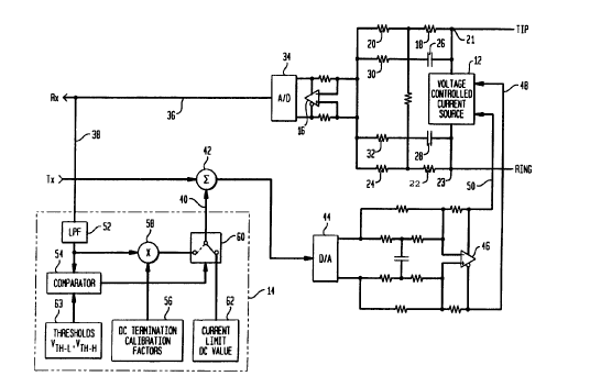
Figure 5 is a block diagram illustrating a DC
termination device constructed in accordance with the
present invention.
Figure 6 is a graph illustrating an alternate
exemplary tip-to-ring current versus tip-to-ring voltage
CA 02250958 1998-10-20
6
relationship for a telecommunications device constructed
in accordance with the present invention.
Detailed Description of the Invention
Figure 1 is a graph illustrating an exemplary tip-
s to-ring current versus tip-to-ring voltage relationship
for a telecommunications device of the prior art
containing no current control circuitry. Without any
particular current control circuitry, the
telecommunication device presents essentially a constant
impedance to the circuit. Accordingly, the tip-to-ring
current to tip-to-ring voltage relationship is a
straight line of slope I, as illustrated in Figure 1.
Thus, a telecommunication device of this design which is
coupled close to a central office, and therefore,
receives a higher tip-to-ring voltage, will draw more
current than a device positioned further away.
At least in part due to this, standards have been
promulgated which require that telecommunication devices
contain a DC termination circuit for preventing the
device from drawing current from the tip-to-ring lines
exceeding a specified threshold value. One prior art
solution to providing this characteristic is a current
sink circuit with a corresponding heat sink. An example
of such a circuit is shown in Figure 2. It comprises a
transistor 2 having its source to drain terminals
coupled across tip and ring and a Zener diode 4 coupled
between ring and the base of the transistor in order to
prevent the current from tip-to-ring from exceeding a
threshold level specified by the value of the Zener
diode 4.
The characteristics of a telecommunication device
containing such a current control DC termination device
would be as shown in Figure 3. As can be seen, the
device will have a constant impedance characteristic
below the specified threshold current. However, above
' CA 02250958 1998-10-20
7
the specified threshold current, further increases in
the tip-to-ring voltage will not affect the tip-to-ring
current, which will remain at the threshold current. In
this device, even though the threshold current is not
exceeded, there is still significant power dissipation
when the tip-to-ring voltage is high because the tip-to-
ring current is maintained at the absolute maximum
threshold current value.
Figure 4 illustrates a desirable tip-to-ring
current to tip-to-ring voltage relationship for a two-
wire telecommunications device. As can be seen from
Figure 4, the desired characteristics are that the
telecommunications device presents a constant impedance
to the line when the tip-to-ring voltage is below a
specified threshold V.~_L. When the tip-to-ring voltage
exceeds VTx-L, the telecommunications device presents a
variable impedance to the line such that, above V.LH_L, the
tip-to-ring current remains constant for any value of
tip-to-ring voltage. In this manner, the tip-to-ring
current is guaranteed never to exceed a specified
current dictated by the selected value of V.~_L. The
constant current may be set to the current LLH_L.
However, preferably, in order to minimize power
dissipation, the constant current level is maintained at
or near the minimum current needed to assure proper
operation of the telecommunications device on the line
or the minimum current allowed by any applicable
performance specifications, whichever is higher. It
will be apparent to those of skill in this art that, in
the latter embodiment, since V=IR (voltage is equal to
current times resistance), when the apparent line
resistance decreases as the tip-to-ring voltage
increases from just below VTH-z to just above V.~_L, the
tip-to-ring voltage will increase discontinuously. This
is because the relationship V=IR holds under all
circumstances. Thus, when the tip-to-ring voltage
exceeds V.LH_L.and the telecommunications device enters the
constant current mode, the tip-to-ring voltage will jump
CA 02250958 1998-10-20
8
to a value higher than VTx-H. The exact value of VTx-H is
a function of VTx-z and the newly chosen lower operating
current. More generally, the tip-to-ring voltage to
current relationship changes as the device switches from
a constant impedance mode to the constant current mode.
Accordingly, when the device is in the constant current
mode, VTx-z is no longer the voltage indicative of when
the tip-to-ring current would be below L~ if the device
were in the constant impedance mode. Rather, a much
higher tip-to-ring voltage, V~_H, will signify that, if
operation is reverted back to the constant impedance
mode, the tip-to-ring current would be below LLH.
Due to the increasing miniaturization of electronic
components, including componentry both in and separate
from integrated circuit packages as well as the
increasingly more common employment of digital signal
processing technology in telecommunications devices, it
is now possible to provide substantial additional
functionality with minimal increase in cost or circuitry
by simply adding functionality in the digital signal
processor. Particularly, since a digital signal
processor is embodied in the apparatus and typically is
so fast as to be able to perform substantially more
processing in a given time period than is needed for
basic operation, the digital signal processor can be
programmed to perform many functions which previously
were performed by separate circuitry.
The present invention takes advantage of the
existence of digital signal processing in the device to
provide the current to voltage relationship illustrated
in Figure 4.
Figure 5 is a functional block diagram of the
pertinent circuitry for a two-line telecommunications
device in accordance with the present invention. In
order not to obfuscate the invention, Figure 5 shows
only the circuitry relevant to the DC termination
CA 02250958 1998-10-20
9
circuitry for controlling the tip-to-ring current across
the device. However, it should be understood that,
although not shown in the figure, the device typically
contains circuitry which is actually powered by the DC
tip-to-ring voltage available across nodes 21 and 23.
The functionality of the present invention is
embodied primarily in voltage controlled current source
(VCCS) block 12 and control block 14. It should be
understood that, while the block diagram of Figure 5
illustrates the functionality of the circuit in terms of
specifically identified circuit components or blocks,
preferably the functionality illustrated within control
block 14 is provided by a programmed DSP and not
necessarily by distinct circuit components. On the
other hand, of course, the invention can be implemented
by distinct circuit components.
In any event, the tip and ring terminals are
coupled to the device at nodes 21 and 23. VCCS 12 is
coupled across nodes 21 and 23. The tip-to-ring current
may include any one or more of (1) the DC tip-to-ring
current, (2) an AC feedback current, (3) a DC feedback
current, and (4) an AC audio band signal comprising the
actual data being transmitted and/or received. The tip
and ring lines are coupled to the infinite impedance
(theoretically) of the complementary input terminals of
a differential amplifier 16, as well as to the VCCS 12.
The AC signal path to the differential amplifier is
through resistors 18, 20, 22 and 24. The DC signal path
to the differential amplifier is through capacitors 26
and 28 and resistors 30 and 32. The amplified signal is
provided to an analog to digital converter 34. The
output 36 of the A/D converter 34 is provided to a
digital signal processor for extraction and processing
of the receive audio band data signal, the DC feedback
signal, and the AC control signal. The digital signal
on line 36 is thus indicative of the DC tip-to-ring
voltage. Accordingly, the signal on line 36 also is
CA 02250958 1998-10-20
provided through signal path 38 to control circuitry 14.
Control circuitry 14 includes circuitry for determining
the tip-to-ring DC line voltage and generating a control
voltage output on line 40 which will be used to control
5 VCCS 12.
Control circuit 14 comprises a digital low pass
filter 52, a digital comparator 54, a DC termination
calibration factor 56, a multiplier 58, a switch 60, a
voltage source circuit 63 for generating the threshold
10 voltages, and two voltage sources 62 and 63. In
operation, the digital signal is applied to a low pass
filter 52 to extract from the signal on line 38 only the
DC tip-to-ring voltage component. The output of the
filter 52 is applied to the comparator 54 and to a
multiplier 58.
Comparator 54 compares the DC tip-to-ring voltage
to the pre-determined values V.~_L or V~_H supplied by
voltage generator 63. Voltage generator 63 selects the
value to be applied to the comparator, i . a . , V.~_L or VTH_
H, responsive to the mode in which the termination device
is currently operating. Specifically, when in the
constant impedance mode, voltage generator 63 applies
V.~_L to the comparator 54 for comparison with the tip-to-
ring voltage. When in the constant current mode,
voltage generator 63 applies V.~_H to the comparator 54
for comparison with the tip-to-ring voltage. The output
of the comparator 54 controls a switch 60 which switches
the control circuit 14 between the two modes of
operation, namely, constant impedance mode and constant
current mode. Particularly, when control circuit 14 is
in the constant impedance mode and comparator 54 detects
that the tip-to-ring voltage has crossed from a value
below V~_L to a value above V.~_L, it controls switch 60
to switch from the constant impedance mode (the mode
shown in solid in Figure 5) to the constant current mode
(the mode shown it dotted outline in Figure 5).
CA 02250958 1998-10-20
11
When control circuit 14 is in the constant current
mode and comparator 54 detects that the tip-to-ring
voltage has crossed from above VTH-H to below VTH-H, it
causes switch 60 to switch back to the constant
S impedance mode.
As can be seen from Figure 5, when control circuit
14 is in the constant impedance mode, the tip-to-ring DC
voltage received from the line filtered by low pass
filter 54 and applied to multiplier circuit 58 where it
is multiplied with an appropriate DC termination
calibration factor from DC calibration factor circuit
56. The DC termination calibration factors generated by
circuit 56 are merely appropriate scaling factors to
cause the voltage on line 40 (and thus on control lines
48 and 50) to be in an appropriate value. The output of
the multiplier 58 is applied through the switch 60 to
control DC control voltage output line 40 for
transmission to the voltage control lines 48 and 50 of
VCCS as described more fully below. Thus, in constant
impedance mode, the control voltage for VCCS 12 that is
placed on control voltage line 40 for transmission to
the control voltage terminals of the VCCS 12 is simply a
conditioned and properly proportioned version of the
tip-to-ring voltage received over the line. This will
cause the current-to-voltage relationship to behave as
illustrated in Figure 4 for values of tip-to-ring
voltage below V.~_L.
When control circuit 14 is in the constant current
mode (shown in solid outline in Figure 5), a constant DC
voltage is applied to line 40 through switch 60.
Accordingly, the DC control voltage applied to line 40
for controlling VCCS 12 will be constant. This, in
turn, will cause the voltage controlled current source
to allow a fixed and unvarying current to pass through
the VCCS from node 21 to node 23. Thus, the tip-to-ring
current through voltage controlled current source 12 is
CA 02250958 1998-10-20
12
maintained constant when the tip-to-ring voltage is
above VTx-H
The VCCS control voltage on line 40 is first summed
by summing circuit 42 with the audio band transmit
signal which is received from the audio digital signal
processing circuitry. The audio digital signal
processing circuitry, of course, may actually be
comprised of the same digital signal processor that
generates the control voltage on line 40. The output of
the summing circuit is provided to a digital to analog
converter 44 for conversion to analog form. It is then
amplified by differential amplifier 46 and applied to
VCCS 12 via lines 48 and 50. Within VCCS 12, the DC
control voltage is extracted by appropriate filtering
and applied to the voltage control terminals where it
controls the tip-to-ring current through the VCCS (from
node 21 to node 23). The AC audio component of the
signal on lines 48 and 50 is applied directly to the
tip-to-ring nodes 21 and 23 for transmission back to the
central office.
The DC termination calibration factor circuitry 56
and the voltage source 62 can be designed to provide
almost any current-to-voltage relationship desirable.
The relationship illustrated in Figure 4 and described
herein is merely one preferred example. Also, the
invention has been described with respect to a two-wire
telecommunications device designed to perform in
accordance with ETSI standard TBR 21. However, it
should be understood that the device can be used in many
other telecommunication applications as well as non-
telecommunication applications. The device can be used
as the front end for any device which should have a
desired current-to-voltage relationship.
Even further, the circuitry illustrated in control
block 14 may be comprised of individual circuits, may
simply be part of the functionality of a programmable
CA 02250958 1998-10-20
13
digital signal processor, or even may be part of the
functionality of a digital signal processor existing in
the circuit for additional reasons, such as processing
of the audio band data signals. Even further, the
functionality shown in block 14 may be provided by a
finite state machine.
In certain applications, it may be desirable to
enter the constant current mode whenever the tip-to-ring
voltage indicates that the tip-to-ring current would
exceed the minimum current necessary to assure reliable
operation of the device. Such operation would keep
power consumption in the device to a minimum. Figure 6
is a graph illustrating such a current-to-voltage
relationship. However, many of the standards, such as
the ETSI international standard TBR 21, have certain
performance requirements which require a current-to-
voltage relationship as illustrated in Figure 4 which
would not be met by a current-to-voltage relationship as
illustrated in Figure 6.
Having thus described a few particular embodiments
of the invention, various alterations, modifications,
and improvements will readily occur to those skilled in
the art. Such alterations, modifications and
improvements as are made obvious by this disclosure are
intended to be part of this description though not
expressly stated herein, and are intended to be within
the spirit and scope of the invention. The foregoing
description is by way of example only, and not limiting.
The invention is limited only as defined in the
following claims and equivalents thereto.