Note: Descriptions are shown in the official language in which they were submitted.
CA 022~1084 1998-10-21
HIGH ~ ;1) DATABUS UTILIZING POINT TO MULTI-POINT
INTERCONNECT NON-CONTACT COUPLER TECHNOLOGY ACHIEVING A
MULTI-POINT TO MULTI-POINT INTERCONNECT
s
10 ~IELD OF INVENTION
The present invention relates tO a high speed databus lltili7ing point to multi-point
interconnect non-contact coupler technology achieving a multi-point to multi-point
interconnect. It is particularly conc~llled with a fault tolerant, high speed, low latency bus
15 allowing multiple circuit packs sharing a comrnon backplane or midplane to be interco~n.~c~
and have a multi-gigabit per second bandwidth.
BACKGROUND OF THE INVENTION
Non-contact, such as capacitive or inductive or directional, coupler technology has
been suggested as a method of improving the pelroll.lance and the functionality of data and
colll.llunications interconnect busses. However, few practical means have been provided by
which these capacitively or inductively or directionally coupled buses can provide multi-point
tO multi-point connections between various circuit packs connected to the bus.
-
CA 022~1084 1998-10-21
U.S. Patent no. 3,619,504 to De Veer et al. issued November 9, 1971 discloses a
high speed data tr~nsmi.csion network employing directional coupling elements that are spaced
along a ~lA~ .ccion line to couple hlfollllation from the ~ .s...;csjon line to taps. De Veer
discloses ~ ion lines with a single source and a plurality of sinks or, conversely, a
5 single sink and plurality of sources. De Veer also discloses a dual multiplex system for
interconnf~cting two source circuits with two sink circuits. Source clc.llellls are respectively
connf~cted to tr~ncmicsion lines. Spaced along each tr~ncmiscion line are two directional
couplers, one connPcted to each sink circuit. Thus, a sink circuit is connf~cted to more than
one stub line and is capable of receiving signals origin~ting from both sources.
U.S. Patent No. 5,638,402 to Osaka et al. issued June 10, 1997, discloses a bus
transceiver or databus. It employs capacitive and inductive coupling between bus connector
lines. Further, it discloses a plurality of two way circuits coupled through a non-contact bus.
U.S. Patent No. 5,365,205 to Wong issued November 15, 1994 discloses a backplane
databus u-ili7ing directional couplers. The tr~ncmicsion line or conductive loop is termin~tf~
by a termination resistor in the circuit card which includes the driver for the tr~n.cmi.ccion
line.
CA 022~1084 1998-10-21
SUMMARY OF THE INVENTION
An object of the present invention is to provide an improved high speed databus
utili~ing point to multi-point interconnect non-contact coupler technology achieving a multi-
S point to multi-point inle.co~ ect. In one aspect a bus is provided that el;...;i~ s contention
between signals tr~ncmitte~ along dirre~ell~ial signal lines. This type of contention is
typically found on a two-way bus.
In one aspect there is provided a databus comprising: at least one con~ucting layer;
a plurality of slots; each slot having a plurality of termin~l.s; one of said plurality of t~.. ;.. ~lc
comprising a source terminal for connec~ion to a source; said source terminal conn~octe-l to
a tr~n.cmicsion line; said tr~ncmic.cion line, having an outbound portion and a return portion;
said tr~ncmicsion line, along its outbound portion, being a part of a single con-~ucting layer
of said at least one con-1ucting layer; said tr~n.cmicsion line extending from the slot; another
15 of said plurality of terminals colllplisillg a sink terminal for connection to a sink; said sink
terminal conn.octe~l to a tap; said tap extPn~ing proximate to a tr~ncmi.csion line origin~ting
from a different slot, said tap being coupled with a non-contact coupler to the tr~n.cmiccion
line origin~ting from a different slot.
In another aspect there is provided a databus comprising: a first con~lucting layer and
a second con-lucting layer separated by an incnl~ting layer; a first slot having a plurality of
. . . , _ _
CA 022~1084 1998-10-21
tPrTnin~l.c; one of said plurality of terminals COlllp~iSillg a first terminal for connection to a
first source; said first source terminal conn~ctecl to a first tr~ncmi.csion line; said first
tr~n.cmicsion line extPn~ling from the first slot; said first ~ ..,ic~ion line having an outbound
portion and a return portion; said first tr~ncmi.csion line, along its outbound portion, being
5 a part of the first con~ cting layer; another of said plurality of te~...i..~l.c of the first slot
comprising a first sink terminal for connection to a first sink; said first sink t~orTnin~l
conntoctecl to a first tap; said first tap e~tton~ling proximate to a second tr~ncmicsion line
origin~ting from a second slot, said first tap being coupled by a non-contact coupler to the
tr~ncmi.csion line origin~ting from said second slot; said second slot having a plurality of
10 terminals; one of said plurality of termin~ls collll,lisillg a second source tPrmin~l for
connection to a second source; said second source terminal connt~cting to said second
tr~n.cmi.csion line; said second tr~ncmicsion line having an outbound portion and a return
portion; said second tr~n.cmicsion line extending from the second slot; said second
tr~n.cmic.cion line, along its outbound portion, being part of the second con~1ucting layer;
15 another of said plurality of terminals in the second slot comprising a second sink terminal for
connection to a second sink; said second sink terminal connlocted to a second tap; said second
tap extending proximate to a tr~ncmi.csion line origin~ting from a different slot, such that said
second tap is coupled with a non-contact coupler to a tr~n.cmicsion line origin~ting from a
different slot.
CA 022~1084 1998-10-21
BRIEF DESCRIPIION OF DRAWINGS
The invention will be further understood with the following description with
references to the drawings in which
Figure 1 is an exploded schP~tic view of a databus in accolda lce with an
embodiment of the present invention; and
Figure 2 is a schPrn~tic view of a databus in accordance with another embodirnent of
the present invention.
DETAILED DESCRIPI ION OF THE PREFERRED EMBODIMENTS
A databus allows circuit packs, such as computer processors or memory, to exchange
information by way of electric or electromagnetic signals. A databus has a number of
connectors or slots where each individual circuit pack makes electrical connection with the
databus. A slot is a series of terminals, typically in the nature of pinhole connectors, to
receive a series of pins from a single circuit pack connector. A databus typically is made
20 up of a number of alternating con~ cting and incul~ting layers with each con~ucting layer
having a series of contiUcting traces. When a circuit pack connector is inserted into a slot,
. .
CA 022~1084 1998-10-21
each pin enters a pinhole and makes connection with one terminal on each of the conrlucting
layers. rhe location on the con~lcrinp trace where the electrical connection is made with
the pin is a te~nin~l. A pin will typically pass through a number of con~1ucting and
in~nl~ting layers. Where there is no electrical connection desired between a te~ AI and
5 another part of a con~lllcting layer, there is no con-ln~ting trace etched between the t~.lll;~l~l
and any other part of that con~l~lcting layer. Alternatively, a pin may be penT~nPntiy
attached to a terminal and extend through other layers and the surface of the databus. Such
a pin is then inserted into a pinhole connector in a circuit pack.
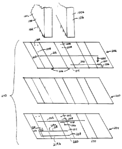
Figure 1 shows an exploded perspective view of a databus 240, which is one
embo~iment of the present invention. The databus comprises alternating layers of etched
con~ cting material 202,204 and in.~ul~tin~ material 207. The in~ ting layer 207 prevents
electrical signals from travelling between one con~lucting layer 202 and another con-lucting
layer 204. As will be appreciated bv those skilled in the art, in~ul~ting layer 207 could
15 comprise a ground plane sandwiched between two in~ul~ting sheets.
The databus 240 has a plurality of slots 206. These slots 206 have a plurality of
terminals 208. A circuit pack connector 100 may be plugged into each slot. The circuit
pack connector 100 has pins 102 to electrically connect it to the terminals 208 in the slot.
20 These pins allow the circuit pack connector 100 to transmit or receive data to or from the
CA 022~1084 1998-10-21
databus 240. When data is tr~n~mitted on the databus 240 from a circuit pack in a slot it is
received by another slot where another circuit pack is connPcted
One of the tPrmin~l.c 208 in a first slot 209 comprises a first terrninal 210 for
S connPction to a first source. This first source is a pin on a circuit pack connecLol 100a in
the slot 209 which sends data signals. The first source terminal 210 is connPcted to a first
tr~n.cmi~cion line 212. The first tr~n~mi.~sion line 212 extends from the first slot 209. The
first tr~n~mi.~sion line 212 along its entire extent is a part of the first con~1ucting layer 202.
A plurality of tr~n~mi.~sion lines could be associated with each other, forming, for example,
at least one pair of dirÇele-llial signal lines and a pair of clock signal lines. The clock signal
deterrnines the sampling instant at the sink terminals when signals tran~mitted on the databus
240 are to be processed. In another implementation, such clock signals may be ernbPd~Pcl
within the tr~n~mittecl signals by various encoding schemes, obviating the need for a
separately tr~n.~mirte(l clock.
Another of the plurality of terminals 208 of the first slot 209 comprises a first sink
terminal 214 for connection to a first sink. The first sink terminal 214 is connPcted to a first
sink which is another pin on the circuit pack connector 100a that receives data. It should be
noted that the terminals of a slot need not be located on the same con-lucting layer. For
example, first sink terrninal 214 is on con-lurting layer 204 whereas the first source tPrrnin~
210 is on condllcting layer 202. The first sink terminal 214 is connPcte(l to a first tap 216.
CA 022S1084 1998-10-21
This first tap 216 extends proximate to a second tr~n~mic~ion line 218 that origin~t~s from
a second slot 220 such that the first tap is coupled with a non-contact coupler, such as a
directional or c~r~eitive or inductive coupler, to the second L~ C~ion line 218 ori~ g
from the second slot 220. Tr~n~mi.c.sion line 218 has an outbound portion 219a COIlly~ g
the part which passes by taps such as first tap 216 and a return portion 219b which extends
from beyond the last tap to the termination of the tr~n.~mi~.~ion line. The return portion 219b
could be part of the same con~lucting layer 204 or a different con~ cting layer, such as
con~lcting layer 202. The second slot also has a plurality of terminals 208. One of this
plurality of terminals comprises a second source terminal 224 which is connPcted to the
second tr~n.cmi~ion line 218. The second source terminal 224 is for connection to a second
source which is a pin on the circuit pack connector 100b plugged into the second slot 220.
The second tr~n~mi~ion line 218 extends from the second slot and is along its entire extent
part of the second con~cting layer 204. Another of the plurality of terminals in the second
slot 220 comprises a second sink terminal 226 for connection to a second sink. The second
sink terminal 226 is connPctecl to a second tap 228. The second tap 228 extends proximate
to a tr~n.cmicsion line 232 origin~ting from another slot 230 such that the second tap 228
receives signals from tr~n~mi~sion line 232 origin~ting from slot 230.
Figure 2 shows a srh~m~tic of a databus 300 in accordance with another embodiment
of the present invention. Databus 300 has a plurality of slots 302a, 302b, .. 302n. As
shown in Figure 2, this embodiment of the invention allows circuit packs that utilize non-
CA 022~1084 1998-10-21
contact coupler technology to send data to and receive data from other packs in slots in the
same databus. In other words, although any single tr~ncmiccion line is point-to-multipoint,
multi-point to multi-point tr~ncmiccion of signals in the databus is achieved. For example,
this is achieved by routing the ~ csion line 304 from a source te,.--il-~l 306 in a slot
302c past taps 308, 312, 316 ~rt~.he~ to sink terminals 310, 314, 318 in every other slot
3021, 302m, 302n to which multi-point co...---~ iC~tion is desired for that tr~ncmiccion line
304. As a slot 302c can have a plurality of taps 320, 322,324, it can receive data from
tr~n.cmicsion lines 326, 328, 330 origin~ting in a plurality of other slots 3021, 302m, 302n.
In this way multi-point to multi-point hllelco,~ection is achieved despite use of non-contact,
10 point-to-multipoint coupler technology.
As well it should be noted that a slot could have a plurality of source terminals. Each
source terminal would be connected to a different tr~n.cmi.csion line which could be routed
past the same or different slots.
A benefit of the present invention is that the source terminals only transmit data and
the sink terminals only receive data. This elimin~tes contention at the bus level, typically
found on a two-way bus.A further benefit of the present invention is that the outbound
portion of each tr~n.cmiccion line from a particular slot may be etched on a single conductive
20 layer. This reduces signal reflections that could occur when a signal passes from one
conductive layer to another and ensures that the delay between signals tlAI-.c~ e~
CA 022~1084 1998-10-21
sim--lt~n.oously along differential signal lines and along clock signal lines is Illi~.i...i,~d
Signal distortion and reflection can prevent a databus from operating at higher bit rates. A
minim~l delay is irnportant as it helps to ensure that sink terminals receiving a signal from
a ~ sion line will receive the signal within a predictable tirne period after it is
5 trancmilted
A tr~n.cmi.csion line is termin~ted in a number of different ways, for exarnple, the
means for termination of a tr~n~mi.csion line 218 comprises a terrnination terminal 238 in the
slot where the tr~n~mi.~sion line originates. In other words, the tr~n~mi~.cion line 218 loops
10 back around and is termin~ted on a tc~ &~ion terminal in the same slot where it origin~t-od.
This provides the advantage of improving fault tolerance in the databus.
Another means for termin~ting a tr~n~mi~sion line is illustrated by trancmi~sion line
212 which has a resistor 234 connected to ground. A further means of te~ g a
15 trancmi~sion line is illustrated by tr~n~mi~sion line 242 which has a connection through a
resistor 237 to the supply plane 236. This provides the advantage of allowing the termination
to be electrically biased to the supply plane 236. Although for illustrative purposes different
tr~n.~mic.sion lines are shown with different types of terminations, typically, for any given
databus, all tr~n~mi~sion lines will be termin~ttod in the same fashion.
- 10 -
.,
CA 02251084 1998-10-21
A databus in accordance with the present invention could be implennPntto~l on one
con~l1cting layer.
Numerous mo-iific~tions, variations and adaptations may be made to the particular
S embo~im~nt~ of the invention described above without det)~li~g from the scope of the
invention which is defined in the claims.