Note: Descriptions are shown in the official language in which they were submitted.
CA 022~1160 1998-10-02
W O 97/37755 PCTrUS97/05841
I
PLATE FOR REACTION SYSTEM
The present application is a continuation-in-part of U.S. Application 08/630,018,
5 filed April 9, 1996, titled '~Plate for Reaction System,~' U.S. Application 08/730,636, filed
October 11, 1996, titled "Liquid Distribution System and U.S. Application 08/744,386,
filed November 7, 1996, titled "Liquid Distribution System."
The present invention relates to a plate having formed thereon numerous small-
scaled reaction cells (or wells) that are formatted to allow the cells to be individually
10 addressed despite their small size, to allow each cell to accommodate a substrate for
reactions, to allow each cell to be separately ilhlmin~ted for optical detection, and to
allow sufficient material between reaction cells to support the formation of an appropriate
seal between the plate and an ancillary device, for instance a liquid distribution device that
delivers reagents to the reaction cells.
Recent advances in microfluidics, i.e., the small-scale transfer of liquid amongcompartments, have made it possible to conduct reactions such as syntheses or assays in
very small-scale devices. See, for instance, Zanzucchi et al., "Liquid Distribution
System," U.S. Patent Application No. 08/556,036, filed November 9, 1995. Such devices
allow the progr~mming of the concurrent operation of thousands of separate reactions.
20 Pursuant to the Zanzucchi et al. patent application, such an apparatus can be used to
distribute various liquids to thousands of reaction cells, which reaction cells can be
fabricated on a plate.
In recent years, drug discovery programs have focused on the use of microtiter
plates having 96 or 384 cells to assay prospective pharmaceuticals in an in vilro model for
25 a pharmaceutical activity or for conducting small-scale syntheses in parallel. The devices
provided for by the advances in microfluidics, however, are to be used to conduct
reactions at, for example, I ,000, 10,0000, 100,000 or more reaction sites or cells. By the
present invention, these sites or cells are located on a plate. In attempting to operate at
the scale implied by these numbers of reaction cells, one must take into account, among
30 other things, (1) the need to form seals that allow fluid to be transferred to each cell
without cross-contamination from fluid intended for another cell, (2) the need to provide
a cell aperture widths sufficient to facilitate fluid transfer, (3) the need for the cells to have
CA 022~1160 1998-10-02
wO 97/37755 PCT/US97/0584
- 2 -
sufficient cross-sectional area and volume to allow for optical detection, (4) the need to
have a relatively compact plate that is easily stored and operates with a liquid distribution
device that moves liquids through relatively compact distances and (5) the need for
sufficient alignment and cell separation to allow the cells to be individually identified. By
the present invention, these needs are met with a "nanotiter" or "small-scaled" plate
having reaction cells that are densely packed.
SUMMARY OF THE INVENTION
The invention provides a plate having a plurality uniformly sized reaction cellsformed in its upper surface, wherein the density of the reaction cells is at least about 10
10 cel}s per cm2. Preferably, the reaction cells are arrayed in rows and columns. Also,
preferably, the plate is rect~ng~ r, preferably with the rows and columns of cells parallel
to the edges of the plate. Preferably, the area of each of the openings (i.e., apertures) of
the reaction cells is no more than about 55% of the area defined by the multiplication
product of (I ) the pitch between reaction cells in separate rows and (2) the pitch between
15 reaction cells in separate columns. The product between this row pitch and column pitch
can be termed the "footprint" of a cell, meaning the amount of area supporting each cell
of a plate. More preferably, this aperture area is no more than about 50%, yet more
preferably 45%, of the cell footprint. Preferably, the density of cells is no more than
about 350 per cm2, more preferably no more than about 150 per cm2, yet more preferably
20 no more than about 120 per cm2. Preferably, the density of cells is at least about 10 cells
per cm2, more preferably at least about 20 cells per cm2, more preferably at least about
40 cells per cm2, still more preferably at least about 100 cells per cm2.
The footprint, which is symmetrically overlaid on the cell, encompasses plate
surface area on all sides of a cell. The minimlml distance from the edge of the cell to the
25 boundary of the footprint is here termed the "seal strip width," since this is the area on
which à gasket material can be applied. In one preferred embodiment, the density of cells
is from about 10 to about 45 cells per cm2, more preferably about 10 to about 20 cells per
cm2, and the seal strip width is from about 300 lam to about 1,000 ~m, more preferably
from about 600 !lm to about 1,000 ~um.
Preferably, the diameter or width of the aperture of a cell is about 400 ~lm to
about 1100 ~m, more preferably about 900 ~m to about 1100 llm. The depth of the cells
CA 022~1160 1998-10-02
W O 97/37755 PCT~US97/05841
-3-
is preferably from about 100 ~lm to about 400 ,um, more preferably about 250l~lm to
about 35o~lm~
Preferably, on the plate, the pitch between reaction cells in a row or column is at
least about 0.5 mm, more preferably at least about 0.9 mm. Preferably, each reaction cell
5 is separated from each adjacent reaction cell by at least about 0.15 mm, more preferably
by at least about 0.3 mm Preferably, each reaction cell has a subst~nti~lly square shape.
Preferably, the plate has at least about 1,000 reaction cells, more preferably at least about
4,000 reaction cells, yet more preferably at least about 10,000 reaction cells. Preferably,
the plate has a patterned gasket on its upper surface.
Preferably, the plate is designed to facilitate alignment by having a first marker on
a first edge of the plate, wherein the marker is for orienting the reaction cells. Preferably,
the plate has a second marker on a second edge of the plate perpendicular to the first
edge, wherein the second marker is for orienting the reaction cells. More preferably, the
plate has a third marker on the second edge, wherein the third marker is for orienting the
of reaction cells. Preferably, the first, second and third markers are notches designed to
interact with locating pins used to mechanically orient the reaction cells. Alternatively or
supplementally, the plate has two optical reference structures, more preferably three, for
orienting a device, such as an optical detector, relative to the reaction cells. The optical
reference structures are preferably separated by at least about 4 cm. Preferably, the
optical reference structures are etched into the plate.
The invention also provides a reaction system for conducting a plurality of
reactions in parallel, the reaction system comprising a liquid distribution system for
addressably directing a plurality of liquids to a plurality of cells, and a plate as described
above.
The invention additionally provides a method of conducting a plurality of reactions
in parallel comprising operating a liquid distribution system for addressably directing a
~ plurality of liquids to a plurality of cells, wherein the cells are located on one of the above-
described plates that is reversibly sealed to the liquid distribution system.
The invention further provides a method of forming a gasket on the top surface of
a substrate, the method comprising: patterning a layer of photoresist on the top surface
so that there are cleared surface areas and photoresist-coated areas; applying an
elastomeric gasket material to the cleared areas; and removing the photoresist from the
CA 022~1160 1998-10-02
W O 97/37755 PCT~US97J05841
- 4-
photoresist-coated areas. Preferably, the applying step comprises placing the elastomeric
gasket material on the top surface; and compression-molding the gasket material into the
cleared areas. Preferably, after the compression-molding and before the photoresist
removal, the gasket material is cured. The gasket material is preferably silicone. The
5 substrate preferably has a smooth surface, more preferably a flat surface. The method is
preferably applied to a plate on which structures, particularly microstructures, have been
formed.
BRIEF DESCRIPTION OF THE DRAWINGS
Figure ~ depicts four formats for the plate of the invention.
Figure 2 shows schematically some of the parameters considered in designing the
format of the plate of the invention.
Figures 3A-3C show three cell designs.
Figure 4 illustrates a plate of the invention connected to a liquid distributionsystem.
Figure 5 shows a plate of the invention.
Figure 6A and 6B illustrate a portion of a gasket print pattern.
DEFINITIONS
The following terms shall have the meaning set forth below:
~ addressable
20 Cells are addressable if each cell of a plate can be individually located and its contents
manipulated.
~ alignment
"Alignment" refers to the coordinated positioning of the cells of a small-scaled plate of the
invention and another device with which the small-scaled plate will operate. Thus, the
25 small-scaled plate is aligned with a liquid distribution system if the liquid distribution
system is positioned to deliver liquid to each of the cells of the small-scaled plate.
Similarly, the small-scaled plate is aligned with an optical detection device if the device
can focus light on each cell and separately identify the tr~n~mi~.~ion or fluorescence of
each cell. During fabrication of the small-scaled plate, the concept relates to the relative
30 positioning between a device, such as a fabrication device, and the design location of the
cells of the small-scaled plate as set forth in the design plans.
CA 022~ll60 l998-l0-02
W O 97/377~5 PCT~US97/05841
- 5-
~ micromachining
"Microm~chining" is any process designed to form microstructures on a substrate.structure
A "structure" is formed on the upper surface of a plate is a shape defined by variations in
5 the elevation of the upper surface. Preferably, structures are "microstructures" having
dimensions of about 2 mm or less.
DETAILED DESCR~PTION
The small-scaled plate 100 of the invention is formed of a substrate that is an
organic or inorganic material that is suitable for forming the fine structures described
10 herein. The small-scaled plate 100 should be formed of a material that is resistant to the
types of materials it is anticipated to encounter in use. Thus, for instance, in diagnostic
settings the small-scaled plate 100 typically encounters aqueous materials and can,
accordingly, be manufactured of a broad range of materials. Where the small-scaled plate
100 is designed for use in synthetic reactions, often the 100 should be constructed of a
15 material that is resistant to acids, bases and solvents. ln one preferred embodiment, the
small-scaled plate 100 is constructed of glass, particularly borosilicate glass.A basic parameter for the small-scaled plate 100 is the spacing between the centers
of adjacen~ cells 101, which spacing is termed the "pitch." Four cell formats for plates are
illustrated in Figure l; these formats are the 1K, 4K, 1 OK and 1 OOK formats. The IK
20 format has a pitch of 2260 llm; the 4K format has a pitch of 1488 ,um; the lOK format
has a pitch of 965 ~m; and the 1 OOK format has a pitch of 558 llm. Illustrativeparameters for these formats are set forth below:
CA 022~1160 1998-10-02
W O g7137755 PCT~US97/05841
- 6--
FORMAT lK 4K 10K 100K
U~DBER OF 32 X 32 64 X 64100 X 100316 X 316
CELLS = 1024 = 4096 = 10,000~100,000
SUBSTRATE 3 inch 4 inch 4 inch 7.25 inch
SIZE square square square square
CELL 890 ~m 890 ~m 635 ~m 635 ~m
SIZE square square square square
CELL 2260 ~m 1488 ~m 965 ~m 558 ~m
PITCH
MnN. CELL 120 nL 120 nL 50 nL 10 nL
VOLUME
MnN. CELL 200 ~m 200 ~m 200 ~m 150 ~m
DEPTH
Further illustrative parameters for such formats are set forth below:
FORMAT 144 864 3,456 10,368
N~J~DBER OF 12 X 12 36 X 24 72 X 48 144 X 72
CELLS = 144 = 864 = 3,456 = 10,368
S~nBSTR~TE 1.417 inch 3.36 X 6.72 X 7.25 inch
SIZE (inches) square 5.03 10.06 square
CELL 1,000 ~m 1,000 ~m 1,000 ~m 1,000 ~m
SlZE square square square square
CELL 3,000 ~m 3,000 ~m 3,000 ~m 3,000 ~m
PITCH
Mn~. CELL 300 nL 300 nL 300 nL 300 nL
VOLUME
MnN. CELL 300 ~m 300 ~m 300 ~m 300 ~m
DEPTH
In the illustration, cell volume and depth are selected to help accommodate the insertion
of beads on which synthetic or other chemistries are conducted.
Focusing on the IK format, the pitch is the 2260~1m distance illustrated in Figure
I . The area defined by the pitch further defines the amount of jurface area that a given
cell 101 resides within. Thus, the product ofthe pitch between cells 101 in a row and the
CA Oi2=,1160 1998-10-02
WO 97/37755 PCT/US97/05841
- 7 -
pitch between cells 101 in a column determines the size of the surface area on which an
individual cell 101 sits. The percentage of this surface area taken up by the area of each
of the cell apertures is the area of the cell openings divided by the above-described
product, times ] 00%.
It is useful in understanding how the small-scaled plate is used, to refer to
7.~n711cchi et al., "Liquid Distribution System," U.S. Patent Application No. 08/556,036,
filed November 9, 1995, which application is incorporated herein in its entirety by
reference. This patent application describes a liquid distribution system ("LDS") that can
deliver fluid from a number of reservoirs to all of a set of reaction cells that are connected
to the LDS and from additional reservoirs to a substantial subset of these reaction cells.
The liquid distribution device is designed for use in applications requiring a high density of
reaction cells. In a preferred embodiment, the device uses electrode-based pumps that
have no moving parts to transport fluid from the reservoirs to the reaction cells. The
reaction cells are preferably found on a plate 100 that is separable from the portion of the
liquid distribution system cont~ining reservoirs and pumps. The separable plate 100
docks with the liquid distribution system, typically with a gasket material (that has
openings at appropriate locations) interposed between the two, so that the cells are
aligned underneath the appropriate outlet for delivering liquid from the liquid distribution
system.
Three parameters that are basic to the format of the plate 100 are the spacing
between cells 101 (i.e., pitch), the area of each ofthe openings ofthe cells 101 which will
be referred to as the cell aperture, and the row-column arrangement which will be referred
to as the matrix layout. The depth of a cell 101 can be made to vary according to the
application for which the plate 100 is used. Structures required for support functions can
be formed on the area between cell apertures.
The determination of pitch is based on factors including the following:
~ ~ size of the substrate;
~ surface area required by the cell aperture;
~ allowing adequate surface area for the mechanical and electrical
architecture for features and devices that direct and control fluids to
be introduced into the cells 101;
CA 022~1160 1998-10-02
W O 97137755 PCTrUS97105841
- 8-
~ allowing adequate surface area for sealing to ensure the isolation of
fluids;
~ allowing for practical mechanical resolution in processes for
loading and unloading materials such as fluids, beads and pellets;
~ compatibility with a means of illl-min~ting each cell 101 in an
individual and addressable manner for the reaction detection process;
~ compatibility with a means of sensing, for each cell 101
individually, that a desired reaction has taken place;
~ compatibility with fabrication techniques such as photolithography,
micromachining, electroforming and pressure molding; and
~ structural integrity of the substrate.
The determination of cell aperture is based on factors including the following:
~ selecting an appropriate size to provide an adequate reagent fluid
volume needed for the chemical reaction that is designed to take
place in the cell 101;
~ selecting an adequate size to provide reliable flow of reagent fluids
through the cell 101, where this determination should take into
account the possibility that the cell 101 contains a solid support
mediaorbead 102;
~ Iimitations on available surface area due to the selection of the best
compromise between smaller cell pitch (thus greater cell density) and
larger cell aperture (thus, greater cell volume and accessibility);
~ allowing for entry by instruments for loading and unloading
materials such as fluids, beads and pellets;
~ allowing the cell to be accessed by reagents used to add a
functionality to the surface of the cell, such as siliconizing agents
used to minimi7e surface adsorption or control the wetting properties
of the surface;
~ compatibility with a means for illllmin~ting each cell 101
individually;
CA 022~1160 1998-10-02
W 097137755 PCTrUS97/05841
~ compatibility with a means for detecting reaction in each cell 101
individually;
~ compatibility with fabrication techniques such as photolithography,
micromachining, electroforrning and pressure molding; and
~ structural integrity of the substrate.
The determination of the matrix layout is based on factors including the following:
~ the needs of the experimental, diagnostic, screening or synthesis
procedure to be conducted in the small-scaled plate 100;
~ the need to efficiently use the surface area of the substrate;
~ efficiency and density of the reagent fluid circuit of the liquid
distribution system that interacts with the small-scaled plate;
~ convenient addressability of each cell 101;
~ compatibility with a means for illuminating each cell individually;
and
15 ~ compatibility with a means for detecting reaction for each cell
individually.
An algorithm used for addressing the best compromise of these variables is illustrated
graphically in Figure 2, with the connecting lines indicating inter-related concepts relating
to cell pitch, cell aperture and matrix layout that should be considered in arriving at a
format..
Designs of particular interest can be met by the matrix formats of 1,000 cells 101
represented by a matrix of 32 x32=1,024 cells 101; 4,000 cells 101 represented by a
matrix of 64 x 64=4,096 cells 101; and 10,000 cells 101 represented by a matrix of 100 x
100=10,000 cells 101. Such Designs are illustrated in Figure 1. Intermediate formats
covering a different number of cells 101, and asymmetric matrix layouts can also be
fabricated. Some design considerations that went into the formats of Figure I are
outlined below.
Format 1 K
Format I K is a 1024 cell array symmetrically formed into 32 rows and 32
30 columns and having a reaction cell volume of at least about 120 nanoliter per cell 101.
The substrate size has been selected by balancing the pressures toward minimum size
CA 022~1160 1998-10-02
W O 97/37755 PCTAUS97/05841
- 10-
imposed by handling and fluidics factors and the pressures for maximum size imposed by
ease of fabrication considerations. Using approaches that most reflect the performance
implied by this format, a substrate size of 3 inch x 3 inch has been selected as the best
compromise. For this size and array configuration, in a typical case, a cell pitch of 2260
5 ~lm can be accommodated. A cell configuration that satisfies volumetric and surface area
requirements for fluid delivery, synthesis, assay and detection is B90 ~lm x 890 ~m. Using
typical microm~chining techniques suitable for production (for example see the
description below of such a technique), the cells 101 have a fluid capacity of a minimllm
of 120 nanoliters.
Format 4K
Format 4K is a 4096 cell array symmetrically formed into 64 rows and 64 columns
and having a reaction cell volume capacity of at least about 120 nanoliter per cell 101. As
above, a compromise between operation, handling and fabrication has led to the selection
of a substrate size of 4 inch x 4 inch. For this size and array configuration, in a typical
case, a cell pitch of 1488 ~lm can be accommodated. The cell configuration of 890 ~,lm
square of the 1 K format, which configuration satisfies volumetric and surface area
requirements for fluid delivery, synthesis, assay, and detection, can be m~int~ined. Using
typical microm~chining techniques suitable for production, the cells 101 have a fluid
capacity of a minimllm of 120 nanoliters.
Format lOK
Format 1 OK is a 10,000 cell array symmetrically formed into 100 rows and 100
columns. A maximum of 4 inch x 4 inch substrate size was selected for handling and
fabrication reasons. Micromachined features are reduced in size from the 4K cell format.
For use with this lOK plate, the associated liquid distribution system, for instance a liquid
distribution system according to Zanzucchi et al.,"Liquid Distribution System," U.S.
Patent Application No. 08/556,036, filed November 9, 1995, is also fabricated with a
correspondingly dense layout of fluid delivery capillaries. With such a dense layout of
fluid delivery capillaries, a cell pitch of 965 !lm in the small-scaled plate can be
accommodated. The cell configuration is adjusted for the more dem~nding requirements
created by the higher density of cells. A useful resolution of the volumetric and surface
area requirements for fluid delivery, synthesis, assay and detection, is 635 llm x 635 ~lm
CA 022~1160 1998-10-02
W O 97/37755 PCTrUS97/05841
11
cell aperture. Using micromachining techniques suitable for production, the cells 101
have a fluid capacity of a minimllm of 50 nanoliters.
~ The reaction cell aperture is preferably substantially square or rect~ng~ r in
profile to best accommodate an array format. The aperture can have rounded corners to
accommodate the microm~rhining or molding/replication techniques used. Thus,
"substantially" in this context means no more than the amount of rounding or irregularity
in shape that can be expected when such structures are formed in glass by chemical
etching, as predominately practiced commercially in 1995. Preferably, the circular
features formed at the edges ofthe "rect~ng~ r" or "square" cells have radii no greater
than the depth of the cell and the edges of the aperture of the cell are longer than the cell
depth.
In Figure 3, above line A are shown three top views for three different cell 101designs (first cell l O l A, second cell I O I B and third cell I O I C). Below line A are shown
the side profiles of first cell 101 A, second cell 101 B and third cell 101 C. The profile of
first cell 101 A illustrates the relatively sharp edge lines obtained by chemically etching a
silicon substrate. The profile of second cell IOIB illustrates the relatively sharp edge lines
obtained by laser etching a glass substrate. When chemically etching a glass substrate, the
lines obtained are typically less sharp, as illustrated in Figure 3C. The cell 101
cross-sectional profile can be of various shapes depending on the micromachining or
replication technique but should preferably meet a minimllm fluid volume capacity and
must provide enough depth to accommodate experiments that require a bead 102 for use
in syntheses or assays that require a solid support. Although a number of beads per cell
may be used, and although beads of di~erenl sizes may be used depending on the
experiment, the pl~r~lled design consideration is based on providing adequate space for
synthesis or other reaction on a single bead of a defined maximum specified swollen
diameter. In one use of the nanotiter plates, cell depths sufficient to accommodate
swollen beads of about 200 llm diameter, or even about 400 ~m, are used in formats lK,
4K; and depths sufficient to accommodate swollen beads of 100 !lm diameter are used in
format IOOK.
The cell profile is achieved with micromachining, replicating, molding, or like
fabrication methods, cells in a single substrate, or is achieved by combining multiple layers
of substrates. The combining of layers can be achieved by known methods or, with
CA 022~1160 1998-10-02
W O9713M55 PCTrUS97/05841
- 12-
appropriate substrates, with the field-assist sealing method described in Zhonghui H. Fan
et al., U.S. Provisional Application No. P-89,876, titled "Field Assisted Glass-Glass
Sealing, " filed November 7, 1995, which is incorporated herein in its entirety by reference.
When the small-scaled plate is used for detection, optical requirements are important
5 variables in the selection of cell construction, cross-sectional profile, and material. The
small-scaled plate allows for the space between cells to be used to provide for fluid
conduits and drains, electrical vias, sealing features, and the like. The small-scaled plate
can be constructed of any materials, material combinations, substrate thicknesses, and
fabrication techniques, that suit the application.
Figure 4 illustrates one way the surface area between cell apertures can be used.
The small-scaled plate 320 is formed of a single plate and has formed thereon cells 350.
The small-scaled plate 320 is designed for use with a liquid distribution system ("LDS")
formed of first LDS plate 300 and second LDS 310. Liquid is delivered to each cell 350
through a first conduit 390. Excess fluid flows out through second conduit 355, which
15 connects to cell 350 through third conduit 351.
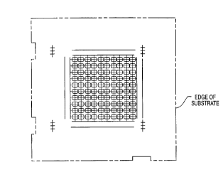
Provision is preferably made on the small-scaled plate 100 to facilitate alignment
(a) with the apparatuses that fabricate the small-scaled plate, and during assembly (b) with
liquid distribution systems and other processing or detection equipment. For many cases
mechanical alignment using three-pin registry is acceptable, and the edge alignment
20 locations specified in Figure 5 can be used. Although other alternatives can be used, the
preferred method is to grind first edge notch 105A, second edge notch 105B and third
edge notch 105C, for instance at the locations shown in Figure 5. The use of such
notches obviates the need to accurately machine all the edges of the small-scaled plate
100 and provides for a method of mechanically identifying the top and bottom of the plate
25 100. The location of the center of the cell patterns is defined in Figure 5 by the
intersection of lines B and C. The use of comparable notches in the m~nllf~cture of a
liquid distribution system with which the small-scaled plate operates allows equipment and
tool manufacturers to coordinate their designs.
In the illustrated small-scaled plate of Figure 5, examples of the distances
30 represented by Rl, R2, R3, Cm and Co are:
CA 022~1160 1998-10-02
wo 97/37755 ~ PCT~US97/0~841
- 13-
FOR~AT Rl R2 R3 Cm Co
lK 0.25 in 2.70 in 2.70 in 1.45 in 1.25 in
4K 0.25 in 3.70 in 3 70 in 1.95 in 1.75 in
IOOK 0.25 in 6.95 in 6.95 in 3.57 in 3.37 in
In some cases, optical alignment is preferable. The pr~f~ d location for the
optical fiducials, such as first fiducial 1 06A, second fiducial 1 06B and third fiducial 1 06C,
are illustrated in Figure 5.
For all of the above-described embodiments, the preferred support material will be
one that has shown itself susceptible to microfabrication methods, such as a
microfabrication method that can form channels having cross-sectional dimensionsbetween about 50 microns and about 250 microns. Such support materials include glass,
fused silica, quartz, silicon wafer or suitable plastics. Glass, quartz, silicon and plastic
support materials are preferably surface treated with a suitable treatment reagent such as a
siliconizing agent, which minimi7es the reactive sites on the material, including reactive
sites that bind to biological molecules such as proteins or nucleic acids. In embodiments
that require relatively densely packed electrical devices, a non-conducting support
material, such as a suitable glass, is preferred. Preferred glasses include borosilicate
glasses, low-alkali lime-silica glasses, vitreous silica (quartz) or other glasses of like
durability when subjected to a variety of chemicals. Borosilicate glasses, such as Corning
0211,1733,1737 or 7740 glasses, available from Corning Glass Co., Corning, NY, are
among the pl ~fel I ed glasses.
The reaction cells and horizontal channels and other structures of the small-scaled
plates can be made by the following procedure. A plate is coated sequentially on both
sides with, first, a thin chromium layer of about 500A thickness and, second, a gold film
about 2000 angstroms thick in known manner, as by evaporation or sputtering, to protect
the plate from subsequent etchants. A two micron layer of a photoresist, such asDynakem EPA of E~oechst-Celanese Corp., Bridgewater, NJ, is spun on and the
photoresist is exposed, either using a mask or using square or rectangular images, suitably
CA 022~1160 1998-10-02
W O 97/37755 PCT~US97/05841
- 14-
using the MRS 4500 panel stepper available from M:RS Technology, Inc., Acton, MA.
After development to form openings in the resist layer, and baking the resist to remove
the solvent, the gold layer in the openings is etched away using a standard etch of 4 grams
of potassium iodide and I gram of iodine (I2) in 25 ml of water. The underlying
5 chromium layer is then separately etched using an acid chromium etch, such as KTI
Chrome Etch of KTI Chemicals, Inc., Sunnyvale, CA. The plate is then etched in a bath,
such as an ultrasonic bath, of ~-HN03-H20 in a ratio by volume of 14:20:66. The use of
this etchant, for example in an ultrasonic bath, produces vertical sidewalls for the various
structures. Etching is continued until the desired etch depth is obtained. Vertical channels
10 are typically formed by laser ablation.
The gasket used to reversibly seal the plate to an instrument that functions with
the plate can be attached to the plate, leaving openings for the cells and other structures,
as needed. One method of att~ching the gasket is screen-printing. The printed gasket can
be made of silicone or another chemically-resistant, resilient material.
Alternatively, a multi-step compression-moldin;, process that utilizes
photolithography can be applied. First, the top surface of the plate, on which generally
cells and other structures have been forrned, is coated with a photoresist. Preferably, the
photoresist layer is about I mil in thickness. The photoresist layer is treated by standard
photolithography techniques to remove photoresist from those areas (the "gasket areas")
20 away from the apertures of the cells where gasket material is desired. A layer of a
flowable gasket material that can be cured to a resilient, elastomeric solid is applied. A
platen having a polished surface, for instance a polished glass surface, is placed above the
gasket material and pressure is applied to push the gasket material into the gasket areas
and substantially clear the gasket material from the photoresist-coated areas. The gasket
25 material is now cured. The photoresist is then dissolved, leaving the plate with a
patterned gasket. The gasket material is substantially cleared if it is sufficiently cleared to
allow the underlying photoresist to be dissolved.
In this process. the gasket material is any elastomeric material that is suitable for
use in the above-described compression molding technique, that is, when cured,
30 compatible with the chemistries that are to be practiced in the plate on which the gasket is
formed, and that is, when cured, resistant to the solvents used to remove the photoresist.
CA 022~1160 1998-10-02
Wo 97/37755 PCTrUSg7l0584
- 15 -
The gasket material is preferably silicone, such as RTV type silicone rubber (e.g.7 Silastic
J, RTV Silicone Rubber available from Dow Corning7 Midland7 Michigan). The
photoresist can be a film-type photoresist such that typically the structures on the plate
will not be filled during the compression-molding process or a liquid-type photoresist such
5 that the structures will temporarily be filled during the compression-molding process and
etched away at the completion of the process. In some instances, it is desirable to treat
the plate7 prior to the application of the photo-resist, with a primer for promoting the
adhesion ofthe gasket material7 such as 1200 RTV Prime Coat from Dow Corning7
Midland, Michigan. The plate can also be roughened to promote the adhesion of the
10 gasket material to the plate. For example7 5 micron roughness can be produced by
lapping. The platen is preferably treated with a release-promoter7 or a release promoter is
incorporated into the gasket materiaL as it is in Silastic J silicone rubber. The
compression-molding process can leave thin residues of gasket material at unwanted
locations. These residues are laser cut away from the plate or7 in some cases7 are
15 removed using a timed exposure to a solvent that dissolves the thin film of exposed gasket
material residue without having substantial effect on the thicker layer of gasket material
found at desired locations.
Another method of attaching the gasket is screen-printing. The printed gasket can
be made of silicone or another chemically-resistant, resilient material. Preferably7 the
20 gasket is made of a mixture of (a) a silicone rubber-forming material such as that available
under the Sylgard 184 brand from Dow Corning, Midland, Michigan or MDX4-4210T~'
also from Dow Corning and (b) an inert filler, such as the amorphous fumed silicon sold
as M-5 grade Cab-o-sil (Cabot Corp.7 Boston7 MA). Sylgard 184 and MDX4-4210 are
sold in two components. One component is an emulsion Cont~ining particles of silcone
25 rubber and a polymerization catalyst and the second component is a preparation of a bi-
valent monomer, which monomer serves to crosslink and thereby cure the silicone rubber.
Component one of MDX4-4210, i.e. the "elastomer component," is made up of
dimethylsiloxane polymer, reinforcing silica, and a platinum catalyst. Component two of
MDX4-4210, the "curing agent7" also contains dimethylsiloxane polymer, in addition to a
30 polymerization inhibitor7 and a siloxane crosslinker. The components are generally mixed
according to the manufacturer's recommendations. For example7 for MDX4-42107 ten
CA 022~1160 1998-10-02
W 097/3775~ PCTAUS97/OS841
- 16-
parts by weight of emulsion, i.e. elastomer, are mixed with one part of monomer solution,
i.e. curing agent.
As examples of the use of inert fillers, about 7. 5% by weight of M-5 grade Cab-o-
sil can be added to the Sylgard 184, or about 2-3% by weight of M-5 grade Cab-o-sil can
5 be added to the MDX4-4210. Filler can serve to thicken the pre-polymerized
composition to improve its screen printing properties. Gasket materials can generally be
cured at room temperature, or curing, can be accelerated with, for example, heat. Prior to
curing, the gasket-forming material is capable of flow, though generally viscous flow,
which flow is sufficient to facilitate the screen printing process. The gasket-forming
10 material is also sufficiently adhesive to adhere either to the plate to which it will be
applied or to an underlying first layer of gasket material.
In one version of the screen printing process, a first layer of gasket material is
printed onto the plate and then cured. After this first printing, a second layer of gasket
material is overlaid on the first, a smooth platen of appropriate shape (generally very flat)
15 is overlaid upon the printed gasket material so that a uniform weight is applied to the
printed gasket material (while taking precautions to prevent destructive adhesions of
gasket material to the platen such as described further below), and the gasket material is
cured. The use of two printings of gasket-forming material helps form a foundation of
gasket material prior to the smoothing process effected after the second printing and to
20 achieve the needed smoothness and uniform thickness of the sealing surface of the gasket.
To achieve this needed smoothness and uniform thickness, it is important to apply a
sufficiently uniform pressure to the gasket during a final curing process. This pressure
should be selected to be, for the particular gasket-applying process, sufficiently high to
create the needed uniformity during the curing process, but not so high as to overly
25 compress cured portions of gasket material such that upon release of the pressure these
portions re-expand and create a non-uniform seal thickness. A single print process can
also be used, and such a single print process is generally preferred since it is simpler and
more readily applied to a production process. ln a single print process, which is described
further below, a platen is applied directly after the first (and only) printing of gasket
30 material, and prevented from settling down too far or too unevenly by mechanical stops.
Preferably, the width of each print feature on the screen is uniform, as width non-
uniformities increase the probability of a thickness non-uniformity at the end of the
CA 022~1160 1998-10-02
W O 97/37755 PCTrUS97/05841
- 17-
process. Figure 6B shows an illustrative print screen pattern, wherein gasket material is
applied between the closely spaced (here, for example 6 mils) lines. After printing and
processing, the applied gasket patterns are broadened. For example, in applications using
the two-print process and 6 mil wide pattern on the print screen, an 18 mils wide pattern
5 has been produced. In Figure 6A, the fifty figure eight patterns outlined in dark lines
represent the gasket about one hundred reaction wells on a reaction cell plate, with the
individual wells (not shown) located within the two openings in the illustrated figure eight
patterns. In Figure 6B is illustrated a print screen pattern used to generate one of the
figure eight patterns. In another embodiment, each individual reaction well has an O-
10 shaped gasket pattern about it. This latter embodiment avoids the gasket boundary sharedby two reaction wells in the pattern of Figures 6A and 6B. This shared boundary can be
more susceptible to non-uniformities than the other boundaries of the pattern. The
dimensions illustrated in Figure 6B are in inches.
strative two-print protocol: The plate, in this case a 2 X 2 inch glass plate, is
15 cleaned in a Class 10,000 or, preferably, cleaner cleanroom environment. The plate is
inspected under a microscope for lint and deposits. These are removed with tweezers and
by a stream of propanol or other solvent. The plate is wiped with a lint-free cloth and
vapor cleaned with ethanol. After drying, the plate can be stored in a container. The
gasket forming material is prepared by degassing the material (e.g., M:DX 4-421020 under vacuum. Care is taken to align the register between the plate and the print screen.
The plate can be aligned with three-pin registry with the notches indicated at the edges of
the plate illustrated in Figure 6A. The gasket pattern is then printed on the plate, the plate
is isolated in a clean container, and the gasket is cured by placing the container in a 70 C
oven for 4 hours. Then, the same gasket pattern is overlaid on the first. A thin,
25 preferably transparent, plastic film (for example, a 3 mils thick polyester film) coated with
a mold.release (for example, 3~/0 wt/v aqueous sodium lauryl sulfate) is layered on top of
the printed gasket pattern. Then, a flat, smooth platen is set on top of the release film to
evenly apply a weight, for example 21/2 Ibs., onto the printed gasket pattern.
Alternatively, instead of using the film, a mold release agent such as a surfactant can be
30 directly applied to the platen to assure that it does not adhere to the gasket material. The
gasket is then cured while the evenly distributed weight is applied. For testing, the release
CA 022~1160 1998-10-02
Wo 97/37755 PCT/US97/0584
- l8 -
film is carefully removed, and the gasket examined under a microscope for defects. A
clean, smooth plate can be placed on top of the gasket, and a clamping pressure of, for
example, 20 Ibs. is applied to the gasket pattern of Figure 6A. In a successful print, a
contacting interface for each seal segment should be visible. The gasket should be stored
5 in contact with a release film.
Illustrative single-print protocc~l: The plate is prepared as described above, and a
gasket is printed on the plate as described above, taking special care that the gasket-
forming material is evenly applied by the print screen. lmmediately after this single
printing, a transparent, plastic film, which is coated with a release coating, is layered over
10 the printed pattern, and a smooth, flat platen is positioned over the film and the underlying
printed pattern. The platen is impressed upon the pattern until it is met by mechanical
stops that hold the platen at a uniform height above the plate. The gasket is then cured
while the platen is in place. The gasket can be tested and stored as described above.
The screen used in the printing can be formed for example using conventional
15 photolithographic means. Thus, it can be the same type of screen as those used in the
m~nllf~c.ture of printed circuit boards. The screen is for example woven from 0.9 mil
stainless steel wire. The weave pattern is preferably oriented a~ lbout a 45 degree angle
from the printing (squeegee) direction. The photolithographlc emulsion on which the
pattern is made in can be, for example, 2.5 mils thick. With the 6 mil screen pattern width
20 illustrated in Figure 6B and the 2.5 mil screen pattern depth, the gasket width after curing
is typically about 18 mil and the thickness of the seal is typically about 1.3 mils. In
printings using MlDX 4-4210, a typical product gasket has a hardness of about 65durometer.
The width and thickness of the gasket can be varied by, for example, varying the25 dimensions of the screen pattern, varying the size of emulsion particles in the polymeric
component of the gasket-forming material, varying the weight applied in the curing
process, and adding additives to the gasket-forming material such as an inert filler.
It should be recognized that the gasket-forming process, while preferably app}ied
to the flat plates contemplated in the preferred embodiments of the liquid distribution
30 system, can also be applied to any other surfaces to which a complementary surface can
be sealed via the gasket. Generally, such other surfaces will be sufficiently smooth so as
to facilitate printing of the gasket and sealing to the complementary surface.
CA 022~1160 1998-10-02
W O 97137755 PCTAUS9710S841
- 19-
While this invention has been described with an emphasis upon plerelled
embo~im~nt~, it will be obvious to those of ordinary skill in the art that variations in the
preferred devices and methods may be used and that it is intended that the invention may
be practiced otherwise than as specifically described herein. Accordingly, this invention
S includes all modifications encompassed within the spirit and scope of the invention as
defined by the claims that follow.