Note: Descriptions are shown in the official language in which they were submitted.
CA 022~1219 1998-10-07
W O 98/39801 PCT~B98/0051
THIN FILM FERROELECTRIC CAPACITORS HAVING IMPROVED
MEMORY RETENTION THROUGH THE USE OF ESSENTIALLY SMOOTH
BOTTOM E~ECTRODE STRUCTURES
BACKGROUND OF THE INVE~NTION
1. Field of the Invention
The present invention pertains to method and apparatus involving thin film
ferroelectrics for use in integrated circuits. More particularly, a smooth bottom
electrode structure adjacent a ferroelectric thin film layered superlattice material
improves the memory retention characteristics of a ferroelectric capacitor through
less imprint and longer memory retention time.
2. Sfatement of the Problem
Thin film ferroelectric materials are used in a variety of nonvolatile random
access memory devices. For example, U.S. patent number 5,600,587 issued to
Koike teaches a ferroelectric nonvolatile random access memory using memory
cells consisting of a ferroelectric capacitor and a switching transistor. U.S. patent
number 5,495,438 issued to Omura teaches a ferroelectric memory that is formed
of ferroelectric capacitors connected in parallel. The capacitors have ferroelectric
materials of different coercive field values and, consequently, can use or storemulti-value data. U.S. patent number 5,592,409 issued to Nishimura et al teachesa nonvolatile memory including a ferroelectric layer that is polarized by the
impressed voltage between two gates. The polarization or memory storage state
is read as a high or low current flow across the ferroelectric layer, which permits
nondestructive readout. U.S. patent number 5,539,279 issued to Takeuchi et al
teaches a high speed one transistor-one capacitor ferroelectric memory that
switches between two modes of operation including a dynamic random access
memory ("DRAM") mode and a ferroelectric random access memory ("FERAM")
mode.
FIG. 1 depicts an ideal polarization hysteresis curve 100 for ferroelectric thinfilms. Side 102 of curve 100 is produced by measuring the charge on a
ferroelectric capacitor while changing the applied field E from a positive value to a
negative value. Side 104 of curve 100 is produced by measuring the charge on theferroelectric capacitor while changing the applied field E from a negative value to
--1--
CA 022~1219 1998-10-07
W O 98/39801 PCT/IB98100515
a positive value. The points -Ec and Ec are conventionally referred to as the
coercive field that is required to bring poiarization P to zero. Similarly, the remanent
polarization Pr or -Pr is the polarization in the ferroelectric material at a zero field
value. The Pr and -Pr values i~eally have the same magnitude, but the values are5 most often different in practice. Thus, polarization measured as 2Pr is calculated
by adding the absolute values of the actual Pr and -Pr values even though these
values may differ in magnitude. The spontaneous polarization values Ps and -Ps
are measured by extrapolating a linear distal end of the hysteresis loop, e.g., end
106, to intersect the polarization axis. In an ideal ferroelectric, Ps equals Pr, but
10 these values differ in actual ferroelectrics due to linear dielectric and nonlinear
ferroelectric behavior. A large, boxy, substantially rectangular central region 108
shows suitability for use as a memory by its wide separation between curves 102
and 104 with respect to both coercive field and polarization.
Presently available ferroelectric materials depart from the ideal hysteresis
15 shown in FIG. 1. Researchers have investigated materials for use in integrated
ferroelectric devices since the 1970's, but these investigations have not yet been
commercially successful due to the development of materials that depart from theideal hysteresis. For example, U.S. patent number 3,939,292 issued to Rohrer
reports that early studies of ferroelectric materials for use in ferroelectric memories
20 were performed on phase lll potassium nitrate. In practice, it turned out that
potassium nitrate materials had such low polarizabilities and were so badly afflicted
by fatigue and imprint that the materials were practically useless in microelectronic
memories. It is nearly impossible to find ferroelectrics that meet commercial
requirements. The best materials for integrated ferroelectric devices are switched
2~ using a coercive field that can be obtained from conventional integrated circuit
operating voltages, i.e., three to five volts ("V"). The materials should have a very
high polarization, e.g., one exceeding twelve to fifteen microCoulombs per square
centimeter (",uC/cm2 ) determined as 2Pr, to permit the construction of memorieshaving sufficient densities. Polarization fatigue should be very low or nonexistent.
30 Furthermore, the ferroelectric material should not imprint, i.e., the hysteresis curve
should not shift to favor a positive or negative coercive field.
CA 022~1219 1998-10-07
W O 98/39801 PCT/LB98/00515
FIG. 2 depicts the effects of environmental stress on hysteresis curve 100.
Curve 200 shows the effect of fatigue on curve 100. Fatigue reduces the
separation between curves 102 and 104 defining centrai region 108. Central region
108 progressively becomes smaller and smaller with additional fatigue. This
5 change in separation is due to the creation of point charge defects arising in the
ferroelectric material as a consequence of polarization switching together with the
associated screening effect of the charge defects on the applied field. Thus,
fatigue causes the ferroelectric material to wear out over time due to repeated
polarization switching.
U.S. patent number 5,519,234 issued to Araujo et al. teaches that the fatigue
problem of curve 200 is substantially overcome by the use of layered superlattice
materials, such as the "layered perovskite-like" materials described in Smolenskii
et al "Ferroelectrics and Related Materials," Gordon and Breach (1984). The
layered superlattice materials are capable of providing a thin film ferroelectric
15 material wherein the polarization state may be switched up to at least 109 times with
less than thirty percent fatigue. This level of fatigue endurance provides a
significant advance in the art because it is at least about three orders of magnitude
better than the fatigue endurance of other ferroelectrics, e.g., lead zirconium
titanate ("PZT") or lead lanthanum zirconium titanate ("PLZT"). Prior layered
20 superlattice material work has been done primarily with the use of a PVTi bottom
electrode and layered superlattice material films on the order of 1800 A thick. The
titanium is used as an adhesion layer to prevent peeling of the electrode from the
substrate .
According to section 15.3 of the Smolenskii book, the layered perovskite-like
25 materials or layered superlattice materials can be classified under three general
types:
(A) compounds having the formula Am ,Bi2MmO3m+3, where A = Bi3+, Ba2+, Sr2+,
Ca2+, Pb2+, K+, Na+ and other ions of comparable size, and M = Ti4+, Nb5+,
Tas+, Mo6+, W6+, Fe3+ and other ions that occupy oxygen octahedra;
30 (B) compounds having the formula Am+,MmO3m+" including compounds such as
strontium titanates Sr2TiO4, Sr3Ti207 and Sr4Ti30,0; and
CA 022~1219 1998-10-07
W 098/39801 PCT ~ 98/0051S
(C) compounds having the formula AmMmO3m,2, including compounds such as
Sr2Nb2O7, La2Ti2O7, SrsTiNb4O17~ and Sr6Ti2Nb4O20
Smolenskii pointed out that the perovskite-like layers may have different
thicknesses, depending on the value of m, and that the perovskite AMO3 is in
5 principal the limiting example of any type of layered perovskite-like structure with
m = infinity. Smolenskii also noted that if the layer with minimum thickness (m=1)
is denoted by P and the bismuth-oxygen layer is denoted by B, then the type I
compounds may be described as .. BPmi3Pm.. Further Smolenskii noted that if m
is a fractional number then the lattice contains perovskite-like layers of various
10 thicknesses, and that all the known type I compounds are ferroelectrics.
Despite the tremendous improvements in low fatigue ferroelectrics
attributable to layered superlattice materials, there remains an imprint problem that
is typified by curve 202 of FIG. 2. Curve 202 shows that environmental stresses
can imprint curve 100 by shifting it to the right or left. This imprinting occurs when
15 the ferroelectric material is subjected to repetitive unidirectional voltage pulses.
Some imprinting also occurs as a result of normal hysteresis switching. The
ferroelectric material retains a residual polarization or bias that shifts sides 102 and
104 in a positive or negative direction with respect to the applied field. Thus, curve
202 has been shifted in a positive direction 204 by repeated negative pulsing of a
20 ferroelectric capacitor. A shift in the opposite direction could also occur due
repetitive pulsing by opposite voltage. This type of pulsing represents what
happens to the ferroelectric materials as a consequence of repeated unidirectional
voltage cycling, such as the sense operations in ~ERAMs. Imprint can be so
severe that the ferroelectric material can no longer retain a polarization state25 corresponding to a logical 1 or 0 value.
U.S. patent number 5,592,410 issued to Verhaeghe refers to the ferroelectric
imprint phenomenon as 'compensation.' The '410 patent teaches that the imprint
problem can be reversed by pulsing voltage during the write cycle to return the
hysteresis loop towards the unimprinted position of curve 100, as compared to
30 curve 202. Thus, the imprint problem is reversed by special write operations in
which the pulsed voltage is opposite the switching voltage. Still, the recommended
voltage pulsing does not address the entire probiem because the imprint
.
CA 022~l2l9 l998-l0-07
W O 98/39801 PCT~B98/00515
phenomenon is a partially irreversible one. The observed imprinting reflects
corresponding changes in microstructure of the ferroelectric crystal, e.g., the
creation of point charge defects with associated trapping of polarized crystal
domains. These changes in microstructure are not all reversible.
FIG. 3 depicts the deleterious effects of fatigue and imprinting on
ferroelectric memory read/write control operations. Memory control logic circuits
require a minimum polarization separation window, which is represented by shadedregion 300. Region 300 must be large enough to produce a sufficient read-out
charge for memory operations, e.g., for the operation of memory sense amplifier
10 circuits. An initial 2Pr separation window 302 declines over the lifetime of the
ferroelectric memory device along tracks 304 and 306 until, after about ten years
or so of constant normal use, the separation between tracks 304 and 306 is too
small for conducting memory operations. This lifetime of normal use follows stress
time line 308. Curve 310 is a polarization hysteresis curve from the same material
15 that produced curve 100, but is measured on decline at a point in time along tracks
304 and 306. The remanent polarization values Rms and Rmn correspond to +Pr
and -Pr for the fatigued and imprinted material. Rms and Rmn are defined as
remanent polarization at zero field in the fatigued hysteresis curve 310. Arrow 312
shows a quantity of positive polarization retention loss, which is primarily due to
20 fatigue. Arrow 314 shows a quantity of negative polarization imprint loss, which is
primarily caused by imprint shifting of curve 312 relative to curve 100. Arrow 316
shows a quantity of voltage center shifting of curve 312 relative to curve 100. This
voltage center shifting indicates imprinting of the ferroelectric material.
There remains a need for ferroelectric thin film capacitors that resist fatigue
25 well, have long memory retention times, and are substantially free of the imprint
problem .
SOLUTION
It has been discovered that the imprint phenomenon represented as curve
202 in FIG. 2 is affected by surface irregularities on the ferroelectric film, e.g.,
30 those corresponding to hillocks on the bottom electrode in a thin film ferroelectric
capacitor device or similar surface irregularities on the top of the ferroelectric film
In particular, the prior art PVTi bottom electrodes form sharp hillocks that are
CA 022~1219 1998-10-07
W O 98/3g801 PCT~B98100S15
especialiy prone to increase the amount of imprinting. Thus, ferroelectric capacitors
having electrodes with sharp irregularities offer inferior electronic performance in
integrated memories.
The present invention overcomes the problems outlined above by providing
5 an essentially smooth or hillock-free bottom electrode for use in combination with
layered superlaKice materials. The ferroelectric materials are specially processed
in deposition to present a similarly smooth surface for receipt of a top electrode.
The layered superlattice materials resist fatigue well and their conformity to the
smooth bottom electrode improves their imprint performance in integrated
10 ferroelectric memories, such as FERAMs.
The smooth electrodes also permit the use of increasingly thinner films of
layered superlattice materials without shorting of the ferroelectric capacitors. The
thin films show a surprising improvement in their memory retention windows
because memory retention windows in the thinner materials can have a greater
15 magnitude than exists in comparable thicker materials. One would expect just the
opposite effect because a greater number of oriented ferroelectric domains in the
thicker materials should provide a greater cumulative polarization effect, but this
greater cumulative polarization effect is not observed in practice. Thus, the use of
smooth electrodes and thin films permits the construction of much better
20 ferroelectric memories.
A thin film ferroelectric capacitor according to the present invention includes
a bottom electrode having a first smooth surface, a ferroelectric thin film layered
superlattice material, and a top electrode having a second smooth surface. The
most preferred layered superlattice materials are strontium bismuth tantalate and
25 strontium bismuth niobium tantalate. The ferroelectric thin film layered superlattice
material contacts the smooth surfaces of the electrodes and has a thickness
ranging from 500 A to 2300 ~. A smooth surface on one of the electrodes is hereby
defined as one in which all surface irregularity features protruding towards the thin
film ferroelectric layered superlaKice material protrude a distance less than twenty
30 percent of the thickness in the ferroelectric thin film layered superlattice material
thickness. It is also preferred that substantially all of the surface irregularities on
the smooth electrode are rounded and essentially free of acute angles. Another
CA 022~1219 1998-10-07
W O 98/39801 PCT~B98/00515
way of defining a smooth surface is that the surface is smoother, i.e., having
surface irregularities that are less sharp, less tall, and less numerous, than the
surface irregularities of a comparable 2000 ~ / 200 A thick Pt / Ti stacked electrode
deposited on silicon which has been annealed while exposed to oxygen at 500 ~C
to 800 ~C for one hour.
Ferroelectric thin film layered superlattice materials for use in the invention
typically have thicknesses ranging from 500 A to 2300 A. Thicknesses above this
range are also useful, though they are seldom needed. A more preferred range of
layered superlattice material thickness is from 500 A to 1100 A. This range is even
10 more preferably from 500 ~ to 1000 ~, and is most preferably from 500 A to 800 ~.
The prior art does not show layered superlattice materials having these small
thicknesses which are less than about 1300 ~.
Ferroelectric capacitors of the invention demonstrate superior electronic
performance. For example, the ferroelectric thin film layered superlattice material
15 is capable of providing a 3 V polarization or charge separation window of at least
7 ~C/cm2 after being fatigued by 10'~ cycles of 6 V square wave switching at 125~C. These 6V switching pulses are very high, as compared to normal integrated
circuit operating voltages and, consequently, tend to accelerate fatigue. The 7
,uc/cm2 separation window is sufficient for proper interaction with conventional20 integrated memory control logic circuits. The separation window increases as film
thickness decreases down to about 500 A Layered superlattice material films
thinner than about 500 A crystallize differently and show porosity along grain or
domain boundaries, which makes them unsuitable for use in ferroelectric
capacitors.
Another aspect of superior electronic performance in the ferroelectric thin
film layered superlattice materials according to the invention is superior resistance
to imprinting. The ferroelectric thin film layered superlattice materials are also
capable of demonstrating a hysteresis shift of less than 0.11 V corresponding to the
3 V polarization separation window after 1 o10 cycles of 6 V square wave switching,
30 as described above.
Yet another aspect of superior electronic performance is the development
of ultra thin ferroelectric layered superlattice material films that are essentially
CA 022~1219 1998-10-07
W O98139801 PCTIIB9810051S
fatigue free. The use of smooth electrodes permits the use of ferroelectric thin films
having less than about 2% of 2Pr degradation after being switched 10'~ cycles
using a 1.5 v triangular wave at 10,000 Hz. This exceptional ferroelectric
performance comes from ultra thin films, e.g., those ranging from 500A to 800A in
5 thickness.
In a preferred embodiment, the bottom electrode includes a platinum layer
deposited on a titanium dioxide layer.
In another preferred embodiment, the bottom electrode includes a platinum
layer deposited on a metal nitride, e.g., TiN, diffusion barrier layer on a titanium
10 adhesion layer.
In less preferred embodiments, the bottom electrode includes a platinum
layer on a titanium adhesion layer. These embodiments are less preferred becauseadditional processing is reauired to provide a bottom electrode that is essentially
free of sharp hillocks. A smooth electrode has a PVTi intermetallic barrier region.
15 The metals are annealed at 600 ~C to 800 ~C for 30 minutes to 2 hours under atemporary capping layer of metal oxide, which is subsequently removed by an HF
enchant and replaced by a second platinum layer. Alternatively, a layered
superlattice material may be used as a thermal stress.buffer layer interposed
between the Pt / Ti stacked bottom electrode and the underlying substrate, e.g., a
20 silicon wafer. The top electrode is preferably platinum.
The process of making the ferroelectric capacitors includes careful control
of thermal process conditions. A smooth bottom electrode is formed wherein
substantially all surface irregularity features on a bottom electrode are rounded and
essentially free of acute angles. This smoothness derives from a proper selection
25 of materials and anneal temperatures. For example, the need for smoothness
requires a platinum on titanium dioxide electrode to be annealed under oxygen ata temperature of not more than almost exactly 450 ~C.
A liquid precursor is deposited on the bottom electrode to provide a
precursor film. The precursor film is capable of yielding a ferroelectric layered
30 superlattice material upon drying and annealing of the precursor film. Drying of the
precursor film is done at a temperature less than 400 ~C to provide a dried
precursor residue. The dried precursor residue is soft baked using rapid thermal
-8 -
. . , _ . . . . .. .
CA 022~1219 1998-10-07
W O 98/39801 PCT~B98/00515
processing ("RTP") at an RTP temperature ranging from 525 ~C to 725 ~C for a
period of time ranging from thirty seconds to five minutes. The RTP temperature
more preferably ranges from 625 ~C to 650 ~C, and is most preferably 650 ~C,
which is the highest temperature that consistently produces a smooth upper surface
5 on the resultant soft baked precursor residue. The soft baked precursor residue is
annealed in a diffusion furnace under oxygen at an anneal temperature ranging
from 500 ~C to 650 ~C. The anneal temperature more preferably ranges from 520
~C to 560 ~C, and is most preferably 550 ~C, which is just barely sufficient to
crystallize the ferroelectric layered superlattice material from the soft baked
10 precursor residue.
Other features, objects, and advantages will become apparent to those
skilled in the art upon reading the detailed description below in combination with the
accompanying drawings.
BRIEF DESCRIPTION OF THE DRAWINGS
FIGURE 1 depicts an idealized conventional ferroelectric polarization
hysteresis curve with reference to conventional nomenclature used to describe
aspects of the curve;
FIG. 2 depicts the idealized FIG. 1 curve adjacent other curves
20 demonstrating polarization fatigue and polarization imprint problems;
FIG. 3 depicts a schematic representation of the probtems that memory
control circuitry faces when the ferroelectric materials in ferroelectric memories
degrades due to fatigue and imprint problems;
FIG. 4 depicts a ferroelectric capacitor having essentially smooth electrodes
25 according to the present invention;
FIG. 5 depicts a circuit diagram of an integrated circuit memory which is a
preferred use of the FIG. 4 ferroelectric capacitor;
FIG. 6 depicts a circuit diagram of an individual integrated circuit non-volatile
memory cell such as may be used in the memory of FIG. 5 and utilizing the
30 FIG. 4 ferroelectriccapacitor;
CA 022~1219 1998-10-07
W 098139801 PCT~B98/00515
FIG. 7 depicts a layered construction showing how individual memory cells
may be implemented in an integrated circuit memory corresponding to FIGS. 5 and
6;
FIG. 8 depicts a schematic process diagram for use in making a memory
5 cell corresponding to the FIG. 7 layered construction;
FIG. 9 depicts a process for testing ferroelectric fatigue and imprint together
with memory retention over time;
FIG. 10 depicts a comparison of an imprint indicator among several
ferroelectric capacitors that were prepared according to different process
10 conditions;
FIG. 11 depicts a polarization hysteresis curve obtained from an ultra thin
ferroelectric capacitor that was produced according to the present invention;
FIG. 12 depicts a polarization fatigue endurance curve that was obtained
from the sample used in the hysteresis measurement of FIG. 11;
FIG. 13 depicts a scanning electron microscopic photograph of a rough
bottom eiectrode that is undesirable for use in the present invention; and
FIG. 14 depicts a transmission electron microscopic photograph of a thin
film ferroelectric layered superlattice material on a smooth bottom electrode for use
according to the present invention.
DETAILED DESCRIPTION OF THE PREFERRED EMBODIMENT
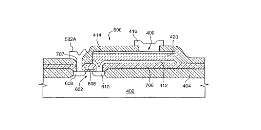
FIG. 4 depicts a preferred ferroelectric capacitor 400 according to the
invention. A conventional wafer 402 supports ferroelectric capacitor 400, and ispreferably a silicon wafer, but may also be any other conventional material including
25 at least indium antimonide, magnesium oxide, strontium titanate, sapphire, quartz
ruby, gallium arsenide, and combinations of these materials. A first isolation layer
404 of silicon dioxide, e.g., at least about 2000 A thick, is preferably formed atop
a silicon wafer 402. An adhesion layer 406 is made of titanium dioxide, which isalso preferably about 1000 A thick, followed by a 3000 A thick platinum layer 410.
30 A diffusion barrier layer 408 of about 1500 A thick titanium nitride is optionally
formed, atop the adhesion layer 406. Where the diffusion barrier layer 408 is used,
-10-
.
CA 022~1219 1998-10-07
W O98/39801 PCT~B98/00515
adhesion layer 406 may comprise a 200 A thickness of sputtered titanium, and
ptatinum layer 410 may be 1500 A thick.
Layers 406, 408, and 410 comprise bottom electrode 412, which presents
a first smooth upper surface 414 having a plurality of surface irregularities, e.g.,
5 irregularities 416 and 418. A surface irregularity is hereby defined as a structural
feature on the surface of an electrode that breaks what would, otherwise, be a
smooth and uninterrupted flow of the electrode according to an intended contour.Examples of surface features include sharp or acute hillocks, small rounded
mounds, and small rounded pits, in what is intended to be an essentially planar
10 electrode surface. The thin film surface features or irregularities are visible at high
magnification under scanning electron microscopic observation. The surface
irregularities 416 and 418 are all rounded and essentially free of acute angles of the
type that may be observed in hillocks on conventional Pt/Ti electrodes.
Alternative smooth electrode structures may be substituted for the bottom
15 electrode 412 that is shown in FIG. 4. These alternative smooth electrode
structures include Pt / Ti and Pt / SiO2 stacked electrodes. Pt / Ti electrodes are
generally undesirable because they are too rough unless they are made by the
special processes described in copending applications serial numbers 08/427,897
and 08/473,432. Any smooth electrode may be used as bottom electrode 412, and
20 it will be understood that additional layers or fewer layers may be added to the
example structure shown in FIG. 4, as required for whatever reason so long as the
bottom electrode remains essentially smooth. Smoothness is especially needed
for preventing spikes on the bottom electrode 412 from causing shorts through
ferroelectric capacitor 400. Electrode smoothness also prevents surface
25 irregularities from causing point charge or line defects in the thin film ferroelectric
layered superlattice material layer 420.
A thin film ferroelectric layered superlattice material layer 420 contacts firstsmooth surface 414. Substantially none of the surface irregularities 416 and 418on first smooth surface 414 protrude vertically towards ferroelectric layer 420 a
30 distance greater than twenty percent of the vertical thickness in layer 414. It is
even more preferable that these surface irregularities protrude less than fourteen
percent.
-1 1 -
CA 022~1219 1998-10-07
W O 98/39801 PCT~B98100515
A 2000 A thick platinum top electrode 422 presents a second smooth
surface 424 having a plurality of associated surface irregularities, e.g., irregularity
426. The surface irregularities 426 are all rounded and essentially free of acute
angles of the type that may be observed in the hillocks of a conventional Pt / Ti
5 stacked electrode. Substantially none of the surface features 416 and 418 on first
smooth surface 414 protrude vertically towards ferroelectric layer 420 a distance
greater than twenty percent of the vertical thickness in layer 414. Ferroelectric
layer 420 conforms to first surface 414 and second surface 428 at the
corresponding contact interfaces between ferroelectric layer 420, platinum layer10 410 and top electrode 422.
There are two main reasons why the surface irregularities 416, 418, and 426
do not protrude into ferroelectric layer 420 a distance greater than twenty percent
of the thickness in ferroelectric layer 420. The first reason involves breakdownvoltage. The layered superlattice materials that have been studied thus far have15 breakdown voltages of about one MV/cm, i.e., from 0.9 MV to 1.1 MV. Thus, about
100 A of layered superlattice material are needed to withstand 1 V without
breakdown. It follows that two irregularities could be superposed over one another
between the electrodes, e.g., as surface irregularity 426 in substantial alignment
with surface irregularity 416. Complete polarization of ferroelectric layer 420 cannot
20 happen if breakdown occurs. Thus, at least 150 A of layered superlattice material
are needed to withstand a 1.5 V potential between electrodes 412 and 422. A 500
A thick ferroelectric layer 420 that is designed to operate at 3 V requires a 300 A
thickness. Thus, a hillock can protrude only 200 A into ferroelectric layer 420. The
200 A equals forty percent (200/500 = 40%) of the ~00 A thickness in layer 420.
25 About half of this value, i.e., twenty percent, is required for each electrode because
the surface irregularities may be in vertical alignment across the respective
electrodes.
The second reason involves a need to avoid imprinting ferroelectric layer
420. It has been determined from qualitative scanning electron microscopic data
30 that surface irregularities of larger height have a greater effect in imprinting
ferroelectric layers, such as ferroe!ectric layer 420, which contact electrodes having
these large surface irregularities. Thus, the requirement that surface irregularities
-12-
. . .
CA 022~l2l9 l998-l0-07
W O 98/39801 PCT~B98/00515
on each electrode protrude less than twenty percent into ferroelectric tayer 420 is
more preferably less than fourteen percent and even more preferably less than
seven percent, though it is difficult to make seven percent electrodes for use with
500 A and 600 ~ thick ferroelectric layers 420.
Ferroelectric capacitor device 400 forms part of an integrated memory circuit
in the intended environment of use. Those skilled in the art understand that
ferroelectric capacitor devices have additional uses including use as ferroelectric
transistor gates and logic circuits.
FIG. 5 is a block diagram illustrating an exemplary integrated circuit memory
10 500 in which ferroelectric switching capacitors or high dielectric constant capacitors
made with the materials of the invention are utilized. For simplicity, the
embodiment shown is for a 16 kilo bit ("16 K") DRAM; however the material may beutilized in a wide variety of sizes and types of memories, both volatile and non-
volatile. In the 16K embodiment shown, there are seven address input lines 502
15 which connect to a row address register 504 and a column address register 506.
The row address register 504 is connected to row decoder 508 via seven lines 510,
and the column address register 506 is connected to a column decoder/data input
output multiplexer 512 via seven lines 514. The row decoder 508 is connected to
a 128 X 128 memory cell array 516 via 128 lines 518, and the column decoder/data20 input output multiplexer 512 is connected to the sense amplifiers 520 and memory
cell array 516 via 128 lines 522. A RAS signal line 524 is connected to the row
address register 504, row decoder 508, and column decoder/data inpuVoutput
multiplexer 512, while a CAS signal line 526 is connected to the column address
register 506 and column decoderldata input output multiplexer 512. (In the
25 discussion herein, a ~ indicates the inverse of a signal.) An inpuVoutput data line
528 is connected to the column decoder/data input output multiplexer 512. Memorycell array 516 contains 128 x 128 = 16,384 memory cells, which is conventionallydesignated as 16K. These cells are ferroelectric switching capacitor-based cellsaccording to the present invention.
FIG. 6 depicts a ferroelectric capacitor-based switching cell 600. Cell 600
includes two electrically interconnected electrical devices, namely, a transistor 602
and a ferroelectric switching capacitor 400. The gate 606 of transistor 602 is
-13-
CA 022~1219 1998-10-07
W O98/39801 rCT/lB98/0051
connected to line 518A, which is one of the lines 518 (see FIG. 5) which are
generally called "word lines". Source/drain 608 of transistor 602 is connected to line
522A, which is one of lines 522 that are generally called "bit lines". The othersource/drain 610 of transistor 602 is connected to bottom electrode 412 of
5 switching capacitor 400. The top electrode 422 of switching capacitor 400 is
connected to line 616 which is connected to a reference voltage Vref.
Cell 600 may be fabricated as an integrated circuit FERAM, as shown in FIG.
7. The individual elements just described in connection with FiG. 6 are labeled with
the same numbers in FIG. 6. As shown in FIG. 7, memory cell 600 includes a thin
10 film ferroelectric layer 420. Wafer 402 is doped to provide source/drain regions
608 and 610. Layer 706 is an additional isolation layer that is preferably made of
spin-on glass, or other phosphorous-doped or non-doped silicon dioxide. Bottom
electrode 412 is constructed as described in the discussion of FIG. 4. Bit line 522A
is preferably made of platinum, or aluminum.
The operation of the memory in FIGS. 5 through 7 is as follows. Row
address signals Ao through A6 (see FIG. 5) and column address signals A7 throughAl3 placed on lines 502 are multiplexed by address registers 524 and 526 utilizing
the RAS- and CAS signals, and passed to the row decoder 508 and column
decoder/data inpuVoutput multiplexer 512, respectively. The row decoder 508
20 places a high signal on the one of the wordlines 518 that is addressed. The column
decoder/data input output multiplexer 518 either places the data signal which isinput on line 528 on the one of the bit lines 522 corresponding to the column
address, or outputs on the data line 528 the signal on the one of the bit lines 522
corresponding to the column address, depending on whether the function is a write
25 or read function. As is known in the art, the read function is triggered when the
RAS signal precedes the CAS signal, and the write function is triggered when theCAS- signal comes before the RAS- signal. The transistors 602 in the respective
cells 600 connected to the word line that is high turn on, permitting the data signal
on the bit line 522A to be read into the capacitor 400 or the signal on the capacitor
30 400 to be output on the bit line 522A, depending on whether the read or writefunction is implemented. As is well-known in the art, the sense amplifiers 520 are
located along lines 522 to amplify the signals on the lines. Other logic required or
-14-
CA 022~l2l9 l998-l0-07
W O 98/39801 PCT~B98/OOS15
useful to carry out the functions outlined above as well as other known memory
functions is also included in the memory 500, but is not shown or discussed as it
is not directly applicable to the invention.
As outlined above, the RAS and CAS lines 524 and 526; registers 504 and
5 506; the decoders 508 and 510; and the transistor 602 comprise an information
write means 618 (see FIG. 6) for placing the memory cell 600 in a first memory
state or a second memory state depending upon information input to the memory
on data line 528. The first memory cell state corresponds to layer 420 of
ferroelectric material being in a first polarization state, and the second memory cell
10 state corresponds to the layer 420 being in a second polarization state. These
components plus sense ampiifiers 520 comprise an information read means 620
for sensing the state of memory cell 600 and providing an electrical signal
corresponding to the state. The necessity of sensing the polarization state of thin
film ferroelectric layer 420 causes information read means to subject thin film
15 ferroelectric layer 420 to repeat unidirectional voltage pulses.
Thin film ferroelectric layer 420 is preferably formed using a liquid depositionprocess, such as the process described in U.S. patent number 5,423,2$5. In this
process, metal alkoxycarboxylates are mixed in relative proportions that are
designed to yield a corresponding metal oxide of a desired stoichiometry. A liquid
20 film of the precursor solution is dried and annealed to yield the desired metal oxide.
FIG. 8 depicts a schematic process diagram of process P800 for fabricating
memory cell 600 of the present invention. In step P802, wafer 402 is made ready
by conventional means to receive thin film ferroelectric layer 420. Accordingly, a
silicon wafer 402 may be heated in an oxygen diffusion furnace to grow oxide layer
25 404. A contact hole 707 may be formed through oxide layer 404 by ion etching or
other techniques to expose wafer 402, which is then n or p-doped by conventionalmeans to provide source/drain regions 608 and 610. Transistor gate 606 is formedby conventional means. Isolation layer 706 may be deposited as spin-on glass or
other phosphorous-doped or non-doped silicon dioxide by conventional chemical
30 vapor deposition.
Bottom electrode 412 is formed in step P804. Titanium dioxide is formed by
first sputtering titanium to a thickness ranging from 500 A to 1500 A followed by
-15-
CA 022~1219 1998-10-07
W O 98/39801 PCT/nB98100515
oxygen annealing in a diffusion furnace at 500 ~C to 700 ~C for a minimum of twohours including a twenty two minute ramp into the furnace and a twenty two minute
ramp out of the furnace. Platinum is then sputtered to a thickness of 3000 ~.
Alternatively, the platinum may be sputtered directly onto the wafer, but platinum
5 electrodes sputtered in this manner sometime peel away in later process steps
when the capacitor area is large. Yet another preferred alternative is to sputter
respective titanium (200 A), titanium nitride (500 - 1500 ~), and simultaneouslyanneai the sputter-deposited layers in a diffusion furnace under a nitrogen
atmosphere at 400 ~C to 450 ~C for a minimum of two hours including a twenty two10 minute ramp into the furnace and a twenty two minute ramp out of the furnace.Platinum (1000 to 2000 ~) is then sputtered and annealed in a substantialiy
identical manner to complete the bottom electrode.
Step P806 includes the preparation of a liquid precursor. It is preferred to
use a metal alkoxycarboxylate precursor that is prepared according to the
1 5 reactions:
(2) alkoxides - M+n + n R-OH --> M(-O-R)n + n/2 H2;
(3) carboxylates - M+n + n (R-COOH)--> M(-OOC-R)n + n/2 H2; and
(4) alkoxycarboxylates - M(-O-R')n + b R-COOH + heat-->
(R'-O-)n bM(-OOC-R)b + b HOR;
20 (5) (R-COO-)XM(-O-C-R')a + M'(-O-C-R")b --->
(R-COO-)xM(-O-M'(-O-C-R'')b ,)a ~ a R'-C-O-C-R"; and
(6) (R-COO-)xM(-O-C-R')a + x M'(-O-C-R")b--->
(R'-C-O-)aM(-O-M'(-O-C-R")b ,)X + x R-COO-C-R",
where M is a metal cation having a charge of n; b is a number of moles of
25 carboxylic acid ranging from 0 to n; R' is preferably an alkyl group having from 4 to
15 carbon atoms; R is an alkyl group having from 3 to 9 carbon atoms; R" is an
alkyl group preferably having from about zero to sixteen carbons; and a, b, and x
are integers denoting relative quantities of corresponding substituents that satisfy
the respective valence states of M and M'. M and M' are preferably selected from30 the group consisting of strontium, bismuth, niobium and tantalum. The exemplary
discussion of the reaction process given above is generalized and, therefore, non-
limiting. The specific reactions that occur depend on the metals, alcohols, and
-16-
CA 022~1219 1998-10-07
W O 98/39801 PCT~nB98/00515
carboxylic acids used, as well as the amount of heat that is applied. A detailedexample of step P806 is provided below as Example 1.
A reaction mixture including an alcohol, a carboxylic acid, and the metals,
is refluxed at a temperature ranging from about 70 ~C to 200 ~C for one to two
days, in order to facilitate the reactions. The reaction mixture is then distilled at a
temperature above 100 ~C to eliminate water and short chain esters from solution.
The alcohol is preferably 2-methoxyethanol or 2-methoxypropanol. The carboxylic
acid is preferably 2-ethylhexanoic acid. The reaction is preferably conducted in a
xylenes or n-octane solvent. The reaction products are diluted to a molarity that will
10 yield from 0.1 to 0.3 moles of the desired layered superlattice material per liter of
solution. The most preferred solutions have a molarity ranging from 0.10 to 0.13.
The layered superlattice materials that derive from step P806 work best in
their intended environment of use if the liquid precursor solutions are mixed toinclude an excess bismuth amount of at least five to ten percent. Some bismuth
15 volatilization losses occur during the anneal steps P816 and P820. Other
advantages of excess bismuth include the compensation of lattice defects. Thin
film ferroelectric layered superlattice materials for use in ferroelectric layer 420 have
been prepared to include stoichiometric excess bismuth amounts of 100 percent
and more. These materials are ferroelectric, but can show reduced polarization
20 unless the excess bismuth amounts are kept within the range from about 5 % to 10
% of the amount of bismuth that is required to satisfy the Smolenskii class A
formula which is shown above. The solutions yield layered superlattice materialshaving metals in proportion to the metals in the precursor solution less volatilization
losses from the anneal. Accordingly, the precursor solutions may be prepared with
25 more or less than a stoichiometric mixture of A-site and B-site materials according
to the Smolenskii formulae. For example, a solution may be prepared with excess
bismuth and excess tantalum B-site metal. The solutions may also include mixtures
of multiple A-site and multiple B-site metals, e.g., as in strontium bismuth niobium
tantalate.
In step P808, the precursor solution from step P806 is applied to the
substrate from step P804, which presents the uppermost surface 414 of bottom
electrode 412 for receipt of thin film ferroelectric layer 420. Application of the liquid
CA 022~1219 1998-10-07
W O 98/39801 PCT~B98/00515
precursor is preferably conducted by dropping three to five ml of the li~uid precursor
solution at ambient temperature and pressure onto the uppermost surface of
electrode 412 and then spinning wafer 402 to remove any excess solution and
leave a thin-film liquid residue. For spin-on depositions, it is possible to vary the
5 spin rate and the solution molarity to adjust the thickness of the liquid precursor
solution film that resides on the bottom electrode 402. Alternatively, the liquid
precursor may be applied by a misted deposition technique or chemical vapor
deposition with metal organic source materials.
In steps P810, the precursor film from step P808 is dried to remove solvent
10 and other volatile organics. The precursor is dried on a hot plate in a dry air
atmosphere and at a temperature of from about 150 ~C to 400 ~C for a sufficient
time duration to remove substantially all of the organic materials from the liquid thin
film and leave a dried metal oxide residue. This period of time is preferably from
about one minute to about thirty minutes. The most preferred drying conditions
15 provide a two stage drying that is performed first at 150 ~C for two minutes then at
260 ~C for four minutes.
Step P812 includes soft baking the dried precursor residue from step P808
at a greater temperature than was used in step P808. The soft bake preferably
includes placement of the wafer under a conventional RTP lamp at 525 ~C to 675
20 ~C for a time duration of from thirty seconds to five minutes. The most preferred
RTP conditions are 650 ~C for sixty seconds. These RTP conditions assure that
the soft-baked precursor residue will have a smooth uppermost surface prior to
deposition of top electrode 422. In contrast, photomicrographs of precursor residue
that was soft-baked at 725~C shows an unacceptably rough upper surface having
25 a large proportion of hillock structures and large-scale surface irregularities greater
than 400 A in height. As an alternative to 650 ~C RTP, the wafer may be soft baked
in a diffusion furnace at 650 ~C for ten minutes or so including four minute ramps
into and out of the furnace, but this method sometimes produces an unsatisfactory
or rough soft baked residue. The soft bake step P812 is essential in obtaining
30 predictable or repeatable electronic properties in the crystalline compositions to be
derived from process P800.
-18-
CA 022~1219 1998-10-07
W O 98/39801 PCT~B98/00515
The following working example shows the parameters that were used to
develop the ideal conditions for spin-on deposition. It was determined that 1300rpm was the ideal rate for deposition of a 0.12 M precursor solution made of metal
2-ethylhexanoates and xylenes.
EXAMPLE 1
MATERIALS THICKNESSES DERIVED FROM SPIN-ON PROCESS
A 0.2 M solution was prepared on commercial order from Hughes Technical
Services of Vienna, Virginia, to yield to yield SrBi26,(Nb066Ta,.63)O,064, and included
10 strontium, bismuth, niobium, and tantalum 2-elthyhexanaotes in xylenes. An
eyedropper was used to place a 2 ml aliquot of this solution onto a wafer spinning
at 1300 rpm to provide a film of the precursor solution. The resultant film was dried
first on a 150 ~C hot plate for two minutes, then on a 260 ~C hot plate for fourminutes to leave a 2399 A thick residue that shrank to a thickness of 1600 A when
15 soft-baked under RTP at 650 ~C for sixty seconds. Thicknesses were measured
using an ellipsometer. The solution was diluted with n-butyl acetate to 0.12 M and
other spin-on velocities were tried. Table 1 below includes a summary of spin-onconditions for other films together with an indication of whether the films cracked
when exposed to 650 ~C RTP for sixty seconds.
TABLE 1
Thickness Thickness
Solution after drying After RTP Cracked?
Sample RPM Molarity A A (Yes/No)
A 1300 0.2 2399 1600 Yes
B 1000 0.2 2527 1773 Yes
C 800 0.2 2590 1969 Yes
D 700 0.2 2592 2013 Yes
E 1300 0.16 1633 Not No
measured
F 1300 0.14 1452 Not No
measured
-19-
CA 022~1219 1998-10-07
W O98/39801 PCT~B98/00515
Thickness Thickness
Solution after drying After RTP Cracked?
Sample RPM Molarity A A (Yes/No)
G 1300 0.12 1314 Not No
measured
In step P814, if the resultant soft baked precursor residue from step P812
is not of the desired thickness, then steps P808, P810 and P812 are repeated until
the desired thickness is obtained. A thickness of about 1500 ~ to 1800 A typically
5 requires two coats of a 0.12 M solution under the parameters disclosed herein.In step P816, the dried precursor residue is annealed to form ferroelectric
thin film layer 420 (see FIG. 4). This annealing step is referred to as the first
anneal to distinguish it from a later annealing step. The first anneal is preferably
performed in oxygen at a temperature of from 500 ~C to 650 ~C for a time from 3010 minutes to 2 hours. ~tep P816 is more preferably performed at from 520 ~C to 560
~C for 120 minutes, with the most preferred anneal temperature being about 550
~C. This low temperature anneal is now made possible because X-ray diffraction
analysis of thin film layered superlattice materials of the Smolenskii class A type
crystallize from the dried residues of the preferred liquid metal 2-ethylhexanoate
15 precursor solutions when the dried residues are annealed in oxygen at minimumtemperatures ranging from 520 ~C to 540 ~C. The low temperature anneal reduces
the amount of roughness from thermally induced stresses within thin film
ferroelectric layered superlattice material layer 420. The first anneal of step P816
most preferably occurs in an oxygen atmosphere using a 120 minute push/pull
20 process including at least twenty two minutes for the "push" into the furnace and an
identical time for the "pull" out of the furnace. All of these indicated anneal times
include the time that is used to create thermal ramps into and out of the furnace.
In step P818, the second electrode 422 is deposited by sputtering. The
device is then patterned by a conventional reactive ion etching process including
25 the application of a photoresist followed by ion etching, as will be understood by
those skilled in the art. This patterning preferably occurs before the second
annealing step P820 so that the second anneal will serve to remove patterning
stresses from memory cell 400 and correct any defects that are created by the
patterning procedure.
-20-
CA 022~1219 1998-10-07
WO 98/39801 PCT/IB98/00515
The second annealing step, P820, is preferably performed at from 650 ~C
to 850 ~C for 120 minutes, with the most preferred anneal temperature being about
800 ~C. The second anneal of step P820 most preferably occurs in an oxygen
atmosphere using a 120 minute push/pull process including at least twenty two
5 minutes for the "push" into the furnace and an identical time for the "pull" out of the
furnace. The time for the second anneal is preferably the same as for the first
anneal P816.
Finally, in step P822 the device is completed and evaluated. The completion
may entail the deposition of additional layers, ion etching of contact holes, and
10 other conventional procedures, as will be understood by those skilled in the art.
Wafer 402 may be sawed into separate units to separate a plurality of integratedcircuit devices that have been simultaneously produced thereon.
The following non-limiting examples set forth preferred materials and
methods for practicing the invention hereof.
-21 -
CA 022~1219 1998-10-07
W O 98/39801 PCT~B98/00515
EXAMPLE 2
PREPARATION OF FERROELECTRIC CAPACITOR DEVICES
A plurality of ferroelectric capacitor devices 400 were prepared on a single
wafer 402 using a 0.2 M layered superlattice material precursor solution that was
purchased on commercial order from Hughes Technical Services Corporation of
Vienna, Virginia. Chemical analysis of the solution confirmed that it contained
metal hexanoates in xylenes with the metals being in proportions corresponding to
the metals in an empirical formula SrBi26,(Nb066Ta, 63)~1027 Thus, the solution had
10 a stoichiometric excess amount of bismuth and a stoichiometric excess amount of
Nb and Ta B-site metals, as compared to a Class A Smolenskii formula (see above)wherein m = 2. The discussion below makes reference to FIG. 8.
Process step P802 was commenced by placing a commercially available
silicon wafer placing in a diffusion furnace to grow oxide layer 404 (see FIG. 4).
15 Titanium dioxide was formed by first sputtering titanium to a thickness of about
1000 A followed by oxidation in a diffusion furnace under an oxygen atmosphere
at 650 ~C for a two hours including a twenty two minute ramp into the furnace and
a twenty two minute ramp out of the furnace. Platinum was then sputtered to a
thickness of 3000 A thick to complete step P804.
Step P808 was performed by placing the wafer in a conventional spin-coater
machine and spinning the wafer at 1300 rpm while an eyedropper was used to
place 4 ml of solution onto the spinning wafer.
In step P810, the wafer was placed on a 150 ~C hot plate for two minutes
in air then removed and immediately placed on a second hot plate at 260 ~C for
25 four minutes to dry the liquid precursor. In step P812, the dried liquid precursor
residue was exposed in air to a conventional rapid thermal processing lamp at 650
~C for sixty seconds to soft bake the dried precursor residue.
As a consequence of step P814, the steps of applying the liquid precursor
solution, drying, and soft baking were repeated a second time to build layer
30 thickness of the soft baked material up to about 2000 A.
A first anneal P816 of the soft baked precursor residue was conducted in a
diffusion furnace under an oxygen flow at 550 ~C for two hours including a twenty
CA 022~l2l9 l998-l0-07
W O 98/39801 PCT~B98/00515
two minute ramp into the furnace and a twenty two minute ramp out of the furnace.
A 2000 A thick platinum top electrode was sputtered into place to begin step P818.
The top electrode was covered with a conventional spin-on negative photoresist.
The wafer including the resist was baked in air on a hot plate at 100 ~C for five
5 minutes, after which time the wafer was exposed to ultraviolet radiation under Mask
to pattern the resist. The resist was developed for 1.5 minutes in an n-butyl acetate
rinse under nitrogen atmosphere. The developed pattern was hard baked on a hot
plate at 140 ~C for five minutes. The wafer was next subjected to ion mill etching.
The resist was removed by conventional plasma stripping.
Step P820 included annealing the top electrode in an oxygen diffusion
furnace at 800 ~C for two hours including a twenty two minute ramp into the furnace
and a twenty two minute ramp out of the furnace.
As a result of this process, the final wafer held a plurality of square
ferroelectric capacitors 400 each having a 6940 ,um2 surface area.
EXAMPLE 3
PREPARATION OF FERROELECTRIC CAPACITOR DEVICES
A plurality of ferroelectric capacitor devices 400 were prepared on a single
wafer 402 using a 0.2M layered superlattice material precursor solution that waspurchased on commercial order from Kojundo Chemical Corporation of Japan.
20 Chemical analysis of the solution confirmed that it contained metal hexanoates in
octanes wherein the metals were in proportions that were designed to yield
SrBi26(NbO4Ta18)O~04 under oxygen anneal conditions. Thus, the solution had a
stoichiometric excess amount of bismuth, as well as a stoichiometric excess
amount of Nb and Ta B-site metals, as compared to a Class A Smolenskii formula
25 (see above) wherein m = 2. The discussion below makes reference to FIG. 8.
Process step P802 was commenced by placing a commercially available
silicon wafer in a diffusion furnace to grow an oxide layer. Titanium dioxide was
formed by first sputtering titanium to a thickness of 1000 ~ followed by oxidation in
a diffusion furnace under an oxygen atmosphere at 650 ~C for a minimum of two
30 hours including a twenty two minute ramp into the furnace and a twenty two minute
ramp out of the furnace. Platinum was sputtered to a thickness of 3000 A, which
completed step P804. Step P808 was performed by placing the wafer in a liquid
-23-
-
CA 022~1219 1998-10-07
W O98/39801 PCT~B98/00515
source misted chemical deposition machine (model no. Primaxx 2F), which was
made by Submicron Systems Incorporation of Allentown, Pennsylvania, and
depositing the wafer at approximately 595 Torr for 10 minutes while precursor
solution was misted by an atomizer and then introduced into deposition chamber
5 by carrier gas of nitrogen onto the wafer rotating at 5 rpm, though 10 minutes of
deposition time was adjusted to form desirable thick films, especially it was reduced
to build ultra thin films less than 1000 ~.
In step P810, the wafer was placed on a 150 ~C hot plate for two minutes
in air then removed and immediately placed on a second hot plate at 260 ~C for
10 four minutes to dry the liquid precursor. In step P812, the dried liquid precursor
residue was exposed in air to a rapid thermal processing lamp at 650 ~C for sixty
seconds to soft bake the precursor residue. As a consequence of step P814, the
steps of applying the liquid precursor solution, drying, and soft baking were
repeated a second time to build layer thickness of the soft baked material up to15 about 2000 ~. A first anneal P816 of the soft baked precursor residue was
conducted in a diffusion furnace under an oxygen flow at 550 ~C for two hours
including a twenty two minute ramp into the furnace and a twenty two minute rampout of the furnace. A 2000 A thick platinum top electrode was sputtered into place
to begin step P818. The top electrode was covered with a conventional spin-on
20 negative photoresist. The wafer including the resist was baked in air on a hot plate
at 100 ~C for five minutes, after which time the wafer was exposed to ultraviolet
radiation under mask to pattern the resist. The resist was developed for 1.5
minutes in an n-butyl acetate rinse under a nitrogen atmosphere. The developed
pattern was hard baked on a hot plate at 140 ~C for five minutes. The wafer was
25 next subjected to ion mill etching. The resist was stripped by conventional plasma
etching.
Step P820 included annealing the top electrode in an oxygen diffusion
furnace at 800 ~C for two hours including a twenty two minute ramp into the furnace
and a twenty two minute ramp out of the furnace. As a result of this process, the
30 final wafer held a plurality of square ferroelectric capacitors 400 each having a 6940
,um2 surface area.
-24-
CA 022~1219 1998-10-07
W O 98/39801 PCT/nB98/00515
EXAMPLE 4
TEST MEASUREMENTS
A representative pair of test capacitors was selected from the wafer that was
5 produced in Example 2. A Hewlett Packard 8115A function generator and a
Hewlett Packard 54502A digitizing oscilloscope were operably connected to a 9.91nF load capacitor for conducting switching fatigue endurance measurements on a
sample having a constant temperature maintained at 75 ~C. Probes were used to
contact the capacitors, and endurance measurements were commenced according
10 to process P900 as shown in FIG. 9. The virgin ferroelectric capacitors were
initially charged with a three volt pulse to orient the domains. Step P902 included
fully switching the capacitors to provide a complete hysteresis loop like that shown
in FIG. 1. The 2Pr value from this cycle was 21.0 ,llC/cm2. A ~VC~nter value wascalculated by adding together the coercive voltages iVc to arrive at a deviation15 from the ideal norm of zero. The -Vc and Vc values were measured as the
voltages corresponding to the coercive fields -Ec and Ec for the hysteresis cycle.
This Avcen,e, value was about -0.12 V.
In step P904, the dual pulse generator was configured to apply 10'~ fatigue
cycles as electrical stress to the capacitors using alternating square waves of +6V
20 magnitude on a 5 MHZ cycle. Switching occurred with the same polarity as for step
P902.
At the conclusion of step P904, a 'write' operation P906 was conducted by
writing to the same state as the one first written to in step P902. Step P908
included the reading of the post-fatigue separation window followed by a write
25 operation, which brought the polarization back to the original polarization state
The wafer including the capacitors in this initial state was placed in an oven and
stored under thermal stress at 125 ~C for two hours. At the end of storage, a read
operation P912 was performed to read the separation window R ("RWindow;" 2Pr
in the 101~ imprinted material) from the stored polarization state, and a write
30 operation P914 was performed to the opposite polarization state, i.e., the
polarization state other than that first written to in step P902. The RWindow
-25-
............ . . . .
CA 022~1219 1998-10-07
WO 98/39801 PCT/~B98/OOSlS
equaled the value after storage of Rms-Rmn, as shown in FIG. 3, and had a value
of 4.2 ~LCIcm2.
Step P916 included storing the wafer and the capacitors for another two
hours under thermal stress in the oven at 125 ~C. Finally, the inverse separation
5 window I was read from the stored capacitors. The I window had a vaiue or
magnitude approximating that of the RWindow.
EXAMPLE 5
SENSITIVITY OF IMPRINT PARAMETERS VCENTER AND RWINDOW
TO SOFT BAKE CONDITIONS
A plurality of wafers were prepared in an identical manner with respect to
Example 2, except some departures were made in the soft baking step P812 and
the first anneal step P816. Table 3 below summarizes these departures. In the
step P812 columns of Table 3, "R" means that the process step was performed by
RTP, "F" means that the process step was performed in a diffusion furnace. A
thickness shown for each deposition cycle, e.g., P812 1st and P812 2nd,
corresponds to the thickness of the soft baked precursor residue at the conclusion
of that cycle. Spin-on rpm conditions in step P808 were adjusted to vary the
thickness in an attempt to combine a total of about 2000 ~ of ferroelectric layered
superlattice material in each sample . "2Vc" means the voltage corresponding to
the distance between +Ec and -Ec in FIG. 1 for the virgin materials that had not yet
been subjected to 10'~ hysteresis cycles. IIV~D" stands for breakdown voltage,
which is expressed as a field value. "2Pr" and "RWindow" refer to the respectivepolarization windows from -Pr to Pr and Rms to Rmn, respectively, as shown in
FIG. 3.
Table 3 for sample 1 shows that the first portion of thin film ferroelectric
layered superlattice material layer 420 was deposited in step P812 1 st using a spin-
coater at 1300 rpm and dried with the resultant dried residue subjected to RTP at
725 ~C for thirty seconds in oxygen to obtain a 1000 ~ thickness in the dried
precursor residue. Step P812 2nd used 3500 rpm and RTP at 725 ~C for thirty
seconds in oxygen to obtain an additional 500 A thickness Step P812 3rd used
6000 rpm and RTP at 725 ~C to obtain an additional 500 ~ thickness. Step P816
-26-
CA 02251219 1998-10-07
PCT/nB98/00515
WO 98/3g801
included a 650 ~C furnace anneal in oxygen to obtain a cumulative thickness of
2080 A.
CA 022~1219 1998-10-07
W O 98/39801 PCTnB98/00515
TABLE 3
Sample # P812 1st P812 2nd P812 3rd P816 Measurements
4 R725~C/30 R725~C/30 R725~C/30 F650~C/60 2Pr@ 3V: 21.0~C/cm2
sec. O2 sec. ~2 sec. O2 min. O2 2Vc@3V: 2.34V
1300rpm 3500rpm 6000rpm 2080A VBD@125~C: 1.01MV/cm
1000A 500A 500A RWindow: 4.2 ~C/cm2
~Vcenle~: -0.1 2V
6 F800~C/10 F800~C/60 F650~C/60 F650~C/60 2Pr@ 3V: 19.2~C/cm2
min ~2 min ~2 min. ~2 min. O2 2Vc@3V: 2.33V
1300 rpm 3500 rpm 6000 rpm 2010~ VBD~125~C: 1.07MV/cm
1000A 500A 500A RWindow: 3.4 ~C/cm2
A Vcenter -0.12V
7 R725~C/30 R725~C/30 Not done F800~C/60 2Pr@ 3V: 24.4~C/cm2
sec O2 sec. ~2 min. ~2 2Vc~3V: 2.16V
1100 rpm 1100 rpm 2010~ V~D@125~C: O.99MV/cm
1000A 1000A RWindow: 6.4 ~C/cm2
AVcenler -0- 1 2V
8 R650~C/30 R725~C/30 Notdone F800~C/60 Capacitors shorted
sec ~2 sec ~2 min ~2
1250 rpm 1100 rpm 1930A
1000A 1000A
9 R725~C/30 R650~C/30 Notdone F650~C/60 2Pr@ 3V: 21.8~C/cm2
sec 02 sec ~2 min ~2 2Vc@3V: 2.23V
1100 rpm 1250 rpm 2030~ RVBr,@125~C: 1.01 MV/cm
1000A 1000A Window: 6.0,uc/cm2
~Vcenle~ -0.1 05V
1 0 10 R650~C/30 R650~C/30 Not done F650~C/60 2Pr@ 3V: 21.2,uC/cm2
sec O2 sec ~2 min O2 2Vc@3V: 2.11V
1250 rpm 1250 rpm 1950A V,~D@125~C: 1.01MV/cm
1000A 1000A RWindow: 7.4 ~C/cm2
~Vcenler -0-1 Ov
11 R725~C/30 Not done Not done F800~CI60 Capacitors shorted
sec O2 min ~2
700 rpm 1930A
2000A
12 R650~C/30 Not done Not done F650~C/60 2Pr@ 3V: 21.3~C/cmZ
secO2 min O2 2Vc@3V: 2.08V
800 rpm 1890A RVBD@125~C: O.gOMV/cm
2000A RWindow: 4.2 ~C/cm2
AVcen~er -0.07V
13 F800~C/10 F800~C/60 F650~C/60 Not done 2Pr@ 3V: 18.7~C/cm2
min O2 min O2 min. ~2 2010A 2Vc@3V: 2.25V
1300 rpm 3500 rpm 6000 rpm RVBD@125~C: 1.09MV/cm
1000A 510A 500~ RWindow: 3.0 ~C/cm2
-28-
CA 022~1219 1998-10-07
W O 98139801 PCT~B9X/00515
Sample # P812 1st P812 2nd P812 3rd P816 Measurements
14 F800~CI10 F800~C/10 F800~C/60 Not done 2Pr@ 3V: 19.5~C/cm2
min ~2 min ~2 min. ~2 2010A 2Vc@3V: 2.25V
1300 rpm 3500 rpm 6000 rpm VB,,@125~C: 1.04MV/cm
1000A 520A 500A RWindow: 2.7,uC/cm2
F650~C/10 F650~C/60 F650~C/60 Not done 2Pr@ 3V: 14.9,uC/cm2
min ~2 min ~2 min. ~2 2010A 2Vc@3V: 2.34V
1300 rpm 3500 rpm 6000 rpm VBD@125~C: 1.28MV/cm
loooA 500A 500A RWindow: 3.5 ~C/cm2
16 R650~C/30 R650~C/30 R650~C/30 F650~C160 2Pr@ 3V: 15.5,uC/cm2
sec ~2 sec ~2 min. ~2 min. ~2 2Vc@3V: 2.15V
1300 rpm 3500 rpm 6000 rpm 2120A VBD@125~C: 1.10MV/cm
1000A 500A 500A RWindow: 4.9 ~C/cm2
17 R650~C/60 R650~C/60 R650~C/60 F650~C/60 2Pr@ 3V: 18.8~C/cm2
sec ~2 secO2 secO2 min ~2 2Vc@3V: 2.24V
1300 rpm 3500 rpm 6000 rpm 2010A V9D@125~C: 1.16MV/cm
1000A 500A 500A RWindow: 6.0,uC/cm2
18 R650~C/5 R650~C/5 R650~C/5 F650~C/60 2Pr@ 3V: 18.1,uC/cm2
min ~2 min ~2 min. ~2 min. ~2 2Vc@3V: 2.13V
1300 rpm 3500 rpm 6000 rpm 2110A VBD@125~C: 1.17MV/cm
1000A 500A 500A RWindow: 4.6,uC/cm2
21 R650~C/30 R650~C/30 R650~C/30 F650~C/60 2Pr@ 3V: 19.2uC/cm2
sec ~2 sec ~2 sec. ~2 min 2 hr ~2 2Vc@3V: 2.19V
1300 rpm 3500 rpm 6000 rpm 2010A VBD@125~C: 0.86MV/cm
1000A 500A 500A RWindow: 3.8 ~C/cm2
22 R650~C/30 R650~C/30 R650~C/30 F650~C/ 5 2Pr@ 3V: 20.2~C/cm2
sec ~2 sec ~2 sec ~2 hr O2 2Vc@3V: 2.17V
1300 rpm 3500 rpm 6000 rpm 2010A VBD@125~C: 0.83MV/cm
1000A 500A 500A RWindow: 3.8,uClcm2
53~ Dry with no F350~CI30 Not done F650~C/60 2Pr@ 3V: 14.7~C/cm2
RTP min 10%H2 min. ~2 2Vc@3V: 1.99V
1300 rpm + R650/60 1880A VaD@125~C: 1.16MV/cm
1000A sec ~2 RWindow: 7.1 ~lC/Cm2
1000 rpm
sooA
54~ Drywith no F400~C/30 Not done F650~C/60 2Pr@ 3V: 13.7,uC/cm2
RTP min 10%H2 min. ~2 2Vc@3V: 2.17V
1300 rpm + R650/60 1890A VBD@125~C: 1.07MV/cm
1000A sec ~2 RWindow: 7.1 ~LCIcm2
1000 rpm
900A
-29-
,,
CA 022~1219 1998-10-07
W 098/39gOl PCT/nB98/00515
Sample # P812 1st P812 2nd P812 3rd P816 Measurements
55~ No RTP F450~C/30 Not done F650~C/60 2Pr@ 3V: 13.1~C/cm2
1300 rpm min 10%H2 min. ~2 2Vc~3V: 2.38V
oooA + R650/60 2010A V~3D~125~C 1.03MV/cm
sec O2 RWindow: 5.7 ~C/cm2
1000 rpm
1 oooA
58~ No RTP R650~C/60 Not done F650~C/60 2Pr~ 3V: 18.0~C/cm2
1300 rpm sec O2 min. O2 2Vc~3V: 1.99V
oooA 1000 rpm 1870~ V~@125~C: 1.00MV/cm
1 oooA RWindow: 9.7,uc/cm2
59~ R650~C/60 R650~C/60 Not done F650~C/60 2Pr~ 3V: 18.0~Clcm2
sec ~2 sec ~2 min. ~2 2Vc~3V: 1.99V
1300 rpm 1000 rpm 1870A V3D~125~C: 1.00MV/cm
loooA 1000A RWindow: 9.7,uclcm2
60~ R650~C/60 R650~C/60 Not done F650~C/60 2Pr@ 3V: 20.9~C/cm2
sec ~2 sec O2 min. O2 2Vc@3V: 2.71V
1300 rpm 1000 rpm 1930A Vec~125~C: 1.10MV/cm
1 oQoA 1 oooA RWindow: 12 ~C/cm2
61~ R725~C/60 R725~C/60 Not done F800~C/60 2Pr@ 3V: 22.0~C/cm2
sec ~2 sec ~2 min. ~2 2Vc@3V: 2.74V
1300 rpm 1000 rpm 1940A VBD~125~C: 1.05MVlcm
1 oooA 1 oooA RWindow: 10 ~LCIcm2
Samples 53-61 were fatigued in step P904 using 109 cycles at 6 V on a 1 MHZ cycle.
The a~ove resuîts show that the 2Pr values and RWindow separation are
generally lower where RTP soft baking is not used and where RTP soft baking is
performed at 725 ~C. Scanning electron microscopy studies show that RTP soft
baking of dried precursor residue at 650 ~C for thirty seconds to five minutes
leaves an essentially smooth surface at the top of ferroelectric layer 420. On the
other hand, photomicrographs confirm that RTP at 725 ~C did not leave an
essentially smooth surface atop the thin film ferroelectric layered superlatticematerial layer 420. Thus, it is apparent that the improvements in RWindow valueswhich are associated with RTP at 650 ~C derive from the flat and smooth electrode
structures. Furthermore, lower process RTP and anneal temperatures may
produce a lower 2Pr, but also produce a larger RWindow after fatigue.
Sample 7 is one exception to the general rule that 650 ~C RTP and 650 ~C
furnace anneal lead to an improved RWindow. Sample 7 had the second highest
-30-
CA 022~l2l9 l998-l0-07
W O 98/39801 PCT/nB98/00515
RWindow among those measured in samples 4-12, and obtained this from 725 ~C
RTP and furnace annealing. Subsequent experiments have not repeated these
results. The improved RWindow of sample 7 comes at the cost of a few percentage
points in VBD. Furthermore, sample 7 had the highest initial 2Pr, but also made the
5 most significant percentagewise decline out to the fatigued RWindow after 10'~switching cycles. Thus, it is somewhat misleading to say that sample 7 represents
an optimized process result.
FIG. 10 provides a comparison of samples from Table 3 to show that
increasing the thermal budget in the RTP step P812 and the anneal step P816
10 causes a corresponding increase in the amount of imprint, which is indicated by
~,vcen,e, measured in the initial thin film ferroelectric layered superlattice materials
before the application of stress as 10'~ hysteresis cycles.
EXAMPLE 6
ELECTRICAL PERFORMANCE OF ~JLTRA THIN FILMS
The application of 0.12 M precursor liquid to a substrate spinning at about
6000 rpm in step P808 of process P800 provides a thin film ferroelectric layer 420
having a thickness of about ~00 ~. All such ferroelectric layered superlattice
material films that were produced having thicknesses less than 500 A shorted out.
On the other hand, a film produced in the manner of Example 2 and having a
20 thickness of 647 A demonstrated a 2Pr of 20.93 ~C/cm2 and a ~Vcenter of -0.01 V
. Similarly, a film produced in the manner of Example 3 and having a thickness of
708 A demonstrated a 2Pr of 21.49 ,uc/cm2. Thus, these ultra-thin ferroelectric
layered superlattice material films, which have thicknesses of fifty percent or less
than the films shown in Table 3, demonstrate equal or better 2Pr values with lower
25 voltage saturation. These characteristics permit them to be used with significant
advantage in new high density FERAM memory cells, e.g., of the type shown in
FIG. 7. Additional electronic measurements of the type reported in Table 3 confirm
that the ultra thin ferroelectric layered superlattice material films also have equal or
better imprint resistance.
FIG. 11 depicts a plurality of hysteresis curve that were obtained at 26 ~C
from a ferroelectric capacitor having a 707 A thickness of the SrBi26(Nb04Ta1 8)~104
layered superlattice material used in Example 3. The curves include those that
-31 -
CA 022~1219 1998-10-07
W O 98/39801 PCT~B98/00515
were obtained by switching the materials at 0.25,0.5, 0.75,1,1.5, 2, 2.5, and 3 V.
The 2Pr value at 3 V from was 21.32 uclcm2. The ~Vce"le~ was 0.1.
FIG. 12 depicts the results of a fatigue endurance test that was conducted
on the sample of FIG. 11. The sample demonstrated less than about 1.5% of 2Pr
5 degradation after being switched 10'~ cycles using a 1.5 V triangular wave at
10,000 Hz. A similarly robust fatigue endurance was expressed in terms of 2Ec,
which also declined less than about 1.5%.
EXAMPLE 7
ELECTRON MICROSCOPY ANALYSIS
FIG. 13 depicts a scanning electron microscopic photograph of a Pt / Ti
stacked bottom electrode structure that was prepared in the manner described in
U.S. patent number 5,423,285. That is, the bottom electrode was sputtered onto
a silicon dioxide layer covering a silicon wafer as respective 2000 A / 200
thicknesses of Pt / Ti and oxidized at 650 ~C for 30 minutes including ten minute
ramps into and out of the diffusion furnace. FIG. 13 shows a three micron or
30,000 A width of the bottom electrode, which has thirty or more substantial
hillocks, e.g., hillock 1300, all rising to heights of about 300 ~ to 500 A within nine
square microns of one another. This electrode has a very rough surface, as
defined by the hillock count.
A plurality of ferroelectric capacitors were made on a wafer according
Example 3. The top platinum electrode was removed using a conventional etching
process that did not significantly disturb the ferroelectric material beneath the top
electrode. FIG. 14 depicts a transmission electron microscopic photograph of a
three micron or 3000 A wide section of the resultant wafer. FIG. 14 shows an
essentially smooth upper surface 1400 of a thin film ferroelectric layered
superlattice material 420 on a smooth Pt / TiO2 bottom electrode 412. Substantially
no surface irregularities, such as irregularity 1402, rise more than about 100 ~ to
200 A. above surface 1400. Bottom electrode 412 is essentially free of surface
irregularities. FIG. 14 shows a smooth bottom electrode and smooth upper surfaceof ferroelectric layer 420 according to the present invention.