Note: Descriptions are shown in the official language in which they were submitted.
CA 022=,124=, 1998-10-07
WO 97138463 PCT/US97105716
MICROSTRIP W~DE BAND ANTENNA AND RADOME
BACKGROUND OF THE INVENTION
Field of the Invention:
The present invention relates to ~nt~nn~ and to antenna/radome combinations
5 for receiving and L~ l";ll;l~g Radio Frequency (RF) signals. More particularly, the
present invention relates to a small RF microstrip antenna and an antennalradome havin~,
a relatively low or thin height profile, and to a radome that is forms an integral support
element of the ~ntPnn~ While not necessarily limited thereto, the present invention is
particularly useful for the exchange of high frequency RF signals at relatively low power.
10 Description of the Related Art:
Several varieties of Radio Frequency (RF) ~nte.nn~ have evolved in the past.
For instance, U.S. Patent 5,444,453 by Lalezari describes a parallel plate, inverted,
microstrip type of antenna using air as a dielectric, and intended to operate in the 10 to
40 GigaHertz range. A relatively large dielectric plate (i.e., lx1 to 2x2 inch square
15 plates, or one to two inch diameter circular plates) operates to physically support a
smaller metallic radiator patch that is centrally located over a metallic ground plane
member, the ground plane member being about the same size as the dielectric plate. A
number of support posts of substantially the same hei~ht operate to m;~int~in a uniform
0.1 mm to 1.0 mm spacing between the dielectric plate and the ground plane member.
In addition, U.S. Patent 5,442,366 to Sanford describes a raised patch antenna
structure for the circular polarized transmission and reception of signals, wherein a
raised patch antenna element is provided at the top surface of a hollow cube-shaped
housing. The flat bottom surface of the cube comprises a feed base portion having
phasing means and power dividing means for the four walls of the cube. Each cube wall
contains a feed-leg line, whereby the two pairs of opposite sides of the raised patch
antenna element are feed with b~l~n~.ed signals of equal amplitude that are 180-degrees
out of phase. Each of the four feed-legs includes an impedance matching means.
Additional examples of microstrip ~nt~nn~ include U.S. Patents 3,93S~161 to
Sanford and 5,210,542 to Pett et al.
CA 022~124~ 1998-10-07
WO 97/38463 PCT/US97/05716
Additional examples of microstrip ~nt~nn~include U.S. Patents 3,938,161 to
Sanford and 5,210,542 to Pett et al.
In the prior art, a radome has been provided to cover an antenna device U. S.
Patent 5,355,142 to Marshall et al is an example.
5While prior antçnn~c/radomes, as above exemplified, are generally satisfactory
for their lirnited intended purposes, the need remains in the art for a small, low profile,
microstrip antenna, and for such an antenna/radome combination device, that is
aesthetically pleasing to the human eye, whose physical shape generally disappears to
human view when the antenna is mounted in a use environment, and which antenna is of
10 a minim~-m-part construction and arrangement that provides exceptional
radiation/reception performance improvements.
SUMMARY OF THE INVENTION
The present invention finds utility in a wide variety of signal transmission
applications, and it is especially useful for the speci~li7~d needs of wireless
15 communication eq lipmPnt, such as those operating in the unlicensed (U.S.A.) 2.4 to
2.4835 Giga Hertz (GHz) frequency band.
The present invention provides a physically small antenna, for example, a square4.755-inch by 4.755-inch box-like structure that is 0.66-inch thick, or a rect~ng~ r 10-
inch by 8-inch box-like structure that is 7/8-inch thick; i.e., an antenna that is generally
20 the size of the well-known domestic smoke detectors. Preferably, an antenna in
accordance with this invention is provided in a conformal design whose base fitsrelatively flush against a flat support structure, such as a vertically extending wall. or
against a curved support structure, such as an antenna mast.
This invention advantageously utilizes a metal planar, or curved active element,25 also sometimes called a radiating element or a radiating patch, wherein the surface of the
radiating element is oriented at an angle (i.e., the radiating element is tilted) relative to an
adjacent surface of a metal planar or curved ground plane element. The angled or tilted
construction and arrangement of the present invention operates to provide an
CA 022~124~ 1998-10-07
WO 97/38463 PCT/US97105716
aesthetically pleasing antenna whose physical shape almost disappears to human view in
most environments, and yet the construction and arrangement of the present invention
offers exceptional radiation/reception performance improvements, including a reduction
in the antenna's feed inductance.
A general object of the present invention is to provide a microstrip antenna
having a metallic ground plane element of a first shape and a first physical size, a metallic
radiating element of a second shape that is generally identical to the above-mentioned
first shape and of a second physical size that is smaller, or at least no larger than, the
above mentioned first physical size of the ground plane element, with mounting means
operating to position the radiating element at a fixed position and generally centered
over the ground plane element, the mounting means operating to mount the radlating
element away from the ground plane element to define a dielectric space between the
radiating element and the ground plane element, and the mounting means additionally
operating to mount the radiating element in an inclined attitude relative to the ground
plane element, and wherein a signal feed means extends into this dielectric space, the
signal feed means inclu-ling metallic electrical conductor means that is fixed to a feed
point on a surface of the radiating element that faces the ground plane element.
As a feature of this invention, the geometric shape of the radiating element andthe ground plane element are both selected from the group flat-planar shape or partial-
cylinder shape.
As an additional feature of this invention, the antenna may include a radome
covering the assembly that consists of the ground plane element and the radiating
element.
In an embodiment of the invention a two-piece radome is provided wherein a
first portion ofthe radome supports the antenna's inclined radiating element, the
antenna's feed cable, and the antenna's ground plane element, wherein edge portions of
a second portion of the radome snap-fit to the first portion, and wherein this second
radome portion includes internal tabs that engage the ground plane member to assist in
mslint~ining the ground plane member nonmovable in position.
CA 022~124~ 1998-10-07
WO 97/38463 PCT/US97/05716
As an additional feature of this invention, the mounting means includes the use
of a metallic electrical feed conductor to physically support the radiating element
cPnt to one of its edges, while using first and second dielectric-material and
physically spaced support posts of generally equal length to support an opposite edge of
5 the radiatin~ element.
Those having nommal skill in the art will recognize the foregoing and other
objects, features, advantages and applications of the present invention from thefollowing more detailed description of the preferred embodiments as illustrated in the
accompanying drawings.
BREF DESCRIPTION OF THE DRAWINGS
FIG. I is a top plan view of a square-configuration antenna embodiment of the
present invention.
FIG. 2 is a side view of the FIG. 1 embodiment, wherein the radiating element is1~ tilted downward toward the antenna's feed cable.
FIG. 3 is a side view of another embodiment of the present invention, wherein
the radiating element is tilted upward and away from the antenna's feed cable.
FIG. 4 is a table providing the physical dimensions for three different physicalantenna configurations in accordance with the present invention.
FIG. 5 is a top plan view of the antenna of FIG. I, wherein a plastic radome hasbeen added to physically cover and protect the antenna of FIG. I .
FIG. 6 is a side and section view of the antenna of FIG. 5 as viewed from the
back edge of the radiating element.
2 5 FlG. 7 is a typical E-plane signal radiation/reception pattem for an antenna in
accordance with the present invention.
CA 022~124~ 1998-10-07
WO 97/38463 PCT/US97/05716
FIG. 8 is a typical H-plane signal radiation/reception pattern for the antenna of
FIG. 7
FIG. 9 shows an adjustable, nonconductive, nylon bolt that can be used to
support the radiating element of the present invention relative to the antenna's ground
5 plane element, for example, during a process of making a prototype antenna in
accordance with the invention, which bolt can also be used to replace the two non-
adjustable support posts that are shown in FIGS. 1-3.
~ IGS. 10 and 11 show ~ntenn~ in accordance with the invention, wherein theanter~a radiating element is tilted in such a manner that all four of edges, or sides, of the
10 radiating element are inclined to the antenna ground plane element, FIG. 10 showing a
feed that results in circular polarization, and FIG. 11 showing a feed that results in dual
polarization.
FIG. 12 shows an antenna in accordance with the invention, wherein both the
antenna's ground plane element and the antenna's radiating element are forrned as
15 portions of generally circular cylinders; that is, the curved ground plane element and the
curved radiating element are both formed about axes that extend generally perpendicular
to the plane of the figure.
FIG. 13 is a top view of a micro strip antenna, a generally sealed
plastic radome, and a flexible feed-in/feed-out cable and connector in
20 accordance with an embodiment of the invention, the bottom view of this
antenna/radome/cable/connector device being substantially identical to FIG.
13 .
FIG. 14 is a left side view ofthe antenna/radome of FIG. 13, this
figure showing a parting, separation or mating line that exists between a top
25 plastic portion/half of the radome and a bottom plastic portion/half of the
radome, the right side view of the antenna/radome/cable/connector being
substantially a mirror image of FIG. 14
CA 022~124~ 1998-10-07
wo 97/38463 PCT/US97/05716
FIG. 15 is a left side exploded view similar to FIG. 14 wherein the
top and bottom portions of the radome have been verticaliy separated to
expose a side view of the antenna's inclined copper radiating element and
the manner in which this radiating element is three-point supported by way
5 of two plastic posts and a center electrical conductor of the antenna's feed-
in/feed-out cable.
FIG. 16 is an inside or top view of the bottom portion of the radome
as shown in the exploded view of FIG. 15, is indicated by viewing line 16-
16 in FIG. 15.
FIG. 17 is an inside or bottom view of the top portion of the radome
as shown in the exploded view of FIG. 15, is indicated by viewing line 17-
1 7 in FIG. 1 5 .
FIG. 18 is a left side section view taken along the section line 18-18
of FIG. 16.
FIG. l9 is an enlarged view that shows details of the mating top
portions of the side walls of the top/bottom radome halves, it being noted
that the two top mating wall portions that form an entry hole for the
antenna's feed-in/feed-out cable do not include such mating contours.
FIG 20 is a top view of the bottom ground plane element of FIG. 16,
20 this figure showing two circular holes that mate with circular holes in the
bottom radome portion to facilitate the attachment of the two plastic
support posts that support one edge of the antenna's top radiating element,
this figure also showing how the metal sheath of the antenna's feed-in/feed-
out cable is electrically connected or soldered to the top surface of the
25 ground plane element, and this figure also showing the center electrical
conductor of the antenna's feed-in/feed-out cable extending upward so as to
be adapted to physically support an opposite edge of the antenna's top
radiating element.
CA 022~124~ 1998-10-07
WO 97/38463 PCT/US97105716
FIG 21 is a top view of the top radiating element of FIG. 16, this
figure showing two elongated adjustment holes that are adapted to receive
two plastic screws that are in turn individually received by a hole that is
formed in the top of each of the two plastic posts that physically supports
5 the one edge of the antenna's top radiating element, this figure also showing
a single elongated adjustment hole that receives the center electrical
conductor of the antenna's feed-in/feed-out cable, and this figure providing
a two-headed arrow that shows the direction of movement of the top
radiating element during adjustment thereof.
FIG. 22 is an exploded side view of a portion FIG. 15, partially in
section, showing the exploded vertical alignment of a portion of the
radome's bottom half, a portion of the antenna's bottom metal ground plane
member, one ofthe plastic support posts, a portion ofthe antenna's top
metal radiating element, and one of the plastic screws.
FIG. 23 is a back side view of the antenna/radome of FIG. 13 taken
along the viewing line 23-23, this figure showing two radome mounting lugs
and four mounting holes that are adapted to receive four antenna/radome
mounting screws.
FIG. 24 is a top view of a plastic mounting fixture having four small
20 diameter holes that mate with the four radome mounting holes of FIG. 23,
having a larger diameter hole that accommodates the feed-in/feed-out
cable/connector of FIG. 13, and having an elongated slot that slideably
receives the radome' s two mounting lugs of FIG. 23, this FIG. 21 mounting
fixture facilitating mounting the antenna/radome/cable/connector of FIG. 13
25 in a great variety of operational attitudes and places.
FIG. 25 is a section view of the mounting fixture of FIG. 24. taken
along section line 25-25 of FIG. 24.
CA 022~124~ 1998-10-07
WO 97/38463 rCT/US97105716
FIGS. 26 is a perspective view of the micro strip antenna, plastic
radome, and flexible feed-in/feed-out cablelconnector of FIG. 13 .
FIG 27 is a perspective view of the micro strip antenna, plastic
radome, and flexible feed-in/feed-out cable/connector of FIG. 13 with the
5 mounting fixture of FIG 24 attached thereto.
DETAlLED DESCR~TION OF THE PREFERRED EMBODIMENTS
A microstrip antenna in accordance with the present invention provides an
increased bandwidth and consists of a miniml ]m number of parts. An antenna in
accordance with the invention, also provides lower m~mlf Icturing cost, better reliability,
10 higher gain, and a lower weight when these various factors are compared to
contemporary ~nt~nn~
For example, in the 2.4 to 2.4835 Ghz frequency range, an antenna in
accordance with this invention, exhibits a typical gain of 9 dBi with a typical bandwidth
of 1 40 Mhz, and typically a st~n~ling wave ratio (VSWR) of less than 1. 5 :1, with linear
l S polarization. Typically, a 3Db beamwidth for the directional pattem that is produced by
an antenna in accordance with the invention is 55-degrees in the E-plane and is 60-
degrees in the H-plane.
A typical, but nonlimitin~ utility of an antenna in accordance with this invention,
is use of the antenna in spread spectrum applications, such as wireless local area
20 networks; for example, building-to-building wireless computer systems.
FIG. I is a top plan view of a microstrip anterma 10 in accordance with this
invention, and FIG. 2 is a side view of the antenna of FIG. 1.
Flat, generally square, metal, and planar radiating element 12, or radiating patch
12, is physically oriented so that the physical plane that is occupied by radiating element
25 12 extends in a converging relation (i.e., in a non-parallel relation) to the plane that is
occupied by a flat, generally square, metal, and planar ground plane element 14. This
non-parallelism of radiating element 12 to ground plane 14 allows the antenna designer
CA 022~124~ 1998-10-07
WO 97/38463 PCT/US97/05716
to very accurately match the impedance of antenna 10 to the impedance of the antenna's
feed, as is defined by coaxial cable 20 (for example, by reducing the feed inductance),
while using the single-unit construction and arrangement of FIGS. 1-3 that comprises a
miniml~m number of individual parts.
No additional components beyond that shown in FIGS. 1-3 are required of the
invention, for example, such as the additional component that are required in prior
capacitively loaded microstrip ~ntenn:~C wherein a capacitor is used to match the
in-luct~n~e of the feed to the impedance of the antenna.
Typically, a microstrip anterma can achieve limited bandwidth improvement by
increasing the height of the physical space that exists between the antenna's radiating
element and the antenna's ground plane element. Unfortunately, as this physical space
increases (i.e., as the radiating element and the ground plane are moved apart), the
antenna's inductance also increases, thus causing an impedance mi~m~tch between that
of the antenna and its feed. This mi~m~trh between the antenna impedance and the feed
impedance causes a portion of the feed power to be reflected back to the source. rather
than being radiated into free space by the ~nt~nn~ as is desired. The greater this
reflected feed power, the less the power that is radiated from the antenna, thus reducing
the gain of the antenna. Therefore traditionally, an increased antenna bandwidth was
achieved at the expense of lowering the antenna gain, and at the expense of the need to
provide a more complex and expensive feed.
This invention allows the antenna designer to increase the antenna's bandwidth
without concomitantly increasing the antenna's inductance. Thus, in accordance with
the construction and arrangement of this invention, the antenna's radiated power does
not suffer when the antenna's bandwidth is increased. In accordance with this invention,
the feature whereby the plane of radiating element 12 is angled, or titled, relative to the
plane of ground plane 14, reduces the increase in antenna inductance that is usually
caused by simply increasing the separation of a radiating element from its ground plane
element in a uniform manner.
CA 022~124~ 1998-10-07
WO 97138463 PCT/US97/05716
]O
As a result of the construction and arrangement of this invention, the inventionprovides a nearly ideal impedance match of the antenna to its feed, and additionally
provides a VSWR approaching the ideal VSWR of 1:1. A typical impedance match in
accordance with the invention provides a VSWR of less than 1.15 :1, and can provide a
S VSWR that is as low as 1.0001:1; i.e., nearly the ideal impedance match, these values of
VSWR providing that nearly zero power is reflected back to the source due to an
impedance mi~m~trh The antenna designer, therefore, may use this invention to
produce an antenna having nearly 100% efficiency by virtue of the fact that tilting
radiating element 12 relative to ground plane element 14 does not appreciably increase
10 the impedance of the antenna.
It has been found that bandwidths of about 10% are achievable without
sacrificing a perfect impedance match between the antenna and its feed, thus resulting in
a microstrip antenna that has both a wide bandwidth and a high gain. It has also been
found that in order to improve this impedance match, the plane that is occupied by
15 radiating element 12 can be tilted in any direction relative to the plane that is occupied
by ground plane element l 4, and more generally, that the antenna impedance changes as
the spacing of the radiating element to the antenna feed changes.
For example, radiating element 12 can be tilted so that its linear feed side 16 is
lower then the linear, parallel, and oppositely disposed far side 18 of radiating element
20 12, as is shown for antenna 10 in FIGS. I and 2, or vice versa, as is shown for antenna
30 of FIG. 3 . As shown in FIG. 1, radiating element 12 includes not only parallel feed
side 16 and far side 18, but in addition, radiating element 12 includes two parallel
inclined sides 17,19 that meet sides 16,18 at right angles. Sides 17,19 are defined as
inclined sides since, in this embodiment of the invention, it is only these two sides that
25 are inclined to ground plane element 14. As will be apparent, it is within the spirit and
scope of this invention to incline all four sides 16-19 of radiating element 12 to ground
plane element 14.
The direction in which radiating element 12 is tilted (compare FIG. 2 to FIG. 3)affects the center frequency of the antenna's bandwidth. Tilting radiating element 12
30 down toward the antenna's feed side that is established by cable 20, as in FIGS. 1 and 2,
CA 022~124~ 1998-10-07
WO 97/38463 PCT~US97/05716
results in a lower center frequency, while tilting radiator element 12 away from the
antenna's feed side 20 results in a higher center frequency.
Tests have shown that an antenna having a tilted radiating element 12 can be
impedance matched to the antenna feed, with the antenna having a center frequency of
about 2300 Mhz, by tilting radiating element 12 toward the antenna's feed side 20 as in
FIGS. I and 2, and that an antenna having a center frequency of about 2000 Mhz can be
impedance matched to its feed by tilting radiating element 12 away from the antenna's
feed side 20, as in FIG. 3 . Both of these tilt constructions for radiating element 12
relative to ground plane element 14 provide a bandwidth of about 10% and about 9 dBi
of gain.
The angle 50 of tilting radiating element 12 can range vary, but potentially at the
cost of a higher profile as tilt angle 50 increases, and ultim~tf~ly the antenna's gain will
decrease as tilt angle 50 increases The greater the angle of tilt 50, the greater the
antenna's bandwidth increase, but this increased bandwidth is potentially achieved at the
expense of a lower antenna gain, and the loss of a low antenna profile. Experiments
show this bandwidth increase may vary from about 4% to about 25%, this percent value
of increase being not only a function of the angle of tilt 50, but also being a function of
the position of the antenna's feed point 26 on the bottom surface of radiating element 12
(to be described), the type of feed cable 20 that is used~ and the physical height
separation of radiating element 12 above the top surface of ground plane element 14.
In considering the design parameters of angled microstrip antenna 10 of FIGS. 1
and 2, or angled microstrip antenna 30 of FIG. 3, the physical elements that are required
to make such a microstrip antenna in accordance with this invention consist of only a
pair of support legs, and three additional major components; i.e., metal radiating element
12, metal ground plane 14, and metal signal connector 22 that is provided by feed cable
20.
Feed cable 20, as shown in FIGS. 1, 2 and 3, comprises a well-known coaxial
cable 20 having a centrally located metal signal-conductor 22 which is preferably of
sufficient physical strength to support and position a front edge or portion 16 of
CA 022~124~ 1998-10-07
WO 97138463 PCT/US9710S716
radiating element 12, as will be described. Typically, cable 20 includes an electrically
grounded metal, wire-mesh, tubular sleeve 24, an external insulator sleeve that forms the
outer periphery of cable 20, and an internal insulator sleeve that separates inner
conductor 22 from grounded sleeve 24.
~rli~ting element 12 of FIGS. 1-3 is typically square/rectangular in shape,
typically has a thickness 51 of about 1/64-inch, and typically is made from a solid copper
sheet. In accordance with the spirit and scope ofthis invention, radiating element 12 can
be constructed from any type of electrically conductive and thin material (i.e., typically
less than l/4-inch thick, and preferably 1/64-inch thick). R~ ting element 12 can also
be constructed from a metal-clad printed circuit substrate material, such as single-clad
copper (1/2 ounce to 2 ounce, for example).
The physical area of radiating element 12 is preferably centered above the larger
physical area of ground plane element 14. Generally, ground plane element 14 is of the
same planar shape as radiating element 12, i.e. square/rect~ngn~l~r, and these two shapes
are oriented so that their respective sides are generally coincident.
The length/width dimensions of radiating element 12 directly affect the radiating
frequency of the antenna. The most critical dimension of radiating element 12 is the
common length of its two sides 17,19, i.e. its length 47 which is defined as L, which
dimension controls the antenna's radiating frequency.
This length dimension 47, or L of radiating element 12, is generally or
approximately established by the following formula:
L = (.41) times (~o) / (the square root of Er)
Wherein:
~o = the desired, or design, radiating wavelength in free-space, and
Er = the relative dielectric constant of metal radiating element 12, or the
dielectric constant of a metal-clad substrate, or printed substrate, that carries
metal radiating element 12.
CA 022~124~ 1998-10-07
WO 97/38463 PCT/US97/05716
The length of the two sides 16,18 of radiating element 12 that extend
perpendicular to sides 17,19, i.e. its width 53 which is defined as W, can be less than one
wavelength of the antenna's center frequency, but is, of course, greater than zero, in
order to avoid, or at least to ~ exciting high-order frequency modes of the
antenna. However, this width dimension W can also be equal to 2, 3, 4, or more
wavelengths when a multiple feed network is provided from a common source, or from
multiple sources. As W is reduced below 0.3 ~o, the radiation resistance and theefficiency of the antenna start to decrease.
The following equation is used to determine the common width dimension 53 of
radiating element 12; i.e., the common length of edges 16 and 18, defined as W:
W=L/0.75
where L is the length 47 of radiating element 12.
Three different values of width 53, W, or sides 16,18 of radiating element 12
that correspond to the three different radiating wavelengths; i.e., the frequencies
2440,1964,933 ~z, as well as the three corresponding values of length 47, L, or sides
17,19, is shown in FIG. 4.
As the width 53, W, or sides 16,18 of radiating element 12 incremantally
increases up to a value that is equal to ~o, the gain of the antenna will continue to
inc~ lly increase. However, as this width dimension increases beyond this equal-to-value, radiating element 12 will excite higher order modes. When these wider
radiating elements are nevertheless desired by the antenna designer, multiple antenna
feed points, well known to those of skill in the art, can be provided for the antenna, to
thus enable the antenna's gain to continue to increase even for these wider dimensions of
radiating element 12.
The back-height spacing 54 of radiating element 12 ~om ground plane 14~ as is
measured at the far edge 18 of radiating element 12, and which is defined as Tb, will
now be considered. Far edge 18 is, by definition, the edge of radiating element 12 that
extends parallel to the edge 16 that is closest to feed point 26 on radiating element 12.
CA 022~124~ 1998-10-07
WO 97/38463 PCT/US97/05716
14
As stated, feed point 26 is provided by the electrical connection of conductor 22 to the
lower side or surface of radiating element 12.
The value of the distance Tb (i.e., the dimension that is measured in a
perpendicular direction from ground ~lane 14 to far edge 18 of radiating element 12) is
S critical in d~Le~ g the antenna's bandwidth.
The value of the dimension Tb is deterrnined in accordance with the following
equation:
Tb = (0.087) (~o)
where ~o = the wavelength of the center frequency.
The front-height spacing 54 offront edge 16 of radiating element 12 from
ground plane 14 is defined as Tf. The value of Tf is usually in the range of from about
0.2-inch to about 0.3-inch. Usually, the lower the value of Tf, the better will be the
impedance match that is achieved between the impedance of the antenna and the
impedance of connecting cable 20? since this lower value of Tf will operate to reduce the
15 feed in~uct~nc.e of cable 20 that is generated by elevating radiating element 12 above
ground plane 14.
It is common with use of the present invention to have a minimum VSWR of
1.0001:1, which provides nearly a perfect impedance match with no reflected power,
and which also maximizes the antenna gain and radiated power.
Once the front distance 54 of radiating element 12, Tf, and the back distance 55of radiating element 12, Tb, have both been determined as above described, this physical
inclined position of radiating element 12 relative to ground plane 14 is established and
then permanently fixed, for example, by using a nonconductive support material. such as
two small cross section nylon bolts 75 as shown in FIG. 9, by using two small cross
2 5 section Styrofoam posts 28,29, or by using other small cross section, rigidl and
nonconductive post arrangements 28,29, to support the far edge 18 of radiating element
12 on and above ground plane 14.
CA 022~124~ 1998-10-07
WO 97t38463 PCT/US97/05716
The efficiency of an antenna in accordance with this invention decreases as a
function of an increase in the dielectric constant of the material that occupies the
physical space 60 between radiating element 12 and ground plane 14; for example, an air
space 60.
Thus, it is preferable to provide two physically spaced and thin cross-section
suspension posts 28 and 29 for radiating element 12, wherein the thin posts 28,29 are
constructed, or forrned, using a minimllm amount of a low-dielectric material, so as to
minimi7e the dielectric-volume of posts 28,29 that exists in space 60 between radiating
element 12 and ground plane 14. Two Nylon bolts 75, as shown in FIG. 9, can be
provided to support radiating element 12 in the manner of posts 28,29. The physical
location of supporting posts 28,29 is not critical, and posts 28,29 are simply used to
l constant and fixed the back distance 55, or Tb, between ground plane 14 and
radiating element 12. In this manner, the angle of inclination 50 of radiating element 12
to ground plane element 14, and the physical separation of radiating element 1'' from
ground plane 4, are held constant.
The front distance 54, or Tf, that exists between front edge 16 of radiating
element 12 and ground plane 14 can be established using the same support techniques as
described above relative to Tb. However, it is preferred to l l l;l li l l ll~e the volume of any
spacers that exist in space 60 between ground plane 14 and radiating element 12. Thus,
it is preferred that the front distance 54 or Tb be established by using the physical
rigidity and structural support that is provided by inner conductor 22 within feed cable
20, as is shown in FIGS. 1, 2 and 3.
As a result, radiating element 12 is physically held, or supported, above groundplane 14 by means of three support points; i.e., conductor 22 and two posts or bolts
28,29. The two side-disposed support points 28,29 establish the back separation Tb,
while one centrally-disposed support point 22 establishes both the front separation Tf,
and the antenna's feed point 26, as best seen in FIG. 1.
Ground plane 14 can be made from any relatively rigid, planar or curved, and
electrically conductive material. As shown in FIG. 1, ground plane 14 is provided with
CA 022~124~ 1998-10-07
WO 97/38463 PCT/US97/05716
- 16
two linear side edges 31,32 (defined as the length dirnension GPl of ground plane 14)
that are generally parallel to each other, and generally parallel to the corresponding
edges 17,19 of radiating element 12. Ground plane 14 is also provided with other two
other linear edges 33,34 (defined as the width dimension GPw of ground plane 14) that
5 extend generally parallel to the corresponding edges 18,16 of radiating element 12,
edges 33,34 also extending generally perpendicular to edges 31,32.
While FIGS. 1-3 show an embodiment of the invention wherein only edges
17,19 of radiating element 12 are inclined to ground plane element 14, it is within the
spirit and scope of this invention to provide support of radiating element 12 in a manner
10 such that all four of its edges 16-19 are inclined to ground plane element 14, as seen in
FIGS. 10 and 11.
The thickness 70 of ground plane is generally not critical to operation of the
antenna. The conductive material of ground plane 14 should be structurally self
supporting, or the upper electrically conductive surface of ground plane 14 should be
15 mounted on a structurally rigid backing that operates to provide the required structural
strength. Some common m~tPr~~ls for ground plane 14 are a solid metal sheet, and a
single or a double clad copper substrate. One-half ounce single clad copper substrate is
generally acceptable.
The size of a flat or a curved ground plane 14 is not critical, with the exception
20 that it must be larger than, or at least as large as, the size of radiating element 12, or else
the gain and/or back radiation 71 of the antenna will be effected. In a preferred
embodiment, the length 31,32 of ground plane 14, defined as GPI, was about twice the
length47(17,190rL)ofradiatingelement 12, definedasL, andthewidth33,340f
ground plane 14, defined as GPw, was about twice the width 53 (16,18, or W) of
25 radiating element 12.
It is preferred that ground plane 14 generally be of the same geometric shape asradiating element 12, as is shown in FIG. 1. Stated in another way, if ground plane 14
has N sides, then it is preferred that radiating element also have N sides, with
CA 022~124~ 1998-10-07
WO 97/38463 PCT/US97105716
corresponding sides of the ground plane and the radiating element being supported in
general spaced or vertical alignment.
Generally, the larger the size of ground plane 14, the less power that is radiated
to the back of the antenna; i.e., the less power that is radiated in the direction 71 of
5 FIGS. 2 and 3. Thus, the larger the physical size of ground plane 14, the larger will be
the front-to-back radiating ratio of the antenna. The physical size of ground plane 14
generally varies with the physical size of radiating element 12, the size of ground plane
14 always being equal-to or larger-than the size of radiating element 12. A larger size
ground plane 14 provides higher front-to-back antenna ratios, the resulting increase in
10 the antenna's front radiation 72 operating to increases the directive gain of the anteMa.
While in theory, ground plane 14 can be very large, and the larger ground plane
14 is, the more directional will be the antenna; i.e., the more power that will be radiated
in the direction 72 of FIGS. 2 and 3, use of a very large ground plane 14 results in a very
large antenna. Thus, the size of ground plane 14 is generally limited by aesthetic
15 considerations. When ground plane 14 is the sarne size as radiating element I ~, the
antenna is an omni-directional ~ntP.nn~; i.e., significant power is radiated in both
direction 72 and direction 71 of FIGS. 2 and 3. When ground plane 14 is appreciably
larger than radiating element 12, the antenna is a directional antenna, radiating primarily
in direction 72.
The physical placement of feed point 26 within the area of the under surface of
radiating element 12, best seen in FIG. I and defined as distance 80 or Fp, is important
relative to m~tr.hing the antenna's impedance to the impedance of feed cable 20. Inner
conductor 22 of feed cable 20 is electrically and mechanically secured to radiating
element 12 at feed point 26~ thus providing feed to radiating element 12 at the distance
80 or Fp from its front edge 16.
The outer insulation of cable 20 is physically secured to ground plane 14. for
example by the use of an epoxy, in order to provide a reliable and physically solid
electrical connection 26 of feed conductor 22 to radiating element 12. Feed conductor
22 is typically soldered, or electrically connected to the bottom conductive surface of
CA 022~l24~ l998-l0-07
W O 97/38463 PCTAUS97/05716
18
radiating element 12 at feed point 26, and the cable's metal sheath 24 is typically
soldered, or electrically connected to the upper conductive surface of ground plane 14.
The distance 80 or Fp is typically in a range that extends from a point generally
coincident with edge 16, to 1/2 ofthe dimension 47, L. The vertical height offeed point
5 26 is, of course, related to the height rlim~n.~inn 54, Tf.
An antenna in accordance with this invention can be fed by numerous means,
using any on the known types of connector/cable assemblies. For example, antenna feed
can be as shown utilizing coaxial cable 20 with the cable's outer conductor 24 preferably
soldered to ground plane 14. Alternatively, a standard-construction connector (eg:
10 SMA, Type N, BNC, etc.) can be soldered to ground plane 14 to f~c.ili~te the
connection of a feed cable to the antenna.
In addition, the cable's inner conductor 22 can extend from the back side of
ground plane 14 (i.e., the side opposite to radiating element 12) and upward to radiating
element 12, conductor 22 can extend from the top of ground plane 14 and upward to
l 5 radiating element 12 as shown in FIGS. 1-3, or conductor 22 can extend upward from
either side 31,32 of ground plane 14.
The preferred method for directly ~ttar.hing coaxial cable 20 to the top and
conductive surface of ground plane 14 is by soldering the cable's outer conductor or
sheath 24 to this top surface of ground plane 14, bending the cable's exposed inner
conductor 22 upward about 90-degrees, and then electrically securing the upper end of
conductor 22 to the bottom conductive surface of radiating element 12. In this way,
both electrical feed and mechanical support are provided for this portion of radiating
element 12. This construction and arrangement is illustrated in FIGS. 1-3.
The bandwidth of an antenna in accordance with this invention is typicallv 8%,
25 and values from 3% to 10% are common, dependin~ upon design factors. Generally, a
higher bandwidth is achieved by increasing the distance that exists between ground plane
14 and radiating element 12. If greater bandwidth is desirable, then back dimension 55
CA 022~124~ 1998-10-07
WO 97i38463 PCT/US97/05716
19
or Tb can be increased. The front dimension 54 or Tf remains about the same regardless
of the value of Tb.
In considering antenna gain/efficiency, the maximum directive gain of an antennain accordance with this invention typically lies in the range of from about 8.5 dBi to
5 about 1 1 dBi. The higher component of this range is achieved by att~rhing a feed cable
directly to ground plane 14 as in FIGS. 1-3, this construction operating to generally
,olimin~te or ",;~il"i~e cable length. An antenna in accordance with this invention
generally has no signal loss me~h~ni~m, and is thus nearly 100% efficient when matched
at a minimllm VSWR of 1.0001:1.
The antenna beamwidth of this invention provides an even and rounded single
radiation lobe, having a slight down tilt of from about 2 to about 3-degrees as measured
in the direction of Tf. A typical value for H-plane is 60-degrees, and a typical value for
E-plane is 55-degrees. FIG. 7 shows a typical E-plane signal radiation/reception pattern
for an antenna of the present invention, and FIG. ~ shows a typical H-plane signal
] 5 radiation/reception pattern for the antenna of FIG. 7. This example antenna had a center
frequency is about 2.45 Ghz, the antenna was linear, the antenna was directional, and
the antenna had a gain of 9 Db.
The beamwidth of an antenna in accordance with this invention provides an
advantage when the antenna is used with wireless communications base stations,
20 because the beamwidth operates to maximize the power that is tr~n.~mitted to the users,
and reduces power tr~n~mitted to distant base stations, when using the same frequency
or digital code.
The process that is used to adjustably build a prototype antenna in accordance
with this invention, which prototype antenna will operate at a given frequency for which
25 the physical configuration of an antenna in accordance with this invention has, as yet,
not been determined, starts with cutting a radiating element 12 to the size as specified by
the above equations for W and L.
Thereafter, the following sequential steps are performed:
CA 022=,l24=, l998-l0-07
WO 97/38463 PCT/US97/05716
1. Drill two 1/8" holes approximately 1/4- inch inward from the two
corners of radiating element 12 at the intersection of sides 17,19 with side 18.
2. Thread a first nut 77 onto a 1/8th-inch nylon bolt 75, so that the
distance from the bolt's head 78 to nut 77 is about equal to Tb (see FIG. 9).
Repeat for a 2nd bolt 75. This step will fix the antenna's distance Tb, which can
be adjusted later.
3 . Place the two bolts 75 through two of the drilled holes in radiating
element 12, ~ cPnt to its far edge 18.
4. Thread a second nut 79 onto the two nylon bolts 75 until the second
nut 79 is tight against the upper surface of radiating element 12.
5. Strip the outer insulation from about I - inch of the end of cable 20,
thus leaving about 1- inch of outer braid 24 exposed.
6. Strip the inner conductor's insulation back about 1/2-inch, thus
leaving about 1/2 inch of bare inner conductor 22 exposed.
At this point, about 1/2-inch of inner conductor 22 is exposed, about 1/2-
inch of outer braid 24 is exposed, and a length of cable 20 remains.
7. Tin the cable's outer braid 24 with solder.
8. Cut ground plane 14 to dimensions specified above for Gpl and
Gpw.
9. Physically center radiating element 12 on the top surface of ground
plane 14, and then mark the outline of radiating element 12 on this top surface
of ground plane 14. Remove radiating element 12.
10. Solder the cable's outer braid 24 outside of the marked outline of
radiating element 12 on the top surface of ground plane 14, making sure that the
CA 022~124~ 1998-10-07
WO 97/38463 PCT/US97/05716
end of the cable's outer conductor 22 is about 0.2-inches outside of the marked
outline of radiating element 12.
I l . Bend the cable's inner conductor 22 upward and away from ground
plane 14, at an angle of about 90-degrees.
12. Trim the cable's inner conductor 22 so that the vertical height of its
trimmed end is from about 0.2 to about 0.3-inches above ground plane 14.
13 . Place radiating element 12 over the marked top surface of ground
plane 14, with the two bolt heads 78 resting on the top surface of ground plane
14, and with the edge 16 of radiating element 12 sitting on top of the cable's
inner conductor 22. Start with inner conductor 22 at edge 16 of radiating
element 12 so that dimension 80, or Fp, ~ss~nti~lly equals 0-inches. Temporarilyfasten radiating element 12 to ground plane 14 with slight pressure, for example,
by using a rubber band.
14. Connect cable 20 to a network analyzer and select a VSWR graph.
15. Slide radiating element 12 along its dimension 47, the L axis, thus
moving edge 16 of radiating element 12 away from inner conductor 22, and
thereby increasing dimension 80, Fp.
16. Upon visually identifying a desirable VSWR pattern, proceed to the
"FIXING STEP". Otherwise increase dimension 55, Tb, by adjusting the two
bolts' nylon nuts 77,79, and repeat steps 16 and, 17. It may also be necessary to
decrease dimension 80, Fp, and then repeat step 16, 17. Adjusting dimension
55, Tb, operates to increase or decrease the antenna's center frequency at the
rninimum VSWR point.
17. FIXING STEP -- Now that the VSWR and frequency are properly
matched, fix the components of the prototype antenna in place. For example,
use the pin-point flame of a propane torch to heat the top surface of radiating
element 12 directly above the point 26 where the cable's inner conductor 22
CA 022~124~ 1998-10-07
wo 97/38463 PCT/US97/05716
22
physically contacts or touches radiating element 12, and then reaching under
radiating element 12, extend a piece of solder and touch the point 26 on
radiating element 12 where the cable's inner conductor 22 touches radiating
element 12 (i.e., on the side of radiatin~ element 12 that is opposite to the
propane flame and that faces ground plane 14). This operation provides a
perrnanent and physically stable solder connection 26 between radiatinu element
12 and the cable's inner conductor 22.
18. Gently place quick-setting epoxy under the two nylon bolt heads
78 so as to physically secure the two bolt heads 78 to the top surface of uroundplane 14. Apply glue to the four bolt nuts 77,79, to thereby secure them in
place, whereupon the rubber band is removed.
This physical dimensions and construction of this prototype antenna are now
used to mass produce ~nt~Mn~.~ that will reliably operated at the above-mentioned
frequency for which the prototype antenna was dç~ign~d using the above method steps.~5
FIG. 4 is a table that provides the physical dimensions for three different physical
antenna configurations that were designed using the above- described method, these
three ~nt~.nn~ being an antenna having a center frequency of 2440 Mhz, an antenna
having a center frequency of 1964 MHz, and an antenna having a center frequency of
20 933 MHz. The dimensions shown in FIG. 4 are in inches. As can be seen from FIG. 4,
the area of radiating element 12 is in the range offrom about 18 to about 30 percent of
the area of ground plane 14.
It is desirable in some operating environrnents to provide the antenna with a
25 radome or other protective cover. This construction and arrangement enables the
antenna to be used both indoor and outdoors. The use of a radome typically shifts the
center frequency of the antenna, usually downward. However~ it is possible to
compensate for this frequency shift when designing the antenna.
FIG 5 is a top plan view of antenna 10 of FIG. I, wherein a plastic radome 90
30 has been added to physically cover and protect antenna 10. FIG. 6 is a section v iew of
CA 022=,124=, 1998-10-07
WO 97/38463 PCTrUS97/05716
FIG. 5 wherein the radome-covered antenna is viewed from the side opposite to cable
20; i.e., the side that provides a view of the back edge 18 of radiation element 12, as is
shown by section line 6-6 of FIG. 5.
The present invention lends itself to either vertical or horizontal polarization.
5 Vertical polarization is achieved by mounting the antenna such that ground plane 14 is
coplanar with a vertical mounting surface, and with the antenna's Tf side, or side 16
points downward toward the earth's surface. Horizontal polarization is attained by
mounting the antenna the same as for vertical polarization, except that the antenna's Tf
side, or side 16, extends along an axis that is parallel to the earth's surface.
The tilting of radiating element 12 in a mam1er so that all four of its edges orsides 16-19 are inclined to ground plane element 14 is shown in FIGS. 10 and 11. In
FIGS . 10 and 1 1, the bottom metallic surface of radiating element 12 iS supported
above, or on top of, the top metallic surface of ground plane element 14 by way of four
smallcrosssections,dielectric,andelectricallyin~nl~tingposts 130,131,132,133 of
15 progressively increasing length, as is shown by the corresponding dimensions of FIGS.
10 and I 1. That is, the comer of radiating element 12 that is supported by post 131 iS
the closest to ground plane element 14, and the corner of radiating element 12 that is
supported by post 134 iS the farthest from ground plane element 14.
One advantage of the tilt construction and arrangement shown in FIGS. 10 and
20 1 1 iS that antenna 10 can be fed in a manner to provide either circular or dual
polarization.
Fig. 10 shows a circular polarization construction and arrangement wherein the
antenna's radiating element 12 iS fed at two feed points 125,126 that are respectively at
0-degrees and 90-degrees phase, as is provided by a well-known 90-degree hybrid
25 device 127 wherein device 127 iS fed by a 0-degrees conductor 140 and a 90-degree
conductor 141. In the construction and arrangement of FIG. 10, a dual polarization
antenna results when hybrid device 127 iS ~olimin:~te(ll and a switching device is used to
provide feed to the two points 125,126.
CA 022~124~ 1998-10-07
WO 97/38463 PCT/US9'7/05716
24
FIG. 11 shows a dual polarization construction and arrangement wherein the
antenna's radiating element 12 is fed at a single point 128 that is located on a diagonal of
the surface of radiating element 12. In the construction and arrangement of FIG. 11, a
circular polarization antenna results when the dimensions of radiating element 12 are
5 adjusted to provide circular polarization.
While the invention has been described above in detail while making reference toembodiments wherein radiating element 12 and ground plane element 14 are both flat
and planar elements, the spirit and scope of the invention is not to be limited to these
specific geometric shapes.
FIG. 12 is a side view, generally similar to FIGS. 2 and 3, wherein both =,roundplane element 14 and radiating element 12 are formed as portions of generally circular
cylinders; i.e., curved ground plane element 14 and curved radiating element 12 are both
formed about axes that extend generally perpendicular to the plane of FIG. 12.
FIG. 12 shows antenna 150 in accordance with this invention as it is mounted
15 directly on, i.e. in physical engagement with, the generally vertically extPntling exterior,
and generally cylindrical surface 151 of a support post 152. In the mounting attitude of
FIG. 12, front side 16 of radiating element 12 extends vertically downward. As can be
seen, the ever-increasing separation of radiating element 12 from ground plane element
14, as is progressively measured from the front edge 16 to the back edge 18 of radiating
20 element 12, is achieved, as above described relative to using conductor 22 to support
the front portion or radiating element 12 a relatively short distance above ground plane
element 14, and by using support posts 28,29 to support the back portion of radiating
element 12 at a relatively greater distance above ground plane element 14.
When support post 152 comprises a metal post, ground plane element 14 can be
25 used as is shown in FIG. 12. However, with a metal support post 152, it is also possible
to ~.limin ited ground plane element 14, whereupon the metal surface 151 of post 152
functions as the antenna's ground plane element.
CA 022~124~ 1998-10-07
wo 97/38463 PCT/US97/05716
Also, it is within the spirit and scope of this invention to provide curved antenna
150 of FIG. 12 such that radiating element 12 is tilted relative to ground plane element
14, as was described relative to FIG. 3, and/or such that radiating element 12 is tilted
relative to ground plane element 14, as was described relative to FIGS. 10 and 11. In
5 addition, a radome may be provided for antenna 150 as was described relative to FIGS.
5 and 6.
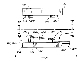
FIGS . 13-27 shows an embodiment of this invention wherein a hollow plastic
radome 301 provides a substantially sealed internal radome cavity that contains a
microstrip antenna having planar or curved radiation and ground plane elements. as
10 above described. While the invention is not to be limited thereto, an embodiment of the
invention used ABS resin, an acrylonitrile-butadieine-styrene copolymer, to forrn
randome 301 and its support fixture 315.
Two-piece radome 301 includes a bottom half300 that supports the antenna's
radiating element 302, the antenna's feed cable and connector 303, and the antenna's
15 ground plane element 304. Edge disposed and mating wall portions of top radome half
305 snap-fit, friction-fit or coupled in a similar manner, to the edge disposed and the
mating walls portions ofthe radome's bottom half300, as is best seen in FIG. 19.
In this embodiment of the invention, and as best seen in FIG. 17, top radome
half 305 includes a plurality of internal tabs or fingers 306 that extend downward to
20 physically engage the top surface 307 of ground plane member 304 shown in FIG. 20,
thus ~ ting in ~ g ground plane member 304 nonrnovable in position.
FIG. 14 is a left side view of antenna/radome 301. FIG. 14 shows a
parting, separation, or mating line 308 that exists between the top plastic
portion/half 305 of radome 301 and the bottom plastic portion/half 300 of
25 radome 301. FIG. 23 is a back side view of antenna/radome 301 that is
taken along viewing line 23-23 of FIG. 13. FIG. 23 shows two, two-piece,
radome mounting lugs 308 and 309, and four radome mounting holes 3 10
that are adapted to receive four self-treading mountin~ screws 365 shown in
FIG. 27. As is apparent from the various figures, each of the two mountin~,
CA 022~124~ 1998-10-07
WO 97/38463 PCT/US97/05716
26
lugs 308,309 is made up of a first lug portion 311 that is molded integrally
with top radome half 305 and a second lug portion 312 that is molded
integrally with bottom radome half 300.
FIGS. 24, 25 and 27 show an elongated, beam-type, plastic mounting
5 fixture 315 that has four relatively small diameter holes 316. Holes 316 are
adapted to mate with the four radome mounting holes 310 of FIG. 23. An
elongated slot 317 within fixture 315 operates to relatively tightly and
slideably receive the radome's two mounting lugs 308,309. When radome
301 iS thus screw-mounted on fixture 315, as seen in FIG. 27, fixture 315
10 facilitates mounting the antenna/radome/cable/connector apparatus in a
great variety of operational positions and places, as a relatively large
diameter hole 318 loosely accommodates feed cable 303, for example see the well
known mounting device 363 of FIG. 27.
FIG. 19 shows a nonlimiting but preferred form of the mechanical
15 means by which top radome half 305 is mounted on, or fit to, bottom
radome half 300. This construction and arrangement provides a mating snap
fit, or friction fit 366,367, that is carried at the top portions 322,323 of themating side walls 320,321 of the top/bottom radome halves 305,300,
exclusive of the two top mating wall portions that form an entry hole 319
20 for the antenna's feed-in/feed-out cable 303.
FIG. 15 is a left side exploded view that is similar to FIG. 14 wherein
the top and bottom radome halves 305,300 are shown vertically separated to
expose a side view of the antenna's copper radiating element 302 and the
manner in which radiating element 302 is three-point supported by way of
25 two vertically extending plastic support posts 325,326 and the centrall~
located and upward extending electrical conductor 327 of the antenna's
feed-in/feed-out cable 303.
While FIG. 15 shows a preferred embodiment of the invention
wherein the plane of radiating element or member 302 is inclined to the
CA 022~124~ 1998-10-07
W097/38463 PCT~S97/05716
27
plane of ground plane element or member 304, it is to be within the spirit
and scope of this embodiment of the invention that the two antenna
components 302,304 can be mutually parallel, as is shown in FIG. 15 by the
dotted line 502 position of radiating element 302. In addition, while
5 inclined radiating element 302 is shown in FIG. 15 as being a planar
member, use of a curved and inclined radiating element, as above described,
is also within the spirit and scope of the invention.
As best shown in FIG. 20, cable 303 is of the well known coaxial
type having an external insulating sheath 328, a metal sheath 329 that acts
10 as one cable conductor, an intermediate insulating sheath (not shown), and a
centrally located wire 327 that serves as a second cable conductor. As
described previously, metal sheath 329 is electrically connected and
physically secured to metal ground plane member 304 by way of solder 330,
or the like. Also as described previously, wire 324 electrically connects to,
15 and physically supports a portion of, metal radiating member 302.
With reference primarily to FIGS. 16 and 17, the two radome halves
300,305 individually form about one half of the radome's internal randome
cavity. More specifically, top radome half 305 of FIG. 17 includes a flat,
planar, rectangular and downward facing internal surface 331 whose
20 boarders or edges are surrounded by an upstanding wall 320, an enlarged
portion of which is seen in FIG. 19. Bottom radome half 300 similarly
provides a flat, planar, rectangular and upward facing internal surface 332, a
portion of which is seen in FIG. 16. The boarders or edges of flat surface
332 are surrounded by an upstanding wall 321, an enlarged portion of which
25 is seen in FIG. 19.
As can be see from FIGS. 16,17, the two radome halves 300.305
include a plurality of mating pinlhole friction couplings. More specifically,
and as seen in FIGS. 15 and 17, top radome half 305 includes four corner-
located and downward extending plastic pins 333. Pins 333 are adapted to
CA 022~124~ 1998-10-07
WO 97/38463 PCT/US97/05716
frictionally mate with four holes 334 that are provided in the four corner-
located and upward extending posts 335 that are provided by bottom
radome half 300, see FIG. 16. As will be appreciated~ pins 333 may be
adhesively as well as frictionally secured within holes 334.
A feature of this invention is the manner in which the antenna s
radiating element 302 is physically supported or mounted within the internal
cavity of radome 301. As best seen in FIGS. 15, 18, 20 and 22, a first edge
portion 340 of radiating element 302 is physically elevated to a first distance
342 above a corresponding and underlying first edge portion 341 of ground
plane element 304, as an opposite and second edge portion 343 of radiating
element 302 is physically elevated to a second distance 344 above a
corresponding and underlying second edge portion 344 of ground plane
element 304. As described above, in accordance with a feature of this
invention distances 342,344 are unequal.
FIG. 22 is a partial exploded side view of FIG. 15 that is partially in
section shows the exploded vertical alignment of a portion of the radome's
bottom half 300, a portion of the antenna's bottom metal ground plane
member 304, one of the two plastic support posts325, a portion of the
antenna's top metal radiating element 302, and one of two plastic self-
treading screws 345. As will be appreciated, screws 345 may be threaded
screws, may be self threading screws, or may be pins that operate on a
friction principle.
Bottom radome half 300 is provided with two mating holes 346 that
are aligned with two holes 347 that are provided within ground plane
element 304. Each of the hole pairs 346,347 receives a pin 348 that is
molded onto the bottom of each of the support posts 325. The inclined top
support surface 349 of each post 325 includes a hole 350 that is adapted to
receive a screw 345.
CA 022~124~ 1998-10-07
W097138463 PCT~S97/OS716
29
In this manner, the two plastic dielectric posts 32S serve the dual
purposes of securing ground plane element 304 coincident with the flat
surface 332 of bottom radome half 300, and supporting the first edge
portion 340 of radiating element 302 physically above the corresponding
5 first portion 341 of ground plane element 304.
As explained above, the opposite or second edge portion 343 of
radiating element 343 iS supported above the second corresponding edge
portion 344 of ground plane element 304 by way of the physical strength of
center conductor 327 of cable 303, conductor 327 being secured to
10 radiating element by solder (not shown).
An additional feature of the invention, as described above, is the
manner in which radiating element 302 is constructed so as to enable
movement 35 I thereof (see FIGS. 18 and 21) relative to its underlying
ground plane element 304. As best seen in FIG. 21, this aspect of the
15 invention is provided by two elongated holes 355 and one elongated slot
356 that respectively slideably receive the two screws 345 and wire 327. In
order to adjust operating parameters of the antenna during assembly of
antenna/radome 301, screws 345 are not tightened and wire 327 is not
soldered to radiating element 302 until after adjustment 351 of radiating
20 element 302 has been completed.
While not critical to the invention, exemplary dimensions of this
embodiment of the invention are shown in FIGS . 13 and 14, wherein
dimension 360 was about 2.30 inch, dimension 361 was about 2.253 inch,
dimension 363 was about 2.50 inch, dimension 361 was about 2.70 inch, and
25 dimension 362 was about 0.60 inch.
CA 0225124C, 1998-10-07
WO 97/38463 PCT/US97/05716
While the exemplary preferred embodiments of tne present invention are
described herein with particularity, those having normal skill in the art will recognize
various changes, modifications, additions and applications other than those specifically
mentioned herein without departing from the spirit of this invention. For example, it is
5 possible to include externally accessible adjustment mechanism for radiating element 302
by incorporating a screw ~tt~çhm~nt through radome 301 provided adequate
communication with center conductor 327 is m~int~ined
What is claimed is:
.... . _