Note: Descriptions are shown in the official language in which they were submitted.
CA 02251372 1998-10-09
WO 97/42731 PCT/US97/07413
2 SYSTEM AND METHOD FOR HIGH-SPEED SKEW-
3 INSENSITIVE MULTI-CHANNEL DATA
TRANSMISSION
s
6 BACKGROUND
7
8 Technical Field
9
The invention relates to a system and method for producing a set of
synchronized
11 binary signals from a multi-channel serial signal, and, more particularly,
for receiving
12 multi-channel serial signals, correcting for skew in the sampling of each
serial signal,
13 and synchronizing binary characters in a channel with their counterparts in
other
14 channels.
is
16 Background and Objects of the Invention
17
18 One problem in sampling a serial data stream is the problem of clock skew.
Clock
19 skew occurs when a recovered clock signal, whose phase is used to determine
the time
at which to sample the serial signal, is out of phase with the serial signal.
This can
21 occur, for example, if the wire or other medium carrying the clock signal
is of a
22 different length or density from the wire or other medium carrying the
serial data
23 signal.
24
2s One way of dealing with a skew condition is to oversample the received
serial signal;
2G that it, so sample the received signal more than one time during the
expected duration
27 of each bit signal. By selecting multiple samples, a skew condition can be
detected
28 and, by using the values captured in the majority of the oversamples, and
ignoring
29 minority spurious values captured as a result of skew. A problem with this
approach,
however, is that it fails for large skews, where a majority of oversamples may
actually
31 be of an adjacent transmitted bit rather than of the intended bit. This is
particularly
1.
CA 02251372 2001-03-14
likely to occur when a small skew has been propagated over a length of time,
resulting in a large
accumulated skew. It is therefore desirable to have a means of detecting
occurrences of skew and
adjusting oversampling to compensate for the observed skew and eliminate the
skew in subsequent
oversamples.
It is further desirable to be have a means of combining multiple serial
signals into a single
composite signal, adjusting for any variations in arrival time of each of the
serial signals.
SUMMARY OF THE INVENTION
In accordance with one aspect of the present invention there is an apparatus
for detecting a phase
condition of an oversampled binary signal, said apparatus comprising:
a phase detection logic circuit for receiving as input a plurality of sets of
binary signals
and producing as output a phase detection signal, said phase detection logic
circuit including:
a plurality of phase-detecting cells, each of said phase-detecting cells
receiving as input
one of said plurality of sets of binary signals, determining a phase condition
for said one of said
plurality of sets of phase-aligned data binary signals, and producing as
output one of a plurality of
sets of phase signals indicative of said phase condition; and
an up-down decision logic circuit receiving as input said plurality of sets of
phase signals,
and producing as output a set of composite phase signals.
In accordance with another aspect of the present invention there is provided a
method for detecting
phase error comprising the steps of:
a) oversampling a data signal to generate a string of binary samples;
b) combining a binary sample from a previous oversampling operation and a
binary
sample from a next oversampling operation with the bit string to create a
composite bit string of
binary samples
c) selecting a subset of the composite bit string in response to a phase
selection
signal;
d) dividing the selected subset of the composite string into groups of binary
samples
having a first, second, and third binary sample;
e) selecting one of the groups of binary samples;
f) responsive to all of the binary samples in the selected group having a same
binary
value, generating a control signal to indicate no skew is detected;
g) responsive to the first bit and the second bit in the selected group having
the same
binary value, and the third bit having a different binary value, generating a
control signal
indicating that a downward skew is detected;
2
CA 02251372 2001-03-14
h) responsive to the second bit and the third bit in the selected group having
the same
binary value, and the first bit having the different binary value, generating
a control signal
indicating that an upward skew is detected;
i) repeating steps (e)-(h) for each group of sampled binary values; and
j) generating a phase error signal in response to the control signals
generated from
each group.
In accordance with yet another aspect of the present invention there is
provided an apparatus for
detecting a phase condition of an oversampled binary signal, said apparatus
comprising:
a phase aligning window for receiving as input a plurality of oversampled
binary signals,
deriving a plurality of sets of phase-aligned binary signals by selecting a
predetermined number of
said oversampled binary signals and providing said sets of phase-aligned
binary signals as output;
and
a phase detection logic circuit for receiving as input from said phase
aligning window a
plurality of sets of binary signals and producing as output a phase detection
signal, said phase
detection logic circuit comprising:
a plurality of phase-detecting cells, each of said phase-detecting cells
receiving as input
one of said plurality of sets of binary signals, determining a phase condition
for said one of said
plurality of sets phase-aligned data binary signals, and producing as output
one of a plurality of
sets of phase signals indicative of said phase condition; and
an up-down decision logic circuit receiving as input said plurality of sets of
phase signals,
and producing as output a set of composite phase signals.
Additional features of the invention will become apparent upon examination of
the description that
follows, particularly with reference to the accompanying drawings.
3
CA 02251372 1998-10-09
WO 97/42731 PCT/US97/07413
1 DESCRIPTION OF THE DRAWINGS
2
3 The aspects of the present invention will be better understood by reference
to the
4 drawings, in which:
6 Figure 1 A depicts a conventional sampling of a serial data stream, without
significant
7 clock skew;
8 Figure IB depicts a conventional sampling of a serial data stream, with a
significant
9 clock skew condition;
Figure 2 depicts an overview of an embodiment of the data recovery system of
the
11 present invention;
12 Figure 3 depicts the relationships among received serial data, a reference
clock and a
13 multiphase clock;
14 Figure 4 depicts an example of the operation of the oversampler the present
invention
for a cycle of each phase of a multiphase clock;
16 Figure 5 depicts the operation of the oversampler for a cycle of a
multiphase clock in
17 which samples are significantly out of synchronization;
18 Figure 6 depicts the interaction of the oversampler and a digital phase-
locked loop;
19 Figures 7A through 7D depict the operation of the phase aligning window of
the
present invention;
21 Figure 8 depicts an example of a circuit to implement the phase aligning
window of the
22 present invention;
23 Figure 9 depicts the operation of a phase detection logic circuit of the
present
24 invention;
Figure 10 depicts the operation of a phase-detecting cell of the present
invention;
26 Figure 11 depicts the operation of the up-down decision logic of the
present invention
27 Figure 12 depicts a state diagram for a digital loop filter of the present
invention;
28 Figure 13 depicts a logic diagram of a circuit implementing a digital loop
filter of the
29 present invention;
Figure 14 depicts a state diagram for a finite state machine of the present
invention;
3 I Figure 15 depicts a logic diagram of a circuit implementing the finite
state machine of
32 the present invention;
4
CA 02251372 1998-10-09
WO 97/42731 PCT/US97/07413
1 Figure 16 depicts the frame synchronization circuit of the present
invention;
2 Figure 17 depicts the frame detect logic of the present invention in further
detail;
3 Figure 18 depicts the detection cell of the present invention in detail;
4 Figure 19 depicts the mapping performed by a mapping block in a detection
cell;
Figure 20 depicts the interchannel synchronizer of the present invention;
6 Figure 21 depicts the delay adjustment block of the present invention in
detail;
7 Figure 22 depicts a timeline for the synchronization block of the present
invention in
8 normal operation; and
9 Figure 23 depicts a timeline for the synchronization block of the present
invention
where one 10-bit signal is arriving early.
11
12 DETAILED DESCRIPTION
13
14 Introduction
16 Figure 1 A depicts a conventional sampling of a serial data stream, without
significant
17 clock skew. Received clock signal 1 indicates a clock signal recovered from
an
18 accompanying serial line. PLL clock signal 3 indicates a clock signal
generated by a
19 phase locked loop in response to received clock signal 1. Data is sampled
according to
the PLL clock signal 3. Conventionally, a sample of serial signal 5 is made
with each
21 falling edge of PLL clock signal 3. Figure I A depicts the PLL clock signal
3 in exact
22 synchronization with received serial signal 5, as shown by correct sampling
points 7.
23
24 Figure 1 B depicts the same conventional sampling of a serial data stream,
with a
significant clock skew condition. As in figure I A, received clock signal 1
indicates a
26 clock signal recovered from an accompanying serial line. PLL clock signal 3
indicates
27 a clock signal generated by a phase locked loop in response to received
clock signal I .
28 Data is sampled according to the PLL clock signal 3. However, in the case
depicted in
- 29 figure 1 B, the PLL clock signal 3 is out of phase from serial signal 5.
As a result,
serial signal 5 is not sampled near the center of the bit, but is instead
sampled at
31 incorrect sample point 9. Incorrect sample point 9 is some distance,
represented by
32 skew distance 11, from the optimal sampling point. As a result serial
signal 5 may be
33 incorrectly measured as having a value different from that of the
transmitted value.
5.
CA 02251372 1998-10-09
WO 97/42731 PCT/US97/07413
1
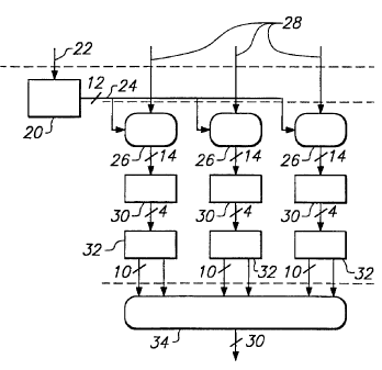
2 Figure 2 depicts an overview of an embodiment of the data recovery system of
the
3 present invention. Charge-pump phase-locked loop (PLL) 20 receives a
transmitted
4 reference clock 22. Concurrent with the transmission of reference clock 22,
one or
more multi-bit block assembly circuits 25 receive as input transmitted serial
data 28,
6 and produce as output a skewless data character. Optionally, each skewless
data
7 character is provided as input to an inter-channel synchronization circuit
34. The inter-
8 channel synchronization circuit 34 selectively delays one or more of the
received
9 skewless characters and produces as output a synchronized multi-channel
signal
comprising each of the received skewless characters. The embodiment depicted
in
11 figure 2 uses multi-bit block assembly circuits to produce a three-channel
composite
12 signal, and is therefore particularly well-suited to the transmission of a
video signal
13 employing a composite RGB signal made up of a signal for each of the Red,
Green and
14 Blue signals used to compose the RGB signal.
16 Each multi-bit block assembly circuit 25 comprises an oversampler 26, a
digital phase-
17 locked loop (DPPL) 30 and a byte synchronizer 32, as is more fully
disclosed herein.
18
19 Oversampler Operation
21 In operation, oversamplers 26 receive as input transmitted serial data 28,
which is
22 transmitted at a predetermined number of bits per second (bps). The
frequency of
23 transmitted reference clock 22 and the bps of transmitted serial data 28 is
chosen so
24 that the number of bits of transmitted serial data 28 transmitted in one
duty cycle of
reference clock 22 is equal to the number of bits in a unit to be decoded,
ordinarily one
26 character. For example, if the invention is implemented to decode a unit of
one ten-bit
27 character at a time, and reference clock 22 has a frequency of N MHz,
serial data 28
28 will be transmitted at the rate of 1 OxN Mbps. For example, if the received
data rate is
29 650 Mbps, reference clock 22 will have a frequency of 65 MHz.
31 In response to reference clock 22, PLL 20 generates a multiphase clock
signal 24.
32 Multiphase clock signal 24 has a frequency and phase such that a plurality
of clock
33 edges are asserted in the amount of time needed for the receipt of each bit
received
6.
CA 02251372 1998-10-09
WO 97/42731 PCT/US97/07413
1 from transmitted serial data 28. For example, a multiphase clock signal 24
having a
2 phase of 12 and having a frequency of 2.SxN MHz enables three clock edges to
be
- 3 asserted for each bit of received serial data 28.
4
Figure 3 depicts the relationships among received serial data 28, reference
clock 22
6 and multiphase clock 24. The depicted embodiment is of a reference clock 22
having a
7 frequency of NMHz, serial data 28 transmitted at l OxN Mbps, and multiphase
clock 24
8 having a phase of 12 and a frequency of 2.SM Hz. Serial data 28 comprises a
plurality
9 of 10 serial data bits 28-1 through 28-10. Multiphase clock 24 comprises a
plurality of
clock signals 24-1 through 24-12, each of which clock signals has a frequency
of 2.SM
11 Hz, and each of which is equally spaced in phase from its adjacent clock
signal. The
12 frequencies of clock signals 24-1 through 24-12 are such that a
predetermined number,
I 3 three in the example, of rising edges of the multiphase clock 24 occur
during each bit
14 28-1 through 28-10. For example, rising edges of clocks 24-I, 24-2 and 24-3
occur
during the duration of bit 28-1; rising edges of clocks 24-4, 24-5 and 24-6
occur
16 during the duration of bit 28-2; and so on.
17
I 8 Figure 4 depicts an example of the operation of oversampler 26 for a cycle
of each of
19 clock 24-1 through 24-12. The example depicted shows four input bits, bits
28-1
through 28-4, being sampled in accordance with clocks 24-1 through 24-12,
producing
21 as output oversampled data 40, designated as 12 binary values S[0:11]. In
the example
22 depicted, bits 28-1 and 28-3 each have a value of'1' and bits 28-2 and 28-4
each have a
23 value of'0'. Bit 28-1 is sampled according to clocks 24-1, 24-2 and 24-3
for a total of
24 three samples, producing oversampled data s[O], S[ I ], and S[2]. Bit 28-2
is sampled
according to clocks 24-4, 24-5 and 24-6 for a total of three samples,
producing
26 oversampled data S[3], S[4], and S[5]. Bit 28-3 is sampled according to
clocks 24-7,
27 24-7 and 24-9 for a total of three samples, producing oversampled data
S[6], S[7], and
28 S[8). Bit 28-4 is sampled according to clocks 24-10, 24-11 and 24-12 for a
total of
29 three samples, producing oversampled data S[9], S[10], and S[11].
31 It will be noted that the example depicted shown in Figure 4 assumes that
clocks 24-1
32 through 24-12 are in perfect synchronization with bits 28-1 through 28-4.
As a result,
33 each of the values of sample sets S[0:2], S[3:5], S[6:8] and S(9: l l J are
correctly
7.
CA 02251372 1998-10-09
WO 97/42731 PCT/US97/07413
1 sampled. In contrast, Figure 5 depicts the operation of the oversampler 26
for a cycle
2 in which clock 24-1 through 24-12 are significantly out of synchronization
with bits
3 28-1 through 28-4. It will be noted that sampled bits S[0] and S[1] sample
the correct
4 received bit 28-1, yielding a correctly sampled value'1', but that sampled
bit S[2]
samples incorrect input bit 28-2 rather than correct received bit 28-1,
resulting in an
6 erroneous value of'0'. Likewise, sampled bits S[3:4], S[6:7] and S[9:10]
correctly
7 sample received bits 28-2, 28-3 and 28-4 respectively. However, sampled bit
S[5]
8 erroneously samples received bit 28-3, sampled bit S[8] erroneously samples
received
9 bit 28-4, and sampled bit S[I1] erroneously samples received bit 28-5.
Despite the
errors in sampling induced by the lack of synchronization, it will be noted
that the
11 center oversampled bit in each group of three (e.g., S[1], S[4], S[7] and
S[10) of
12 groups S[0:2], S[3:5], S[6:8] and S[9:11], respectively) are correctly
sampled despite
13 the skew.
14
Digital Phase Locked Loop Operation Overview
16
17 Figure 6 depicts the interaction of oversampler 26 and DPLL 30, and an
overview of
18 the operation of DPLL 30. Following oversampling, oversampler 26 provides a
14-bit
I 9 signal 60 as output to DPLL 30. the 14-bit signal comprises S[0:11 ] and
two
additional bits. One additional bit is the last bit sampled from the previous
operation of
21 oversampler 26 (i.e., the value sampled for S[I 1] in the previous sampling
iteration),
22 denoted as S'[11]. The other additional bit is the first bit sampled from
the next
23 operation of oversampler 26 (i.e., the value that will be used for S[O] in
the next
24 sampling interation), denoted as S"[0]. in order to obtain the bit value
for S"[0], the
output of oversampler 26 is delayed for one phase of multiphase clock 24.
26
27 DPPL 30 comprises a phase aligning window 50, a phase detection logic
circuit 52, a
28 digital loop filter 54, and a phase-aligning finite state machine (FSM) 56.
Phase
29 aligning window 50 selects 12 of the 14 bits S'[ 11 ], S[0:11 ] and S"[0]
according to the
value of a phase selection signal 58 generated by FSM 56 as more fully
describe herein,
31 thereby producing a 12-bit signal 62. In addition, phase aligning window SO
derives a
' 32 4-bit subset signal from 12-bit signal 62, and provides 4-bit subset
signal 64 as input to
33 byte synchronization circuit 32. Phase selection logic circuit 52 inspects
12-bit signal
8.
CA 02251372 1998-10-09
WO 97/42731 PCT/US97/07413
1 62 and determines whether the signal indicates an out-of phase condition.
Phase
2 selection logic circuit 52 asserts as output two phase detection signals,
UPF 66 and
-- 3 DOWNF 68. Phase detection signals UPF 66 and DOWNF 68 are provided as
input
4 to digital loop filter 54. Digital loop filter 54 determines whether a
sufficient number
S of consecutive phase conditions of like polarity have been detected, and
generates a set
6 of three phase correction recommendation signals denoted as UPT 70, HOLD 72
and
7 DOWNT 74. FSM 56 takes as input signals UPT 70, HOLD 72 and DOWNT 74 and
8 generates a phase selection signal 58, which is used by phase aligning
window 50 as
9 noted above.
1 I The operation and interactions of the various component parts of DPPL 30
will be
12 understood with reference to the detailed description of each component as
set forth
13 herein.
14
I S Phase Aligning Window
16
17 Figures 7A through 7C depict the normal operation of the phase aligning
window S0.
18 As previously described, 14-bit input signal 50 comprises bit S'[ I I ],
twelve bits
19 S[0:11 ] and bit S"[0). Phase aligning window selects 12 bits from 14-bit
input signal
60 to form 12-bit signal 62 denoted as bits Q[0:11 ]. The twelve bits are
selected based
21 on the value of phase selection signal 58. Phase selection signal 58 has
one of three
22 values: '010' indicates that no skew has been detected; ' 100' indicates
that a low skew
23 has been detected; and '001' indicates that a high skew has been detected.
It will be
24 noted that, because phase selection signal 58 has only three values, it may
be
alternatively represented by a two-bit signal. However, the use of one bit for
each
26 skew condition has an advantage of simplifying the digital circuitry needed
to
27 implement the invention.
28
29 Following the production of 12-bit signal Q[0:11 ] 62, the 12-bit signal
will be analyzed
for skew to produce a new value for phase selection signal 58 as disclosed
more fully
31 herein, and the results will be used in fixture iterations of phase
aligning window 50. In
32 addition, phase aligning window 58 selects bits Q[ 1, 4, 7, and 10] and
asserts those for
33 bits as 4-bit signal 64.
9.
CA 02251372 1998-10-09
WO 97/42731 PCT/US97/07413
1
2 Figure 7A depicts the normal operation of phase aligning window 50 when 14-
bit input
3 signal 60 is without skew. Phase selection signal 58 has a value of'O10',
indicating that
4 no sampling skew has been detected, and that therefore no sampling skew
needs to be
corrected. As a result, phase aligning window 50 selects bits S[0:11 ] and
passes the
6 resulting output as 12-bit signal 62. That is, Q[N] is set to the value of
S[N) for each N
7 in the range 0:11.
8
9 Figure 7B depicts the normal operation of phase aligning window 50 when 14-
bit input
signal 60 is expected to be skewed low. Phase selection signal 58 has a value
of 100',
11 indicating that a low skew has been detected, and that therefore a low skew
needs to
12 be corrected. As a result, phase aligning window 50 selects bit S'[ 11 ]
and eleven bits
13 S[0:10] and passes the resulting output as I2-bit signal 62. That is, Q[0]
is set to the
14 value of S'[ 11 ], and Q[N] is set to the value of S[N-1 ] for each N in
the range I :11,
thereby compensating for the detected skew.
16
17 Figure 7C depicts the normal operation of phase aligning window 50 when 14-
bit input
18 signal 60 is expected to be skewed high. Phase selection signal 58 has a
value of'001',
19 indicating that a high skew has been detected, and that therefore a high
skew needs to
be corrected. As a result, phase aligning window 50 selects eleven bits S[
1:11 ] and bit
21 S"[0] and passes the resulting output as 12-bit signal 62. That is, Q[N] is
set to the
22 value of S[N+1 ) for each N in the range 0:10, and Q[ 1 I ] is set to the
value of S"(O],
23 thereby compensating for the detected skew.
24
Figure 7D depicts the operation of phase aligning window 50 when 14-bit input
signal
26 60 is not expected to be skewed, but in fact is skewed low. Phase selection
signal 58
27 has a value of'O10', indicating that no sampling skew has been detected,
and that
28 therefore no sampling skew needs to be corrected. As a result, as in Figure
7A, phase
29 aligning window 50 selects bits S[0:11] and passes the resulting output as
12-bit signal
62. Because phase aligning window 58 did not correct for the skew condition,
the
31 skew condition is retained in 12-bit signal 62 for further analysis as more
fully
32 disclosed herein. It will be noted that despite the skew, 4-bit signal 64
is correctly
33 recovered.
10.
CA 02251372 1998-10-09
WO 97/42731 PCT/US97/07413
1
2 Figure 8 depicts an example of a circuit to implement phase aligning window
50.
- 3 Multiplexor 76 takes as input three 12-bit signals: one 12-bit signal
comprising S'[ 11 ]
4 and S[0:10]; one 12-bit signal comprising S[0:1 I]; and one 12 bit signal
comprising
S S[1:11] and S"[0]. Multiplexor 76 selects among the three 12-bit signals
according to
6 the value of phase selection signal 58 and produces as output 12-bit signal
62 denoted
7 as Q[0:1 I]. 12-bit signal 62 is then passed to phase detection logic
circuit 52 for
8 analysis, and the four bits denoted as Q[1, 4, 7 and 10] are passed to byte
9 synchronizing circuit 32.
I 1 Phase Detection Logic Circuit
12
13 Figure 9 depicts the operation of phase detection logic circuit 52. Phase
detection logic
14 circuit 52 inspects 12-bit signal 62 to determine whether the signal is the
subject of
I 5 skew. phase detection logic circuit 52 comprises a plurality of phase
detecting cells 80
16 and up-down decision logic 82. Bits Q[0:11] are separated into N+1 bit
groups 78
17 comprising three bits each. In a sample embodiment, N is equal to 3 and the
4 bit
18 groups 78 comprise bits Q[0:2], Q[3:5], Q[6:8] and Q[9:11]. Each bit group
78 is
19 provided to a phase-detecting cell 80.
21 Figure 10 depicts the operation of phase-detecting cell 80. The Nth phase
detecting
22 cell 80 takes as input a three-bit group 78 denoted as Q[3N], Q[3N+I ] and
Q[3N+2]
23 where N is a value between 0 and 3 in the sample embodiment. For example,
for N=2,
24 a phase-detecting cell in the sample embodiment will take as input Q[6],
Q[7] and
Q[8].
26
27 If Q[3N], Q[3N+I ] and Q[3N+2] all have the same binary value (i.e., all
three signals
28 are equal to '0' or all three signals are equal to ' 1'), UP[N] and DOWN[N]
are set to '0'
29 to indicate that no skew was detected for this bit group 78. If Q[3N] is
equal in value
to Q[3N+1 ], and different in value from Q[3N+2], UP[N] is set to logic value
'0' and
31 DOWN[N] is set to logic value ' 1', to indicate that a downward skew was
detected for
32 bit group 78. If Q[3N+1 ] is equal in value to Q[3N+2], and difFerent in
value from
11.
CA 02251372 1998-10-09
WO 97/42731 PCT/US97/07413
I Q[3N], UP[N] is set to logic value'1' and DOWN[N] is set to logic value'0',
to
2 indicate that a downward skew was detected for bit group 78.
3
4 Following evaluation of all N+1 bit groups 78 to produce N+I sets of UP[N]
and
DOWN[N] signals, up-down decision logic 82 evaluates the UP[N] and DOWN[N]
6 signals to determine whether sufficient skew was detected to recommend a
phase
7 adjustment. Figure 11 depicts the operation of up-down decision logic 82. Up-
down
8 decision logic 82 provides UP[O:N] as input to adder 84. Adder 84 sums the
number
9 of'1' signals asserted in the UP[O:N] signal set and provides the sum to
comparator 86.
Comparator 86 sets signal UPF 66 to a logic value ' 1' if the count is greater
or equal to
I 1 2, and to logic value '0' otherwise. Likewise, up-down decision logic 82
provides
12 DOWN[O:N] as input to adder 88. Adder 88 sums the number of'1' signals
asserted in
13 the DOWN[O:N] signal set and provides the sum to comparator 90. Comparator
90
14 sets signal DOWNF 68 to a logic value ' 1' if the count is greater or equal
to 2, and to
logic value '0' otherwise.
16
17 Referring again to figure 6, phase detection logic circuit 52 passes signal
UPF 66 and
18 signal DOWNF 68 to digital loop filter 54 for additional processing.
19
Digital Loop Filter
21
22 Digital loop filter 54 receives as input signal UPF 66 and signal DOWNF 68.
When a
23 predetermined number (e.g., four) of consecutive signals UPF 66 are
received having a
24 logic value ' 1', digital loop filter 54 sets signal UPT 70 to logic value
' 1' and sets signals
HOLD 72 and DOWNT 74 to logic value'0'. When a predetermined number (e.g.,
26 four) of consecutive signals DOWNF 68 are received having a logic value'1',
digital
27 loop filter 54 sets signal DOWNT 74 to logic value ' 1' and sets signals
HOLD 72 and
28 UPT 70 to logic value'0'. When neither a predetermined number (e.g., four)
of
29 consecutive signals UPF 66 nor a predetermined number (e.g., four) of
consecutive
signals DOWNF 68 are received having a logic value ' 1', digital loop filter
54 sets
31 signal HOLD 72 to logic value'1' and sets signals UPT 70 and DOWNT 74 to
logic
32 value '0'.
12.
CA 02251372 1998-10-09
WO 97/42731 PCT/US97/07413
2 Figure 12 depicts a state diagram for digital loop filter 54. Digital loop
filter 54
3 operates in a plurality of states. Each operating state may be of a type H,
type U, or
4 type D. An H-type state is characterized by asserting a signal HOLD 72 with
a logic
value ' I', asserting a signal UPT 70 having a logic value '0' and asserting a
signal
6 DOWNT 74 having a logic value '0'. A U-type state is characterized by
asserting a
7 signal HOLD 72 with a logic value'0', asserting a signal UPT 70 having a
logic value
8 '1' and asserting a signal DOWNT 74 having a logic value'0'. A D-type state
is
9 characterized by asserting a signal HOLD 72 with a logic value '0',
asserting a signal
UPT 70 having a logic value '0' and asserting a signal DOWNT 74 having a logic
value
11 ' 1'.
12
13 As shown in Figure 12, digital loop filter 54 transits from state to state
in response to
14 received signals UPF 66 and DOWNF 68. Digital Loop Fitter 54 initially
begins
execution in initial H-type state 102. In response to signal UPF 66 having a
logic value
16 ' I', digital loop filter 54 transits to H-type state 104. Upon transiting
to H-type state
17 104, digital loop filter 54 emits a HOLD signal 72 having a logic value '
1', an UPT
18 signal 70 having a logic value '0' and a DOWNT signal 74 having a logic
value '0'. If
19 digital loop filter 54 in H-type state 102 receives a signal DOWNF 68
having a logic
value ' 1', digital loop filter 54 transits to H-type state 114. Upon
transiting to H-type
21 state 114, digital loop filter 54 emits a HOLD signal 72 having a logic
value ' 1', an
22 UPT signal 70 having a logic value '0' and a DOWNT signal 74 having a logic
value '0'.
23 It will be noted that in H-type states 104, 106 and 108, receipt of any
instance of UPF
24 signal 66 having a logic value '0' causes digital loop filter 54 to revert
to initial H-type
state 102. It will likewise be noted that in H-type states 114, 116 and 118,
receipt of
26 any instance of DOWNF signal 68 having a logic value '0' causes digital
loop filter 54
27 to revert to initial H-type state 102.
28
29 After four consecutive instances of an UPF signal 66 having a logic value '
1', digital
loop filter 54 transits to U-type state 110. Upon transiting to U-type state
110, digital
31 loop filter 54 emits a HOLD signal 72 having a logic value '0', an UPT
signal 70 having
32 a logic value ' 1' and a DOWNT signal 74 having a logic value '0'. In the
next iteration,
13.
CA 02251372 1998-10-09
WO 97142731 PCT/US97107413
1 digital loop filter 54 transits to initial H-type state 102 regardless of
the value of UPF
2 signa166.
3
4 Likewise, after four consecutive instances of an DOWNF signal 68 having a
logic
value ' 1', digital loop filter 54 transits to D-type state 120. Upon
transiting to D-type
6 state 120, digital loop filter 54 emits a HOLD signal 72 having a logic
value '0', an
7 UPT signal 70 having a logic value '0' and a DOWNT signal 74 having a logic
value ' 1'.
8 In the next iteration, digital loop filter 54 transits to initial H-type
state 102 regardless
9 of the value of DOWNF signal 68.
I 1 Figure 13 depicts a logic diagram of a circuit implementing digital loop
filter 54.
12
13 Phase-Adjusting Finite State Machine
14
Phase-adjusting finite state machine (FSM) 56 receives as input signal UPT 70,
signal
16 HOLD 72 and signal DOWNT 74. FSM 56 asserts as output a phase selection
signal
17 58 that communicates to oversampler 26 whether to adjust its sampling as
previously
18 disclosed. Phase selection signal 58 is a tristate signal having a value
indicating
19 whether oversampler 26 should adjust its sampling upward, adjust its
sampling
downward, or maintain its current sampling. Phase selection signal 58 is most
21 conveniently implemented by use of a three-bit signal, in which each bit
corresponds to
22 one of the possible states of the signal. For example, bit 0 of the three
bits may
23 indicate a request for an upward adjustment, bit 1 may be used to indicate
a request to
24 maintain the current sampling, and bit 2 may be used to request a downward
adjustment.
26
27 Figure 14 depicts a state diagram for FSM 56. FSM 56 54 operates in a
plurality of
28 states. A first operating state is phase0 state 150. PhaseO state 150 is
characterized by
29 asserting a phase selection signal 58 requesting a downward adjustment,
e.g., having a
logic value'100'. A second operating state is phasel state 152. Phasel state
152 is
31 characterized by asserting a phase selection signal 58 requesting
maintenance of the
32 current sampling configuration, e.g., having a logic value'O10'. A third
operating state
14.
CA 02251372 1998-10-09
WO 97/42731 PCTIUS97/07413
1 is phase2 state 154. Phase2 state 154 is characterized by asserting a phase
selection
2 signal 58 requesting an upward sampling adjustment, e.g., having a logic
value '001'.
- 3
4 FSM 56 transits from one state to another state depending on the values of
input
signals UPT 70, HOLD 72 and DOWN 74 as shown in figure 14. As shown in figure
6 14, FSM transits from state PhaseO 150 to state Phase 1 152 in response to
UPT signal
7 70 having a logic value'1' or to state Phase2 154 in response to DOWNT
signal 74
8 having a logic value ' 1 ; otherwise (i. e., HOLD signal 72 having a logic
value ' 1'), FSM
9 56 remains in state PhaseO 150. Likewise, FSM 56 transits from state Phasel
152 to
state Phase2 154 in response to UPT signal 70 having a logic value ' 1' or to
state
11 PhaseO 150 in response to DOWNT signal 74 having a logic value ' 1';
otherwise (i. e.,
12 HOLD signal 72 having a logic value ' 1'), FSM 56 remains in state Phase 1
152.
13 Finally, FSM 56 transits from state Phase2 154 to state PhaseO I 50 in
response to UPT
14 signal 70 having a logic value ' 1' or to state Phase 1 152 in response to
DOWNT signal
74 having a logic value ' 1 ; otherwise (i.e., HOLD signal 72 having a logic
value '1'),
16 FSM 56 remains in state Phase2 154.
17
18 Figure 15 depicts a logic diagram of a circuit implementing FSM 56.
19
Digital Phase-Locked Loop Output
21
22 As previously described, and as depicted in figures 7A through 7C, phase
aligning
23 window SO selects a subset of bits from 14-bit input signal 60 in
accordance with phase
24 selection signal 58, and presents the subset as 12-bit output signal Q[0:11
] 62.
Additionally, as previously described a four-bit signal 64 comprising bits
Q[1, 4, 7, and
26 10] is passed as output to frame synchronizing circuit 32.
27
28 Frame Synchronizing Circuit
29
Figure 16 depicts a frame synchronization circuit 32 for use with the present
invention.
3 I Frame synchronization circuit 32 takes as input a stream of multiple
instances of 4-bit
' 32 signal 64 and produces as output a stream of 10-bit encoded characters
176 and a data
33 enable signal 174.
15.
CA 02251372 1998-10-09
WO 97/42731 PCT/I1S97/07413
1
2 As shown in Figure 16, frame synchronizer 32 operates under control of 2. SN
MHz
3 clock 182, N/2 MHz clock 184 and N MHz clock 186. Frame synchronizer 32
4 includes an array of 4-bit D-type flip flops (DFFs) 180-1 through 180-5.
Frame
synchronizer 32 takes as input signal Q[1,4,7,10] 64, which is placed in D-
type flip-
6 flop 180-1. In response to 2.5 NMHz clock signal 182 each DFF 180-1 through
180-4
7 transfers its contents to a respective adjacent DFF. That is, on each
assertion of clock
8 signal 182, the DFF 180-S is loaded from DFF 180-4, DFF 180-4 is loaded from
DFF
9 180-3, DFF 180-3 is loaded from DFF 180-2, DFF 180-2 is loaded from DFF 180-
1,
and DFF 180-1 is loaded from input signal Q[1.4.7.10] 64.
11
12 2.5 NMHz clock 182 has five times the frequency of N/2 MHz clock 184.
13 Accordingly, in synchronization with every fifth cycle of 2.SN MHz clock
182, N/2
14 MHz clock 184 is asserted. With each assertion of clock 184, 20-bit DFF I
88 is
loaded with the values present in 4-bit DFFs 180-1 through 180-5. The output
of each
16 DFF 180-1 through 180-5 is denoted as Q'[1b:19], Q'[12:15], Q[8:11],
Q'[4:7], and
17 Q'[0:3], respectively. 20-bit DFF 188 asserts as output two 10-bit signals
Q"[0:9] 192
18 and Q"[10:19] 194 to 20-to-10 multiplexor 190.
19
N/2 N MHz clock 184 additionally serves to control selection for 20-to-10
multiplexor
21 190, which produces as output 10-bit signal 196 denoted as Q"'[0:9]. As a
result,
22 when N/2 MHz clock 184 is firing, 10-bit signal 196 Q"'[0:9] is equal in
value to 10-bit
23 signal 192 Q"(0:9], and otherwise is equal in value to 10-bit signal 194
Q"[ 10:19].
24
In response to NMHz clock signal 186, 10-bit DFF 200-2 loads a 10-bit signal
from
26 10-bit DFF 200-1 and 10-bit DFF 200-1 loads 10-bit signal Q"'[0:9] 196 from
20-to-10
27 multiplexor 190. In addition, 10-bit DFF 200-I and 10-bit DFF 200-2 each
assert a 10-
28 bit signal that together comprise 20-bit signal Q""[0:19] 202. 20-bit
signal Q""[0:19]
29 202 is provided as input to barrel shifter 204 and frame detect logic 206.
31 Figure 17 depicts frame detect logic 206 in fi~rther detail. Frame detect
logic 206
32 takes as input 20-bit signal Q""[0:19] 202 and produces as output 10-bit
signal
33 BOUND 208 and frame edge detect signal DE 210. Frame detect logic 206
includes an
16.
CA 02251372 1998-10-09
WO 97/42731 PCT/US97/07413
1 array of detection cells 220-0 through 220-9, each of which take as input 20-
bit signal
2 Q""[0:19] and produce as output a single bit MATCH[0) 222-0 through MATCH[9]
3 222-9 of 10-bit signal MATCH[0:9) 223. Each detection cell 220-0 through 220-
9
4 sets its respective MATCH signal 220-0 through 220-9 to logic value ' I' if
the
detection cell detects two consecutive frame edge characters embedded in 20-
bit signal
6 Q""[0:19) 202. A frame edge character is an out-of band character defined as
any of
7 the 10-bit signals ' 11 O 1 O 1 O 1 O 1', ' 11 O 1010100', '001 O 1 O 1 O
10' or '001 O 1 O I O 1 I'. That is,
8 a frame edge character is a 10-bit signal in which bits 0 and 1 have
identical logic
9 values, and in which the logic values of each bit N is not equal to the
logic value of bit
N- I , for N=2 through 8.
11
12 Figure 18 depicts a detection cell 220 in detail. 20-bit signal Q""[0:19]
202 is supplied
13 as input to mapping block 230. Mapping block 230 selects adjacent bits from
20-bit
14 signal 202 and produces them as two 9-bit signals A[0:8] 232 (comprising
signals 232-
1 S 0 through 232-8} and B[0:8) 234 (comprising signals 234-0 through 234-8).
The bits
16 selected by mapping block 230 for detection cell 0 220-0 through mapping
block 230
17 for detection cell 9 220-9 is shown by the chart in Figure 19.
18
19 Detection cell 220 analyzes A[0:8) 232 and B[0:8] to determine whether a
frame
indicator character has been detected. XNOR gate 240 takes as input A[0) 232-0
and
21 A[ i ] 232-1, and produces a logic value ' 1' if the two inputs are
identical. XOR gates
22 242-1 through 242-7 each take as input adjacent bits A[I) 232-I through
A[8] 232-8
23 and each produce a logic value'1' ifthe two input values are not equal.
B[0:8) is
24 likewise analyzed. That is, XNOR gate 244 takes as input B[0] 234-0 and B[
1 ] 234-1,
and produces a logic value'I' if the two inputs are identical. XOR gates 246-1
through
26 246-7 each take as input adjacent bits B[ 1 ] 234-I through B[8] 234-8 and
each
27 produce a logic value ' 1' if the two input values are not equal. The
output of XNOR
28 gate 240, XOR gates 242-1 through 242-7, XNOR gate 244 and XOR gates 246-1
29 through 246-7 are presented as input to AND gate 248. AND gate produces as
output
I-bit MATCH signal 222. Ifall bits are l, MATCH signal 222 has a logic
value'I',
3 I indicating that two frame edge characters have been detected.
32
17.
CA 02251372 1998-10-09
WO 97/42731 PCT/US97/07413
i Referring again to Figure 17, MATCH signals 220-0 through 220-9 are joined
to form
2 10-bit signal MATCH[0:9] 223, which is presented as input to 10-bit
multiplexor 226.
3 MATCH signals 220-0 through 220-9 are also provides as input to OR gate 225.
OR
4 gate 225 produces as output a control signal 227 for 10-bit multiplexor 226.
If any
detecting cell 220-0 through 220-9 has detected a frame start condition, OR
gate 225
6 will produce as output a logic value ' 1', causing multiplexor 226 to select
signal
7 MATCH[0:9J as output. If a frame edge has not been detected, multiplexor 226
8 instead produces as output the same signal as during the previous NMHz clock
signal.
9 This is accomplished by providing multiplexor 226 output to 10-bit DFF 228.
DFF
I 0 228 is loaded under control of N MHz clock I 86. The output of DFF 228 is
presented
11 as input to multiplexor 226 for selection when control signal 227 has logic
value '0'.
12
13 The output of 10-bit DFF 228 is additionally produced as output signal
BOUND[0:9]
14 208. The output of OR gate 225 is inverted and provided to DFF 229, clocked
synchronously with 10-bit DFF 228 under control of N MHz clock 186. The output
of
16 DFF 229 is presented as data enable signal 210.
17
18 Referring again to figure 16, 10-bit signal BOUND[0:9J 208 is provided as a
control
19 signal to barrel shifter 204. Barrel shifter 204 takes as input 20-bit
signal Q""[0:19]
202. Barrel shifter 204 performs a left shift of 20-bit signal Q""[0:19] 202
under
21 control of 10-bit signal BOUND[0:9] 208. Specifically, barrel shifter 204
left-shifts
22 20-bit signal Q""[0:19] 202 and 10-bit signal BOUND[0:9] 208 simultaneously
until
23 the first bit of 10-bit signal BOUND[0:9] 208 has logic value'1'. That is
barrel shifter
24 204 left-shifts 20-bit signal Q""[0:19] 202 the number of bit positions
equal to the
number of leading logic value '0's in 10-bit signal BOUND[0:9] 208.
26
27 Under control of N MHz clock 186, 10-bit DFF 212 loads 10 bits from barrel
shifter
28 204, and produces as output 10-bit signal T[0:9] 176. In the same clock
cycle, also
29 under control of N MHz clock 186, DFF 214 loads 1-bit DE signal 210 from
frame
detect logic 206 and produces as output DE signal 174.
31
32 DE signal 174 may be used to synchronize multiple parallel serial streams
of 10-bit
33 signal T[0:9] 176 by interchannel synchronizer 34, as will be more fully
described.
18.
CA 02251372 1998-10-09
WO 97/42731 PCT/US97/07413
2 Inter-channel synchronization
3
4 Figure 20 depicts the interchannel synchronizer 24 of the present invention.
Interchannel synchronizer 34 takes as input a plurality of 10-bit signals
T[0:9) 176, one
6 such signal per channel, and a plurality of 1-bit DE signals 174, one such
signal per
7 channel. In the depicted three-channel configuration, three 10-bit signals
TO[0:9) 176-
8 0, T 1 [0:9) 176-1 and T2[0:9) 176-2, and three 1-bit DE signals DEO 174-0,
DE 1 174-
9 2 and DE2 174-2 are received as input.
11 Interchannel synchronizer 34 includes a plurality of delay adjustment
blocks 260, one
12 per channel. Figure 21 depicts delay adjustment block 260 in detail. Each
delay
13 adjustment block 260 takes as input one of I 0-bit signals T[0:9) 174 and
all of DE
14 signals 174. Each delay adjustment block 260 produces as output 10-bit
signal F[0:9)
I 5 264 and data enable signal DE F 266. 10-bit signal F[0:9) is selectively
delayed until it
16 is in synchronization with its associated signals as indicated by data
enable signals for
I7 those associated signals.
18
19 Under control of N Mhz clock 186 10-bit DFF 270 loads T[0:9) 176 and I-bit
DFF
272 loads DE 174. Delay adjustment block 260 also takes as input the DE values
21 corresponding to the other channels, shown as signal DEx 186 and DEy 288.
For
22 example, a delay adjustment block 260 for processing channel 0 would take
10-bit
23 signal TO[0:9] 176-0 for T[0:9) 176 and DEO signal 174-0 for DE signal i
74, and
24 would take DE1 signal 176-I for DEx 286 and DE2 signal 176-2 for DEy 288.
26 Delay decision logic block 274 takes as input the previous value of DE 174,
denoted as
27 DE' 276 and current value of DE 174. Delay decision logic block 274
produces as
28 output a tristate control signal 280, depending on the values of DE and
DE'. If DE'
29 has logic value '0', then control signal 280 has the same value of DE 174.
If DE' has
logic value ' I', the control signal 280 has value '2'. Control signal 280 is
used to
31 control three-way multiplexor 282, which outputs a signal to be loaded to
DFF 284.
32 If control signal 280 has logic value '0', DFF 284 is loaded with a logic
'0'. If control
33 signal 280 has a logic value ' 1', DFF 284 is loaded with a value resulting
from applying
19.
CA 02251372 1998-10-09
WO 97/42731 PCT/US97/07413
1 the other DE signals DEx 286 and DEy 288 to NAND gate 287. If control signal
280
2 has a logic value '2', DFF 284's contents are maintained unchanged.
3
4 The value from DFF 284 is used to control 10-way multiplexor 290 and
multiplexor
S 291. When DFF 284 has logic value '0', I 0-way multiplexor 290 selects 10-
bit signal
6 176, which is loaded into 10-bit DFF 292 on the next cycle of clock 186.
Otherwise,
7 when DFF 284 has logic value'1', 10-way multiplexor 290 selects 10-bit
signal
8 T'[0:9], having a value of 10-bit signal 176 delayed by one clock cycle, and
which is
9 loaded into 10-bit DFF 292 on the next cycle of clock 186. Likewise, When
DFF 284
has logic value'0', 10-way multiplexor 291 selects DE signal 174, which is
loaded into.
11 DFF 293 on the next cycle of clock 186. Otherwise, when DFF 284 has logic
value
12 ' I', multiplexor 291 selects DE' signal 276, having a value of DE signal
174 delayed by
13 one clock cycle, and which is loaded into. DFF 293 on the next cycle of
clock 186.
14
The contents of 10-bit DFF are output as 10-bit signal F[0:9] 264 and as data
enable
16 signal DE F 266, indicating the validity of 10-bit signal 264. Referring
again to figure
17 20, the plurality of signals 264-0, 264-1 and 264-2 provide synchronized
parallel
18 encoded characters. DE F signals 266-l, 266-2 and 266-3 are high when the
contents
I 9 of all three 10-bit signals are valid. The three DE F signals 266-1, 266-2
and 266-3
are ANDed together by AND gate 262, which produced composite DF signal 268,
21 having a logic value ' 1' when all I 0-bit signals are valid and in
synchronization.
22
23 After synchronization, synchronized 10-bit signals FO 264-0, F1 264-1 and
F2 264-2
24 may be provided to a lOBl8B binary decoder to translate the 10-bit-encoded
signals to
8-bit characters for use in a computer system using 8 bits per character,
e.g., ASCII,
26 BCD or EBCDIC.
27
28 Figure 22~depicts a timeline for synchronization block 34 in normal
operation, that is,
29 where no 10-bit signal need to be delayed. Each of 10-bit signals 176-0,
176-1 and
176-2 are already in synch, as shown by their respective data enable signals
174-0,
31 174-1 and 174-2. Each signal is uniformly delayed by one clock cycle, as
shown by
32 10-bit signals 264-0, 264-1 and 264-2.
20.
CA 02251372 1998-10-09
WO 97!42731 PCT1US97/07413
1
2 Figure 23 depicts a timeline for synchronization block 34 in where one 10-
bit signal is
3 arriving early. 10-bit signal 176-0 is shown arriving one clock cycle ahead
of 10-bit
4 signals 176-I and 176-2. This is known because at time T0, data enable
signal 174-0 is
high, while data enable signals 174-1 and 174-2 are set low. 10-bit signal DEO
174-0
6 is therefore delayed an additional clock cycle beyond 10-bit signals 176-1
and 176-2,
7 so that all of 10-bit signals FO 264-0, Fl 264-1 and F2 264-2 are produced
in
8 synchronization at time T2.
21.