Note: Descriptions are shown in the official language in which they were submitted.
CA 022~14~ 1998-10-22
TITLE:
Computing System having Fault Cont~inment
FIELD OF THE INVENTION:
The present invention relates to a CO~ uLillg system, and more particularly to a fault
tolerant computing system having multiple processor and multiple memory modules that
limit access between modules, in order to facilitate the cont~inment of hardware faults.
BACKGROUND OF THE INVENTION:
Conventional computing devices typically comprise a single central processing unit,
interconnected with a single memory device. The memory device typically has a large
15 storage capacity having numerous memory cells. Each individual memory cell stores an
item of data, typically a byte or word, and is accessed by a unique memory address.
Software written for such a system executes sequentially. Multiple processes on such a
system may similarly be executed sequentially, with each process executing on the central
processor for a slice of time. Each process is allocated its own working memory. Shared
20 memory may be accessed by individual processes. In order to m~int~in shared memory
integrity, software semaphores are used to limit memory access.
CA 022~14~ 1998-10-22
As will be appreciated, the failure of the central proces~ing unit, or the memory
device in such a conventional device typically results in system failure.
As computing demands have grown, demand for multi-processor systems has been
5 created. A multi-processor system may execute program processes simultaneously across
processors. However, multi-processor systems are very susceptible to faults in memory
that is shared among the processes and processors ("shared memory"). As will be
appreciated, the shared memory will contain the state of the system. As such, co-
ordination of access to shared memory must be carefully controlled in order to avoid one
10 process undesirably and unpredictably modifying memory used by another process.
Additionally, as the shared memory is used by all processes and all processors,
failure of shared memory may cause failure of the entire system. Certain applications, such
as for example telephony switches, require extremely high availability and hence fault
15 tolerance.
On the other hand, a multi-processor, shared system, may be designed to allow for
processor and memory redlm-l~nry allowing for the failure of one or more memory devices
and processors. Once recllln~l~n~y is considered, however, the effects of a failed memory
20 or processor module on shared memory must also be considered. More particularly, it is
desirable to protect the state of shared memory in the presence of a hardware failure, to
minimi7e the impact of such a failure.
CA 022~14~ 1998-10-22
The state of shared memory in the presence of a hardware failure may be protected
in two ways: 1) reversible changes made to the failed hardware, prior to its failure may be
rolled back; and 2) future access to the shared memory by the failed hardware may be
inhibited.
A mechanism assuring that shared memory is only modified upon completion of any
process is disclosed in co-pending U.S. patent application no. 08/774,548, the contents of
which are hereby incorporated herein by reference.
Future access to shared memory by failed hardware could be inhibited using known
fail-stop techniques. For example, the failed hardware could be adapted to cease future
access to shared memory as soon as the hardware detected the failure. This, however, does
not prevent memory access if the failed hardware mistakenly resumes operation after an
initial failure. Moreover, it relies on the predictable behaviour of failed hardware.
Accordingly, a method and system of locking out failed hardware in order to limit
access to rem~ining hardware is desirable.
SUMMARY OF THE INVENTION:
It is an object of the present invention, to provide a highly fault tolerant multi-
processor co~ ulhlg system with shared memory.
CA 022~14~ 1998-10-22
In accordance with an aspect of the present invention there is provided a
multi-processor computing system comprising: a memory module comprising alterable
memory; a plurality of processing elements; the memory module comprising a plurality of
controllable receive ports, each having a first state permitting alteration of the memory
5 through the port and a second state preventing alteration through the port; each of the
processing elements connected to one of the receive ports to transmit data to the memory
module; each receive port adapted to assume its second state in response to sensing a failure
on a processing element connected to the port.
In accordance with another aspect of the present invention there is provided a
method of limi~ing access to a shared memory module in a multi-processor computing
system, the module comprising a plurality of receive ports each interconnected to a
processing element, the method comprising the steps of: a) detecting a fault at a processing
element at a receive port of the memory module; and b) limi~ing access to the memory
15 module by the processor in response to detecting the fault.
In accordance with a further aspect of the present invention there is provided a
multi-processor CO~ ulillg system comprising: a memory module comprising alterable
memory; a plurality of processing elements interconnected to the memory module; the
20 memory module comprising means to limit access to the module by each of the processing
elements.
CA 022~14~ 1998-10-22
In accordance with yet a further aspect of the present invention there is provided a
multi-processor computing system comprising: a plurality of memory module comprising
alterable memory; a plurality of processing elements; each memory module comprising a
plurality of controllable memory module receive ports, each memory module receive port
5 having a first state pel,lliLLillg alteration of the memory through the memory module receive
port and a second state preventing alteration through the memory module receive port; a
memory module ~ niller for broadcasting data from the memory module; each
processing element comprising: a plurality of processing element receive ports each
interconn~cte~l with a memory module tr~n.~mitter of a memory module; a processing
10 element tr~n.~mitter interconnected with a receive port of each of the memory modules.
In accordance with another aspect of the present invention there is provided a
colllpu~ g system comprising: a plurality of memory modules; a processing element
comprising a processor; the processing element comprising a plurality of controllable
15 receive ports, each having a first state permitting access to the processor by through the
port and a second state limiting access to the processor through the port; each of the
memory modules conn~ctec~ to one of the receive ports to transmit data to the processing
element; each receive port adapted to assume its second state in response to sensing a
failure on a memory module connected to the port.
CA 022~14~ 1998-10-22
BRIEF DESCRIPTION OF THE DRAWING:
In figures which illustrate, by way of example, embodiments of the present
invention,
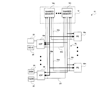
FIG. 1 is a block diagram of a multi-processor, shared memory co~ ,ulh1g system
in accordance with an aspect of the present invention;
FIG. 2 is a block diagram of a shared memory module of the system of FIG. 1;
FIG. 3 is a block diagram of a processing element of the system of FIG. 1;
FIG. 4 is a block diagram of software forming part of the system of FIG 1;
FIG. 5 schematically illustrates a memory read transaction, occurring on the system
of FIG. 1;
FIG. 6 schematically illustrates a memory write transaction, occurring on the system
of FIG. 1; and
FIG. 7 illustrates the format of idle frames used on the system of FIG. 1.
CA 022~14~ 1998-10-22
DETAILED DESCRIPTION:
FIG. 1 illustrates the architecture of a multi-processor, multi-memory co~ ulhlg
system 10 exemplary of a preferred embodiment of the present invention. System 10
5 comprises shared memory 12 which in turn comprises a plurality of shared memory
modules 14a to 14n (collectively and individually 14). Interconnected with shared memory
12 are a plurality of processing elements ("PE"s) 16a to 16m (collectively and individually
16) and a plurality of input/output processors ("IOP"s) 18a to 181 (collectively and
individually 18). Connected to each IOP 18 is one or more input/output peripherals 20.
10 Such peripherals may include disk and tape storage devices or commlmications interfaces
such as OC3 interfaces.
The architecture of system 10 allows scalable processing using one or any other
number of PEs 16, up to the limit of physically available slots. System 10 may be re-
15 configured simply by inserting a further PE 16. Input/output is similarly scalable andaccomplished by inserting more IOPs 18 into system 10. Finally, memory of system 10 is
expandable by increasing shared memory 12 by inserting one or more shared memory
modules 14 up to the limit of physically available slots, or by increasing the memory
capacity of each PE 16 as explained below. In the plefelled embodiment up to ten memory
20 modules 14 may form part of the system, and a m~ximllm of sixteen PEs and IOPs may
form part of the system.
CA 022~14~ 1998-10-22
Additionally, the architecture allows for hardware sparing. More specifically, N +
M sparing may be accomplished. That is, for co~ ulillg capacity that may be met by N
active PEs 16, IOPs 18 or shared memory modules 14, M additionally spare re~-ln-l~nt
modules may be included. In the event one of the modules fails, it may be removed from
5 the system without affecting overall system performance, provided no more than M
modules fail. Scalability and re~llln-l~nry are governed by both the hardware and software
architecture of system 10.
Shared memory 12, PEs 16 and IOPs 18 are interconnected by a set of
10 comm~nication links collectively referred to as an extended architecture interconnect 30
("XAI"). Physically, the XAI 30 comprises links 22a to 221 (individually and collectively
referred to as 22); 24a to 24m (individually and collectively referred to as 24); and 28a to
28n (individually and collectively referred to as 28). These are unidirectional point to
multi-point links. Preferably these are serial links.
Each IOP 18 and PE 16 is interconnected with each shared memory module 14 by
one of links 22 and 24, respectively. These links allow a serial transfer of data from IOPs
18 to shared memory modules 14 and PEs 18 to shared memory modules 14. Each IOP 18
or PE 16 broadcasts all of its outgoing data on one associated link 22 or 24. Each link 22
20 or 24 is interconnected with each shared memory module 14. Thus, all data broadcast by a
single IOP 18 or PE 16 is received by all shared memory cards 14.
CA 022~14~ 1998-10-22
Each shared memory module 14 is further interconn~cte~l with each PE 16 and IOP
18 by a serial link 28. Each of these serial links 28 allows a serial tlan~rel of data from a
shared memory module 14 to all IOPs 18 and PEs 16.
Data is Llall~relled between PEs, IOPs and shared memory modules, 16, 18, and 14respectively, in frames, transferred on links 22, 24 and 28. Groups of frames are used to
complete transactions between modules 16, 18 and 14, as detailed below.
FIG. 2 illustrates the architecture of each shared memory module 14. Specifically,
each memory module 14 comprises a main memory block 32 which, in turn, comprises up
to eight synchronous random access memory ("RAM") hybrids 34 that provide main
program and data storage for the shared memory module 14. The size of memory forsystem 10 is dependent on the capacity of memory block 32 of the shared memory modules
14. This capacity may vary from shared memory module to shared memory module.
At the heart of each shared memory module 14 is a shared memory interface 36.
Further connPcte~l to shared memory interface 36 is ownership memory block 38.
Ownership memory block 38 includes tag memory 40. Tag memory 40 is used by shared
memory module 14 to store information identifying the present state of each group of
thirty-two memory locations within main memory block 32 with respect to the check point
and roll-back strategies as disclosed in U.S. patent application number 08/774,548. As
disclosed in that application, the data within tag memory 40 includes information
, .
CA 022~14~ 1998-10-22
concerning whether a group of memory locations is currently in use by a software task and,
if so, the identifier of that task. The information further identifies whether or not the data
in the group has been modified since the last check point. Tag memory 40 is used and
updated by the check point and data ownership state machines of the shared memory
5 interface 36 as disclosed in that application each time memory block 32 is accessed. This
memory ownership and roll-back scheme allows restoration of shared memory in the event
a process responsible for its modification fails before completion.
Shared memory interface 36 is an application specific integrated circuit ("ASIC")
10 and acts as a memory controller and port controller for memory modules 14.
Forming part of shared memory interface 36 is receive port block 37 and transmit
port 35. Receive port block 37 comprises a plurality of data input ports to shared memory
interface 36, each of which is physically and logically isolated from the other, and serves as
15 the access point for receipt of data from interconnected modules by shared memory
interface 36. Similarly, a data output transmit port 35 forms part of shared memory
interface 36 and allows for the provision of data from shared memory interface 36. Each
port is a lelmillation on a module of a connection to or from another module. Each receive
port is controllable to assume one of at least two states. These states may limit or allow
20 access to a module, thereby effectively isolating another module interconnected with the
port based on the state of the port. The state of the port is controlled by shared memory
interface 36. As noted, each port is a physical port formed on shared memory interface
CA 022~14~ 1998-10-22
36.However, a person skilled in the art will appreciate that the ports need not be physical
ports, but instead could be logical ports. Moreover, the ports need not be formed as part of
the shared memory interface 36.
Interconnected to receive port block 37 and transmit port 35 of shared memory
interface 36 is an XAI interface block 46. Preferably, the XAI interface block 46 is formed
from one or more ASICs. XAI interface block 46 provides the physical link between
shared memory module 14 and the XAI 30.
FIG. 3. illustrates the architecture of each PE 16. PEs 16 provide system 10 with
multiple spared, fault detecting computing engines each operating in a symmetric multi-
processing environment. Each PE 16 m~int~in~ an independent service state duringoperation so that each PE may be individually replaced or upgraded without the need to
replace any other hardware and without causing any other interruption to the system. Each
PE 16 comprises a processor block 50. Each processor block 50 comprises two
microprocessors as central processing units ("CPUs") 52a and 52b. RAM 54 is
interconnected with block 50 and provides fast local access by processors 52a and 52b to a
copy of a program used to control operation of processor block 50, and overall control of
system 10. CPUs 52a and 52b operate in synchronous lock-step with comparisons of their
outputs to enable comprehensive fault detection.
Additionally, interconnected to processor block 50 is a processor system interface
CA 022~14~ 1998-10-22
60. Processor system interface 60 is also formed as an ASIC. Processor system interface
60 provides the interface for PE 16 to the XAI 30 (FIG. 1). Forming part of processor
system interface 60 is a data receive port block 59 and a transmit port 61. Receive port
block 59 provides a plurality of input ports, each of which is physically and logically
5 isolated from the other. These serve as the access points for receipt of data from
interconnected modules by processor system interface 60. Similarly, a data output transmit
port 61 forms part of shared memory interface 36 and allows for the provision of data from
shared memory interface 36.
Interconn~cte~l with receive port block 59 and transmit port 61 of each processor
system interface 60 is an XAI interface block 62. XAI interface block 62 is substantially
identical to XAI interface block 46 of shared memory modules 14 depicted in FIG. 2. XAI
interface block 62 provides the physical interface between each PE 16 and the XAI through
receive port block 59 and transmit port 61.
The architecture of each IOP 18 (FIG. 1) is not illustrated. Ultimately, each IOP
provides a standard PCI interface to system 10 for interconnection to a PCI bus based
peripheral, such as for example a standard serial interface; an optical (OC3) interface; a
SCSI hard disk drive; or a DAT drive. Each IOP also comprises a processor system
20 interface and XAI interface block that are substantially similar to the processor system
interface 60 and XAI interface block 62 forming part of PEs 16.
.
CA 022~14~ 1998-10-22
XAI interface blocks 46 and 62 are illustrated in FIGS. 2 and 3 and comprises a
plurality of pulse receivers ("PRC"s) 80 and at least one pulse tr~n.cmitter ("PTCs") 82 and
82b (see FIG. 2). PTCs 82 and 82b package data received from shared memory interface
36 or processor system interface 60 and broadcast this data on the XAI 30. PRCs 80
receive the transmitted data, and "unpackage" the data to provide it to an interconnected
processor system interface 60 or shared memory interface 36.
Specifically, PRCs 80 of PEs 14 and IOPs 18 receive data from the XAI 30
origin~ting at PTCs 82 or 82b of shared memory modules 14. Similarly PRCs 80 of shared
memory 14 receive data from the XAI 30 origin~ting at PTCs 82 of PEs 14 and IOPs 18.
PTC 82 of IOPs 18 and PEs 16 package data received from interconnected processorsystem interface 60 and broadcast this packaged data on the XAI links 22 or 24 to shared
memory 12. Each PTC 82 broadcasts data to one PRC 80 of each shared memory module
14. Physically, shared memory 12 is located in the centre of system 10. In order to
transmit outgoing data from shared memory module 14 to all PEs 16 and IOPs 18 (FIG. 1),
PTC 82 has mirrored physical outputs at slave PTC 82b. One set of PTC outputs transmits
to all PEs 16 and IOPs 18 to the left of the shared memory module, while the other
transmits to PEs 16 and IOPs 18 located to the right of the shared memory module.
The architecture of the software used in system 10 is illustrated in FIG. 4 and
marked generally 90. Specifically, software system 90 comprises a base layer 96 that
interfaces with the hardware of system 10 and includes an opelaLillg system 102 and
CA 022~14~ 1998-10-22
maintenance software 104. Ultimately, these support product layers and telecom layer 112,
that allow system 10 to act as a telecommunications switch.
Identical copies of the program portion of software system 90 are stored in RAM 54
of each PE 16. Simultaneously running copies of the program portion of the software
system arbitrate overall system co-ordination and schedllling of processing using shared
memory 14.
Access between PEs, IOPs and shared memory modules, 14, 16 and 18 is
accomplished by initi~ting and completing transactions between modules transferred on
XAI 30. Each transaction requires sending frames of data across one or more links 22, 24
and 28. Interspersed between frames of data are "idle codes" comprising repeating bit
sequences, as detailed below. The flow of read and write transactions between PEs 16 and
shared memory modules is illustrated in FIGS. 5 and 6.
As illustrated in FIG. 5, a read transaction is initiated by a PE 16, for example PE
16a. Processor system interface 60 of PE 16a generates a request frame consisting of a
request type; an address; a sequence number; and a source identifier identifying the
origin~ting PE 16a. This frame is llall~r~lled to interconnected PTC 82, packaged and
broadcast to all shared memory modules 14 on link 24a (step S202).
At each of shared memory modules 14, the broadcast frame is received at a single
14
~ . .
CA 022~14~ 1998-10-22
PRC 80 connected to link 22a. The frame is "unpackaged" at the PRC 80 and Sharedmemory interface 36 of memory modules 14 screens the frame and analyzes the
accompanying read address. The shared memory interface 36 uses the read address to
determine whether or not a particular frame is destined for a particular shared memory
module 14. Specifically, shared memory interface 36 of all memory modules 14 receive
the frame and compare the address of the transaction to addresses to which the module is
programmed to respond. If a frame is not intended for a recipient module, it is simply
discarded at the shared memory interface 36 of the recipient module 14. Typically, two or
more shared memory modules 14 operate in redl-n~n~y. As such, more than a singlemodule will be programmed to respond to a particular single address and therefore respond
to the read request.
Shared memory interfaces 36 of memory modules that are programmed to respond
to the address form appropriate response frames. The response frames contain the data
requested; the sequence number from the request; an identifier of the responding memory
module; a destination identifier formed from the source identifier of the request frame; and
a status indicator. The response frame is passed by shared memory interface 36 to PTCs
82 and 82b of the responding shared memory module 14 (step S204). Additionally, each
shared memory interface of a responding memory module 14 buffers the response frame
until an acknowledge frame (FIG. 6) is received from the initi~ting PE (step S206).
All PEs 16 receive a response frame from one responding shared memory module
CA 022~14~ 1998-10-22
14 at one PRC 82. In the event multiple shared memory modules respond, a response
frame is received at multiple PRCs of each PE. The PRCs unpackage the response frame
and pass the data contained in the frame to the processor system interfaces of the PEs.
IOPs similarly receive data in the frame. Processor system interfaces 60 of all PEs 16
5 compare the destination identifier in the response frame to an identifier of the PE. The
processor system interface 60 of all PEs 16 except the processor system interface of the
transaction origin~ting PE discard the received response frames. Ultimately, the processor
system interface 60 of the PE 16 that originated the request returns the data to associated
on-board CPUs 52a and 52b. Once a response frame is received, the PE sends an
10 acknowledge frame back to the shared memory modules. When the responding shared
memory module(s) 14, receive the acknowledge frame, they discard the buffered response
frame.
As illustrated in FIG. 6, a memory write transaction is initi~ted by a PE 16. An
15 origin~ting PE transmits a request frame cont~ining a request type; an address; data; a
sequence number; and a source identifier, identifying the PE. Again this frame is broadcast
to all shared memory modules on one of links 24 (step S302). Only memory modules
programmed to respond to the address specified in the request frame, process the request.
If memory modules are working in redllnl1~n~y, multiple modules will respond to the
20 request. The responding modules write data to the specified memory addresses.
Thereafter, the memory modules broadcast an acknowledge frame cont~ining the sequence
number of the request, and an identifier, identifying the shared memory module. Again,
16
CA 022~14~ 1998-10-22
this acknowledge frame is broadcast to all PEs 16 on one of the links 28 (step S304).
When the origin:~ting PE receives the acknowledge frame, it discards the write request
frame.
While transaction frames are not being sent between PEs, IOPs, and shared memorymodules, PTCs 82 and 82b of XAI interface blocks 46, 62 and 64 generate and broadcast
idle codes on links 22, 24 and 28. The format of possible idle codes is illustrated in FIG.
7. These idle codes are generated directly by the PTCs 82 and 82b of the XAI interface
blocks 46 and 62.
The particular idle code generated and sent by each port of each XAI interface is
governed by the state of an inhibit input on each PTC 82 and 82b. If the inhibit input is
active, the idle code 130 (inhibit-on) is generated and broadcast. If the inhibit input is
inactive, the idle code 132 (inhibit-off) is generated and broadcast.
The inhibit input of each PTC 82 of a PE 16 or IOP 18 is interconnected with theprocessor system interface 60 associated with that PE or IOP by interconnect 122.
Similarly, the PTCs 82 and 82b of each shared memory module 14 are interconnected with
shared memory interface 36 of the shared memory module by interconnect 120.
The processor system interface 60 and shared memory interface 36 each comprise
an ASIC monitoring functional block, that is interconn~cted within the ASIC to other
,
CA 022~14~ 1998-10-22
functional blocks of the ASIC. Other components of PE 16 and shared memory module 14
are similarly interconnected with functional monitoring blocks (not shown). All these
monitoring blocks are interconnected (logically ORed) to lines 120 and 122, and nltim~tely
to the inhibit input of the PTCs 82 and 82b. The monitoring functional block monitors
5 interconnected functional blocks and components to determine any local module functional
fault.
In the event a fault is detected by one of these monitoring blocks, the inhibit input of
the interconn~cte~l PTC is driven active by line 120 or 122. For shared memory modules
14, the inhibit input for both the master and slave PTCs 82 and 82b is made active. In
response, the idle code broadcast between frames on each link 22, 24 or 28 changes from
that illustrated inhibit-off code 132, to the inhibit-on code 130.
Additionally, each processor system interface 60 and shared memory interface 36
15 continuously monitors each of the receive ports of port block 59 and 37. Each port of
receive block 59 is interconnected with a single PRC 80 on an associated XAI block.
Specifically, the format of idle codes received at the ports is monitored by each processor
system interface 60 and shared memory interface 36. In the event a processor system
interface 60 or shared memory interface 36 detects an inhibit-on idle code 130 at any of its
20 receive ports, the respective processor system interface or shared memory interface inhibits
future frames at that corresponding port. To accomplish this, each processor system
interface 60 and shared memory interface 36 m~int~in.~ 1) a port latched status register; and
18
CA 022~14~ 1998-10-22
2) an port instantaneous state register. Each of these registers contains a single bit for each
of the input ports, forming part of block 37 or 59 and connected to a PRC 82. Anytime an
inhibit-on idle code 130 is detected at a port, the bit of the instantaneous state register
associated with the port is made active by the PRC 82. In response, to sensing an active bit
5 in the instantaneous state register, the processor system interface 60 or shared memory
interface 36 drives the associated latched status register bit active. This permanently
inhibits access through the port. That is, future access through that port is inhibited until
the latched status register bit is made inactive. The latched status register bit may only be
made inactive in response to instructions received from maintenance software 104 (FIG. 4).
10 Thus, renewed access to an inhibited port may only be effected by the maintenance
software 104 executing on a PE 16 associated with a port to which access has not been
inhibited.
In operation, system 10 may initially be in a fully functional state. Shared memory
15 12 is configured so that for each shared memory module 14, another shared memory
module provides redlln(l~nt storage. Schl~dl-ling software forming part of OS 102, causing
execution of processes of application software 114 among various PEs 16. The scheclllling
software keeps track of processes to be executed. The PEs 16 read and write to and from
shared memory by initi~ting and completing read and write transactions. As processes are
20 completed changes to shared memory 12 are committed.
In the event one of PEs 16, for example PE 16a fails, processor system interface 60
19
CA 022~14~ 1998-10-22
of PE 16a may detect a fault and asserts line 120 and thereby the inhibit input of PTC 82 of
PE 16a. The processor system interface 60 will assert line 120 in response to any one of a
multitude of errors detected by the processor system interface 60, including for example a
processor data or address parity error.
PTC 82, in turn, transmits inhibit-on idle codes 130 on link 24a, after completing
tr~n.cmic.cion of any in-progress frame. All shared memory modules 14 receive the inhibit-
on idle codes 130 at their PRCs interconn~cted with link 24a. As a consequence, the
shared memory interfaces 36 of all shared memory modules 14 detect the presence of an
idle inhibit-on code 130 at the receive port, interconnected with the PRC 80 associated with
link 24a. In response, the shared memory interfaces 36 imm~ tely set the a latched port
status register bit for that port. This causes shared memory interface 36 to ignore all data
forwarded to the PRC 82 on link 24a. The port is said to be "locked out". Additionally, a
PE failure message is dispatched by the shared memories to the PEs 16 in bits of a status
15 indicator forming part of the a response frame (FIGS. 5 and 6), as described above. This
causes a hardware exception at recipient PEs, that will be serviced by an exception handler
forming part of the OS 102. In response, the OS 102 executing on the rem~ining PEs
initiates a roll-back of shared memory owned by the process that was executing during the
PE failure. Additionally, the executing process is returned to the top of the scheduler
20 queue. The scheduler may then re-assign the process to another PE for execution.
Maintenance software 104 executing on any of the rem~ining PEs 16b-16n may diagnose
the inhibit state of the port by accessing memory and registers of the failed PE 16a through
CA 022~14~ 1998-10-22
ports on shared memory modules 14 without allowing access of the failed PE 16a to other
modules.
The maintenance software 104 is responsible for m~n~ging the overall hardware of
5 system 10. Among other tasks, the software diagnoses hardware faults; it reconfigures the
system; and it optimizes reliability. Urgent faults are typically handled by an exception
handler, triggered by other hardware. The exception handler will perform a preliminary
analysis of the fault and may schedule later updates to be performed by the maintenance
software. At that time, the mailllenallce software may further diagnose and test the failed
10 hardware. As well, the maintenance software periodically initiates diagnostic processes
that may perform thorough hardware diagnoses and reconfigure system 10 to re-optimize
the system 10 in view of a failure.
Similarly, in the event one of the shared memory modules, for example shared
15 memory module 14a fails, the shared memory interface 36 of that shared memory module
14a asserts the inhibit input of PTCs 82 and 82b of the shared memory module 14a. This,
in turn, causes tr~nsmi~sion of inhibit-on idle codes 130 on line 28a after completion of
tr~n~mi~sion of any frame tr~n~mitted during the detection of a failure.
Once broadcast, the inhibit-on idle code 130 is received by all interconn~ctçd PEs
16 and IOPs 18 at the PRCs 80 interconn~cted with link 28a. Tmm~ tely, upon receipt of
an inhibit-on idle code 130, the ports associated with link 28a are disabled at each shared
21
CA 022~14~ 1998-10-22
memory interface 36. Future data frames received at those ports are ignored. Shared
memory modules 14a will continue to broadcast inhibit-on idle codes, until the memory
module fault has been diagnosed and remedied, and the module is reset as maintenance
software 104 may be able to do.
As the memory modules 14 operate in redl1n~1~nry, failure of a shared memory
module 14 and subsequent lock-out of that module at PEs 16 and IOPs 18 may be
accommodated by using data received from the complementary, recllln~nt shared memory
module without disruption of operation of system 10. Again, maintenance software
10 executing on an active PE may diagnose failure of a shared memory module. In the event
the failure can be diagnosed and corrected, access to the shared memory module can be
restored.
It is worth noting that, in theory, the generation of even a single inhibit-on idle code
sequence could cause lock-out of a shared memory module 14, PE 16 or IOP 18.
However, as there is no error detection associated with the idle codes, PRCs 80 actually
must receive three inhibit-on idle codes before asserting an associated bit of the port
instantaneous state register. As multiple idle codes are typically sent between frames, this
does not impact on the ability of system 10 to detect faults. Thus, even a temporary failure
20 of a module is detectecl and may be diagnosed by maintenance software 104. Moreover, a
mistaken self correction by a failed module will not provide renewed access by a locked-out
module. Only after a failure has been diagnosed by maintenance software 104 will a
22
CA 022~14~ 1998-10-22
previously failed module be allowed renewed access to the rem~ining modules of system
10. This makes system 10 highly fault tolerant as failed modules are quickly recognized,
diagnosed and locked-out to prevent further interference with functioning modules.
Additionally, idle codes in combination with transaction frames include clockingsignals on links 22, 24 and 28. In the event a clocking signal is no longer present on a
link, receive ports interconn~cted with the link will assume their inhibit states and "lock
out" future data origin~ting on the link.
While the above embodiment has been described as comprising numerous ASICs, it
will be appreciated that conventional computer hardware devices could be replace one or
more of the custom developed ASICs. Moreover, while a specific point-to-multipoint
interconnect has been described, it will be appreciated that the described system could
easily be modified to include a transaction bus, a token ring or ethernet interconnections.
Of course, almost infinitely many suitable idle codes may be used. Similar, while PEs 16
and memory modules 14 have been described as physically separate, similar modular
entities could be formed on a single physical assembly.
Further, while the use of controllable ports has been described as providing
particular advantages to protecting shared memory, similar advantages may be achieved by
limi~in~ access by a memory module to a processor through the ports. As will further be
appreciated, each port may have multiple states allowing full, none, or partial access to
23
CA 022~14~ 1998-10-22
interconnected memory modules or interconn~ctecl PEs.
It will be understood that the invention is not limited to the illustrations described
herein which are merely illustrative of a preferred embodiment of carrying out the
5 invention, and which are susceptible to modification of form, size, arrangement of parts
and details of operation. The invention, rather, is intended to encompass all such
modification within its spirit and scope, as defined by the claims.
24