Note: Descriptions are shown in the official language in which they were submitted.
CA 022~1799 1998-10-13
P15947-P0
SPECI~ICATIONS
Synchronizing Signal Detecting Device
s
Technical Field of the Invention
The present invention relates to a synchronizing signal detecting device for
detecting synchronizing signals in digital bro~-lc~cting tran~miscion such as digital CATV
(cable television), communication satellite (CS) digital broadcasting and the like.
Background Art
In digital-signal-tr~n~mi~sion including digital CATV, CS digital broadcasting and
the like, synchronizing signals, error-correcting codes, etc. are added to signals at the
tr~n~mi~ion side before the signals are transmitted. The synchronizing signal
5 (hereinafter called "Sync signal"), among others, is essential for restoring the signals on a
receiver side.
Fig. 7 depicts a format depicting a tr~n~mi~sion sequence and placement of signal
data in vestigial side band (VSB) tr~n~mis~ion employed in the Advanced Television
(ATV) in the U.S. A circuit for detecting this Sync signal (a segment Sync signal in this
20 case) in digital signal transmission such as VSB tran~mi~ion is illustrated as a prior art in
Fig. 8. In the me~ntime, an interval between the adjacent Sync signals in Fig. 7corresponds to 832 symbols.
In Fig. 8, the digital signals transmitted in the format of the VSB tr~n.smi~.sion are
fed into an input terminal 100. The Sync signal included in this input digital signal "a"
2s undergoes a pattern check section 2 where the Sync signal is checked whether its pattern
is matched with the reference pattern of the synchronizing signal. In other words, this
pattern check section 2 checks a signal pattern included in the segment Sync signal
(corresponding to 4 symbols) with the predetermined reference pattern (corresponding to
4 symbols), and when they agree with each other, the pattem check section 2 outputs a
30 high level signal "b". This output signal from the pattem check section 2 is fed into an
CA 022~1799 1998-10-13
agreement detection counter 3, disagreement detection counter 4 and Sync counter 6.
The agreement detection counter 3 counts how many signal patterns agree with thereference pattern in the pattern check section 2. In other words, when a timing signal "c"
from the Sync counter 6 is fed into the agreement detection counter 3, which counts up
one by one provided the output signal "b" from the pattern check section 2 is on a high
level. When the count value reaches to "3", the counter 3 does not count up any more
and stays at "3" even if the output signal "b" is at the high level. When the output signal
"c" is fed into the counter 3, which is reset to "0" provided the output signal "b" from the
pattern check section 2 is at a low level.
0 When the disagreement detection counter 4 receives the timing signal "c" from the
Sync counter 6, it counts up one by one provided the output signal "b" from the pattern
check section 2 is at the low level. When the counted value reaches to "3", the counter 4
does not count up any more and stays at "3" even if the output signal "b" is at the low
level. When the output signal "c" is fed into the counter 4, the counter is reset to "0"
15 provided the output signal "b" from the pattern check section 2 is at the high level.
A Sync detection det~rmin~tion section 5 determines a Sync detection based on
the output signals from the counters 3 and 4. Namely, it outputs a high level signal "f"
indicating a Sync detected status just when an output signal "e" from the counter 4 is
changed to "0" while an output signal "d" from the counter 3 stays at "3". On the other
20 hand, it outputs a low level signal "f" indicating a Sync non-detected status just when the
output signal "e" from the counter 4 changes to "3" while the output signal-"d" from the
counter 3 is "0".
A necessary number of input Sync signals can be changed by resetting the count
set values of the counters 3 and 4 as well as the set value of the Sync detection
2s determination section 5.
The Sync counter 6 outputs a signal "c" that controls timings of the count
operations of the counters 3 and 4 by using the output signal "b" from the pattern check
section 2 and the output signal "f" from the Sync detection ~lete~nin~tion section 5.
Namely, the Sync counter 6 starts counting whenever it receives the output signal "b",
30 when the output signal "f" is on a low level indicating the Sync non-detected status, and
CA 022~1799 1998-10-13
the counter 6 outputs the timing signals "c" for a period of 4 symbols every time after a
lapse of the period corresponding to one segment (equal to 832 symbols.)
When the output signal "f" is on a high level indicating the Sync detected status,
the Sync counter 6 starts counting just when the output signal "f" changes to the high level,
and then outputs a high level timing signals "c" for the period of 4 symbols every time
after the lapse of the period corresponding to one segrnent (equal to 832 symbols.)
While, when the output signal "f" is on a low level, the Sync counter 6 does not output the
timing signal !'c" as long as the one segment period is still active, even the output signal
"b" is given before the period of one segment is lapsed.
0 An operation of the Sync signal detection circuit is described hereinafter by
referring to the timing charts in Figs. 9 and 10.
Fig. 9 depicts an initial stage where a digital signal is just fed through the input
terminal 100. A digital signal "a" [equal to an input signal (a) in Fig. 9] fed into the
input tçrmin~l 100 shown in Fig. 8 is firstly sent to the pattern check section 2. The
1S pattern check section 2 detects a place where the pattern of the segment Sync signal
shown in Fig. 7 exists, and outputs the high level signals "b" [equal to (b) in Fig. 9]
indicating a pattern agreement as well as corresponding to 4 symbols to the agreement
detection counter 3, disagreement detection counter 4 and Sync counter 6 when the
pattern of the segment Sync signal agrees with the reference pattern.
The above counters 3 and 4 count responding to the output signals "b" and the
timing signals "c", and then output resulting signals "d" and "e" [equal to (d) and (e) in
Fig. 9] to the Sync detection ~letçrmin~tion section 5.
In the case of Fig. 9, when the counter 3 receives the timing signal "c", the output
signal "b" from the pattern check section 2 is on a high level, the counter 3 thus counts up
25 by one; however, when the count value reaches to "3", the counter does not count up any
more and keeps "3" [refer to (d) in Fig. 9].
On the other hand, when the counter 4 receives the output signal "c" from the Sync
counter 6, the counter 4 is reset to "0" provided the output signal "b" stays at the high
level [refer to (e) in Fig. 9].
The Sync detection determin~tion section S deterrnines a detection of a Sync
CA 022~1799 1998-10-13
signal by using the count values given from the counters 3 and 4. Namely, the section S
shown in Fig. 8 outputs a high level signal "f" [refer to (f) in Fig. 9] indicating the Sync.
detected status just when (at the timing "ta") the output signal "e" from the counter 4
changes to "0" while the output signal "d" is "3".
s As such, when the Sync. detection determination section S outputs a high level
signal "f" that indicates a status of detecting a Sync signal, a data area shown in Fig. 7 is
correctly located. The data included in this data area thus undergo various processes in
data process circuit (not shown in Fig. 8) afterward.
In the case shown in Fig. 9, the Sync counter 6 outputs high level timing signals
o "c" to the counters 3 and 4 for the period of 4 symbols every time after a lapse of the
period corresponding to one segment (equal to 832 symbols) since the time at the point
"ta" [refer to (f) in Fig. 9] when the output signal "f" changes from the low level (Sync.
non-detected status) to the high level (Sync. detected status).
Fig. 10 depicts a case where a digital signal is fed through the input terminal 100
[refer to Fig. 8], and another digital signal takes over the signal, though on the way, due to,
e.g., switching a receiver (time: "tO".) In this case, the Sync detected status is thus
temporarily changed to the Sync non-detected status due to the switch-over. The
determin~tion section S after~vard shows the Sync detected status again.
In other words, before the signal is switched over (before "tO" in Fig. 10), the20 determination section 5 outputs high level signals "f" indicating the "Sync detected status"
[refer to (f) in Fig. 10]. Since the time when the signal "f" has turned to the high level
indicating the Sync detected status, the Sync counter 6 thus continuously outputs the high
level timing signals "c" [refer to (c) in Fig. 10] for the period of 4 symbols every time
after the lapse of one segment period (= 832 symbols) to the counters 3 and 4. Under
2s this condition, the count values of counters 3 and 4 are "3" and "0" respectively [refer to
(d) and (e) in Fig. 10.]
Based on this status, another input signal takes over the present input signal at the
time "tO". The phases of both these input signals seldom coincide with each other, and
rather they do not coincide in general, therefore, the output period of the signal "b" from
30 the pattern check section 2 becomes longer or shorter than the one segment period (= 832
CA 022~1799 1998-10-13
syrnbols) [refer to (b) in Fig. 10.] The output signal "b" from the section 2 is, therefore,
at a low level when the Sync counter 6 outputs the timing signal "c" (= t0). Theagreement detection counter 3 is thus reset [refer to (d) in Fig. 10]. On the other hand,
the disagreement detection counter 4 counts up one by one every time when receiving the
s timing signal "c". When the count value reaches to "3", the counter 4 does not count up
anymore and keeps the value at "3" [refer to (e) in Fig. 10.]
The Sync detection determination section S outputs the low level signal "f"
indicating the Sync. non-detected status just when (time = t2) the output signal "e" from
the counter 4 changes to "3" while the output signal "d" from the counter 3 is "0" [refer to
0 (f) in Fig. 10.]
When the signal "f" changes from the high level to low level (i.e., from the Sync
detected status to Sync. non-detected status), the Sync counter 6 outputs the high level
timing signals "c" sequentially to the counters 3 and 4 for the period of 4 symbols every
time after the lapse of one segment period (= 832 symbols) from each rising point of the
S input signal "b" fed from the pattern check section 2. For instance, the timing signal "c"
at the time = t3 is produced after one segment period (= 832 symbols) of the output signal
"b" produced at the time=t2' tapped off from the pattern check section 2, because the
output signal "f" tapped off from the determination section S is on a low level [refer to (b)
and (c) in Fig. 10].
In the Sync non-detected status, when the counters 3 and 4 receive the timing
signals (c) tapped off from the Sync counter 6, the agreement counter 3 counts up by one
if the output signal "b" is at a high level (time=t3) and the disagreement counter 4 is reset
to "0". After this, the counter 3 counts up one by one at time=t4 and tS [refer to (d) in
Fig. 10.] When the count value of the counter 3 reaches to "3" while the output signal
2s "e" from the counter 4 is "0" (time=tS), the determination section S outputs again the high
level signal "f" indicating the Sync detected status.
As shown in Fig. 10, when a digital signal fed through the input terminal 100 isswitched over, though on the way of tr~n~mi~sion, to another input digital signal by
switching a receiver, the segment Sync signal must be given twice (at the time=tO' and tl')
30 until the Sync detected status is turned temporarily to the Sync non-detected status by this
CA 022~1799 1998-10-13
signal switch. Further, the segment Sync signal must be given in four times (time=t2', t3,
t4 and tS) before the Sync non-detected status is restored to the Sync ~letecte~l status. In
other words, the segment Sync signal must be given in six times between switching the
signal and restoring to the Sync detected status.
This arrangement gives a protective function to Sync signal detecting systems, for
a lack of a Sync signal due to noises or a lack of data causes malfunction, and the same
pattern as a Sync signal comes into a data area by chance also causes malfunction. This
arrangement can thus prevent the malfunction.
0 The above status is described by referring to the timing charts of Figs. 11 and 12.
Fig. 11 depicts a status where disturbance from outside such as noises deforms the pattern
of a Sync signal included in an input signal "a" when the circuit is Sync detected status
(=the agreement detection counter 3 indicates "3" and the disagreement detection counter
4 indicates "O" while the Sync detection determination section 5 outputs a high level
signal "~' indicating the Sync detection status.)
At this time (=t bl), the pattern check section 2 does not output a high
level signal pulse indicating a pattern agreement, and stays outputting a low
level signal. In this case, when the Sync counter 6 outputs the timing signal
"c", the agreement counter 3 is reset to "0", and the disagreement counter 4
20 indicates "1" on the other hand.
However, these disturbances such as noises and the like occur
suddenly and do not last. Therefore, assume all the Sync ~ign~l~ given after
the time = t b2 have the normal patterns, the pattern check section 2 would
output the high level pulse signal "b" indicating the Sync detected status, the
2s agreement counter 3 thus counts up one by one while the disagreement
counter 4 is reset to "0".
Since the Sync detection determination section 5 outputs the low level signal
indicating the Sync non-detected status under the condition that the counter 3 taps of E the
output signal "d" (=O) and the counter 4 taps ofE the output signal "e" (=3), the
30 determination section 5 does not change immediately to the low level indicating the Sync
CA 022F71799 1998- 10- 13
non-detected status when the Sync signal is distorted temporarily, as shown in Fig. 11, due
to the disturbance. Rather, the section 5 still holds the high level indicating the Sync
detected status, thus the malfunction is prevented.
Fig. 12 depicts the following case; As shown in Fig. 10, a signal is
s switched over to another signal, and the counter 3 thus indicates "0" while the
counter 4 indicates "3" (time= t cO). The section 6 is ready to output the low
level signal indicating the Sync non-detected status. Then, a pattern same as
that of the Sync signal abruptly appears in the data area at the time =t cl, .
At this time (=t cl), the pattern check section 2 outputs the high level
o signal "b" indicating the pattern agreement, and the Sync counter 6 outputs
the timing signal "c" at the time = t c2 responding to the signal "b" after the
lapse of one segment period (= 832 symbols). Between t cl and t c2, the
section 2 supplies the signal "b" to the counter 6; however, the counter 6
neglects these signal "b" as described previously.
lS When the Sync counter 6 outputs the timing signal "c" at the time = t c2,
the output signal "b" from the pattern check section 2 is at a low level.
Although the agreement detection counter 3 indicates "0" while the
disagreement detection counter 4 indicates "3", the Sync detection
determination section 5 keeps outputting the low level signal "f" indicating theSync non-detection status.
In other words, when a pattern same as that of the Sync signal appears
abruptly in the data area, the determination section 6 does not indicate Sync
detected status but stays at the low level indicating Sync non-detected status,
thus the malfunction is prevented.
2s The conventional Sync signal detection circuit indeed prevents
malfunctions against the lack of Sync signal due to noises and lack of data, as
well as the same pattern as the Sync pattern appears in the data area by
chance, but this preventive function works unconditionally even when an
input signal is simply switched over as described above. Therefore, as shown
in Fig. 10, the Sync signal must be given as many as 6 times from the signal
~ . . , ~ .
CA 022~1799 1998-10-13
switch-over until the Sync detected status is indicated again, which delays
detecting a Sync .qign~l -
Disclosure of the Invention
s The present invention addresses the above problem and aims to provide
an improved Sync signal detection circuit which maintains the preventive
function of the conventional circuit, and yet quickly detects the Sync signal
when an input signal is switched over to another signal.
The Sync signal detection device of the present invention comprises the
o following elements in order to address the above problem:
(a) pattern check means for checking a pattern of Sync signal with a
reference pattern,
(b) agreement detection count means for counting a value of pattern
agreements and outputting the count value as an output signal,
1S (c) disagreement detection count means for counting a value of
pattern disagreements and outputting the count value as an output signal,
(d) Sync detection determination means for determining whether the
Sync signal is detected or not based on the output ~ign~ from the agreement
detection means and disagreement detection means, and outputting
information about Sync detected status or Sync non-detected status as an
output signal,
(e) Sync count means for counting a value of symbols that
corresponds to cycles of the Sync signal responding to the output ~ign~ from
the Sync detection determination means and pattern check means, and
2s outputting a timing signal when the count value reaches to a predetermined
value, and the Sync signal detection device further comprises:
(f) Sync detection initialization means for receiving a switching
signal that indicates an input signal is switched over, and then forcibly
resetting the agreement detection count means as well as setting the
disagreement detection count means at a predetermined value.
CA 022~1799 1998-10-13
According to the present invention, when a signal is switched over,
the Sync signal can be detected sooner than with the conventional device,
while keeping the following protective function: when a Sync signal is missing
due to noises or a lack of data, or the same pattern as that of a Sync signal
s appears abruptly in the data area by chance, malfunction is prevented.
The invention described in Claim 1 of the present invention refers to a
Sync signal detection circuit comprising:
(a) pattern check means,
(b) agreement detection count means,
o (c) disagreement detection count means,
(d) Sync detection determination means, and
(e) Sync count means.
The Sync signal detection circuit further comprises Sync detection
initialization means that functions as follow: When a signal of input data is
switched over, the initialization means forcibly reset the agreement detection
counter means as well as set the disagreement count means at a
predetermined value responding to a switching signal so that the Sync
detection determination means outputs a signal indicating the Sync non-
detected status. This structure enables the Sync signal detection circuit to
20 detect the Sync signal sooner than the conventional circuit while keeping thepreventive function that prevents the malfunction of detecting Sync ~qignz~l.q.
The invention described in Claim 2 of the present invention refers to a
Sync signal detection circuit comprising:
(a) pattern check means,
2s (b) first agreement detection count means,
(c) disagreement detection count means,
(d) Sync detection determination means, and
(e) first Sync count means for outputting a first timing signal.
The Sync signal detection circuit further comprises the following element:
(f) priority output means comprising:
CA 022~1799 1998-10-13
(f-l) second Sync count means for receiving the output .~ignz~
from the pattern check means, Sync detection determination means and
disagreement detection count means, counting values of symbols that
correspond to a cycle of a Sync signal responsive to these ~ign~l~, and
s outputting second timing ~ign~l~ when the count values reach to
predetermined values,
(f-2) second agreement detection count means for counting a
value of pattern agreement cases where the reference pattern agrees with the
pattern of Sync signal, in response to the output .sign~l~ from the pattern
0 check means and the second Sync count means, and outputting information of
the counted value as an output signal, and
(f-3) OR gate means for gating the output .qi~n~l~ of the first
agreement detection count means and the output signal of the second
agreement detection count means.
S According to this structure, when a signal of input data system is switched
over, the circuit starts checking patterns of Sync ~ign~ responding to the
switching signal. When the checked pattern agrees with the reference
pattern more than one time, the Sync detection signal indicating Sync
detected status is given priority and tapped off from the circuit. This
20 structure enables the circuit to detect Sync .~ign~l~ sooner than the
conventional circuit does when a signal is switched over, while maint~ining
the preventive function, i.e., preventing the malfunction of Sync signal
detection when a Sync signal is missing due to noises or a lack of data~ or
when the same pattern as that of the Sync signal appears in the data area
2s abruptly by chance. Further, this circuit can automatically responds to the
signal switch-over without being given a signal indicating that a signal is to be
switched.
Brief Description of the Drawings
Fig. 1 is a block diagram depicting a Sync signal detection circuit used
, . . . .. . . .
CA 022~1799 1998-10-13
in the first exemplary embodiment of the present invention.
Fig. 2 is a timing chart depicting a detecting operation of the Sync
signal detection circuit shown in Fig. 1.
Fig. 3 is a block diagram depicting a Sync signal detection circuit used
s in the second exemplary embodiment of the present invention.
Fig. 4 is a timing chart depicting a detecting operation of the Sync
signal detection circuit shown in Fig. 2.
Fig. 5 is a timing chart depicting a preventive function against the
malfunction of the Sync signal detection circuit shown in Fig. 3.
o Fig. 6 is a timing chart depicting a preventive function against the
malfunction of the Sync signal detection circuit shown in Fig. 3.
Fig. 7 depicts VSB transmission format utilized in ATV system.
Fig. 8 is a block diagram depicting a conventional Sync signal detection
circuit.
Fig. 9 is a timing chart depicting an operation of the Sync signal
detection circuit shown in Fig. 8.
Fig. 10 is a timing chart depicting a detecting operation of the Sync
signal detection circuit shown in Fig. 8.
Fig. 11 is a timing chart depicting a preventive function against the
20 malfunction of the Sync signal detection circuit shown in Fig. 8.
Fig. 12 is a timing chart depicting a preventive function against the
malfunction of the Sync signal detection circuit shown in Fig. 8.
Exemplary Embodiments of the Present Invention
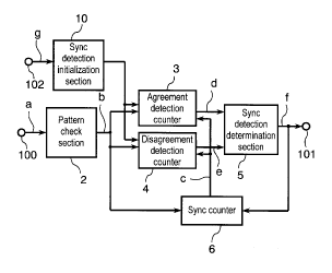
2s Fig. 1 is a block diagram depicting a Sync signal detection circuit used in the first exemplary embodiment of the present invention, and the
corresponding sections to the block diagram depicting a prior art shown in Fig.
8 are designated with the same numbers.
In Fig. 1, a digital signal "a" according to the VSB transmission format
30 is fed into an input terminal 100. A Sync signal included in this digital signal
... ...... .. ... .
CA 022~1799 1998-10-13
"a" is checked in a pattern check section with a reference pattern whether it
agrees with the Sync signal pattern or not. If the reference pattern agrees
with that of the Sync signal, the pattern check section 2 outputs a high level
signal "b", and supplies the signal "b" to an agreement detection counter 3, a
s disagreement detection counter 4 and a Sync counter 6.
A Sync detection determination section 5 determines a Sync detection
based on both of output signals (d and e) that contain the count values of the
counters 3 and 4.
The block diagram depicting the above operation is the same that
o shown in Fig. 8, of which detailed operation and function were already
described, they are thus omitted here.
Exemplary Embodiment 1
The first exemplary embodiment of the present invention (Fig. 1) has an
5 additional structure to the conventional circuit, i.e., a switching signal "g" is
fed into the Sync detection initialization section 10 via an input terminal 102.In other words, when an input signal is switched over to another signal by a
receiver switch (not shown), the signal "g" indicating this signal switching is
fed into the input terminal 102 and then supplied to the Sync detection
20 initialization section 10.
When receiving this switching signal "g", the initialization section 10 is
so structured to forcibly set the agreement detection counter 3 to "0" as well as
the disagreement counter 4 to "3".
The timing chart shown in Fig. 2. describes how to detect Sync .~ign~l~
2s with the Sync signal detection circuit shown in Fig. 1.
In Fig. 2, before a signal is switched over (before the time = t 0), the
Sync detection determination section 5 outputs a high level signal "f"
indicating Sync detected status. The Sync counter 6 thus keeps outputting
high level timing signs~ "c" for a period of 4 symbols to the agreement
30 detection counter 3 and disagreement detection counter 4 every time after one
... .. . . . .
CA 022~1799 1998-10-13
segment period (=832 symbols) passes. And yet, at this stage, the counter 3
indicates "3" and counter 4 indicates "0". [Refer to (d) and (e) in Fig. 2 (d)].In this situation, when another signal takes over the above signal
through a receiver switch or the like (time = t 0), a low level switching signals "g" is fed into the second input terminal 102 responding to this signal switch-
over [refer to (g) in Fig. 2] and supplied to the Sync detection initialization
section 10.
When receiving the switching signal "g" through the second input
terminal 102, the initialization section 10 forcibly sets the counter 3 to "0" as
lO well as the counter 4 to "3" [refer to (d) and (e) in Fig. 2].
These counted values are given to the Sync detection determination
section 5, then the section 6 outputs the low level signal "fi' indicating Sync
non-detected status when the output signal "e" of the counter 4 just changes to
"3" (time = t 0) while the counter 3 outputs the signal "d" at "0" [refer to (f) in
S Fig. 2].
When the output signal "~' from the determination section 5 turns to the
low level indicating Sync non-detected status, the Sync counter 6 outputs high
level timing .sign~ "c" upon receiving an output signal "b" from the pattern
check section 2 to the counters 3 and 4 sequentially for the period of 4 symbols20 every time one segment period (= 832 symbols) passes.
For instance, the timing signal "c" at the time=t2 is produced after one
segment period from the output signal "b" tapped off at the time=tl from the
pattern check section 2 because the output signal "f" indicates Sync non-
detected status (= low level).
2s As such, when the output signal "b" stays at the high level every time atiming signal "c" is given (time= t2, t3, and t4), the agreement detection
counter 3 counts up one by one. When it reaches to "3", the count value "d" is
held at "3" at the time=t5 and onward. When the output signal "b" stays at
the high level every time the timing signal "c" is given (time=t2, t3 and t4), the
30 disagreement detection counter 4 is reset to "0" upon receiving the timing
.
CA 022~1799 1998-10-13
14
signal "c". Then the Sync detection determination section 5 outputs a high
level signal indicating Sync detected status when the counter 3 counts "3" and
the counter 4 counts "0" (time=t4) [refer to (f) in Fig. 2].
Other operations are the same that of the conventional circuit shown in
s Fig. 8, the details are thus omitted here.
In the conventional Sync signal detection circuit shown in Fig. 8, a
segment Sync signal must be given as many as six times from the switch over
of the input signal (time=t 0) until the output from the determination section 5is restored to Sync detected status. However, according to the first exemplary
0 embodiment of the present invention, when the segment Sync signal is given
four times (times = tl, t2, t3 and t4), the output is restored to Sync detectionstatus, as a result, the time for detecting the Sync signal can be shortened.
In the Sync signal detection circuit shown in Fig. 1 used in the first
exemplary embodiment, when the switching signal "g" is not fed through the
second input terminal 102, accordingly, the counters 3 and 4 are not initializedby the Sync detection initialization section 10, the circuit works same as the
conventional circuit in Fig. 8. Therefore, when a Sync signal is missing due
to noises or a lack of data, or the same pattern that of the Sync signal appearsabruptly in the data area, malfunctions can be prevented by the preventive
20 function described above with reference to Figs. 11 and 12.
Exemplary Embodiment 2
The second exemplary embodiment is described by referring to Fig. 3
that is a block diagram depicting the Sync signal detection circuit utilized in
2s this embodiment. The corresponding sections to those in Fig. 8 showing the
prior art are designated with the same numbers.
In Fig. 3, the following elements are the same as those in Fig. 8, the
detailed descriptions thereof are thus omitted here.
This second exemplary embodiment has priority output means in
30 addition to the same elements as the conventional circuit. The priority
. .
CA 022~1799 1998-10-13
output means comprises the following elements: (a) a second agreement
detection counter 23 coupled to the pattern check section 2, (b) a second Sync
counter 26, and (c) an OR gate 11 for the output signal "d" from the agreement
detection counter 3 and the output signal "h" from the second agreement
5 detection counter 23.
When receiving a timing signal "g" tapped off from the second Sync
counter 26, the second agreement detection counter 23 counts up one by one
provided the output signal "b" from the pattern check section 2 is at the high
level. When the count value reaches to "3", the counter 23 does not count up
0 any more and keeps "3" even the output signal "b" is at the high level. When
the output signal "b" is on low level, the counter 23 is reset to "0".
When the disagreement counter 4 taps off the output signal "e" as "0"
and at the same time the Sync detection determination section 5 taps off the
output signal "f" at a high level indicating Sync detected status, the second
5 Sync counter 26 starts counting at the time when signal "~' turns to the high
level. The counter 26 outputs high level timing .si~n~ "g" for a period of 4
symbols every time a period of one segment (=832 symbols) passes. When the
output signal "e" from the counter 4 takes other values [i.e., "1", "2", "3"] than
"0", the second Sync counter 26 starts counting upon receiving each output
20 signal "b" from the pattern check section 2 responding to a rising edge of the
signal "b", and the counter 26 outputs high level timing signal "g" for the
period of 4 symbols every time one segment period (=832 symbols) passes.
Further, when the output signal "e" from the counter 4 takes values other than
"0", the second Sync counter 26 does not output the timing signal "g" even
2s receiving the output signal "b" from the pattern check section 2 before the one
segment period (=832 symbols) passes.
The output signal of OR gate 11 for the output signal "h" of the counter
23 and the output signal "d" of the counter 3 is supplied to the Sync detection
determination section 5. Other elements are the same as those in the prior
30 art shown in Fig. 8, the detailed descriptions thereof are thus omitted here.
CA 022S1799 1998-10-13
16
An operation of the Sync signal detection circuit utilized in the second
exemplary embodiment is described by referring to the timing chart shown in
Fig. 4.
In Fig. 4, before a data signal is switched over (before the time = t 0),
s the Sync detection determination section 5 outputs a high level signal "fi'
indicating Sync detected status. Since when the signal "f~' has turned to high
level (=Sync detected status), the Sync counter 6 thus keeps outputting high
level timing signals "c" for a period of 4 symbols to the agreement detection
counter 3 and disagreement detection counter 4 every time after one segment
o period (=832 symbols) passes. [Refer to (c) in Fig. 4]. Therefore, the counter
3 keeps taking "3" and counter 4 indicates "0" [Refer to (d) and (e) before
time=t 0.]
As previously described, when the counter 4 takes "0" and the Sync
detection determination section 5 outputs high level sign~l.q "f" indicating
S Sync detected status, the second Sync counter 26, upon the signal "f" turningto the high level, keeps outputting high level timing sign~l.q ~g~' to the second
agreement detection counter 23 for a period of 4 symbols every time the one
segment period (=832 symbols) passes. The counter 23 thus holds the count
value at "3". [Refer to (h) before time=t 0 in Fig. 4(h).]
At this stage, when an input signal is switched over to another input
signal by a receiver's switch or the like (not shown) at the time=t 0, an outputperiod of the signal "b" from the pattern check section 2 becomes longer or
shorter than the one segment period (=832 symbols) because both phases of
these two input signals seldom agree with each other, rather they do not agree
2s in general. The output signal "b" from the pattern check section 2 stays thusat low level kefer to (b) in Fig. 4], when the Sync counter 6 taps off the timing
signal "c" (at the time=t 0). Therefore, the agreement counter 3 is reset while
the disagreement counter 4 counts "1". At the times=t 1 and t 2 when both
counters 3 and 4 receive the timing .qign~lq "c" after the time=t 0, the output
30 signal "b" from the pattern check counter 2 is at the low level. The
CA 022~1799 1998-10-13
disagreement counter 4 counts up one by one and holds the count value at "3"
even if the counter would further counts. [Refer to (e) in Fig. 4.]
The Sync detection determination section 5 outputs a low level signal "f'
indicating Sync non-detected status just when the output signal "e" from the
s counter 4 turns to "3" (the time=t 2) while the output signal "d" from the
counter 3 takes "0". [Refer to (f) in Fig. 4.]
On the other hand, the counter 26 starts counting upon receiving each
output signal "b" from the pattern check section 2 responding to a rising edge
of the signal "b," and outputs high level timing ~ign~ 'g," for a period of 4
0 symbols every time a period of one segment (=832 symbols) passes, to the
second agreement detection counter 23, when the output signal "e" from the
counter 4 takes other values [in this embodiment, the count value is "1"] than
"0" (time=t 0.)
For instance, since a count value "e" of the counter 4 is "1" (=other than
S "0") at the time=t 0, the second Sync counter 26 starts counting from a risingedge of the output signal "b" produced at time=t 0', and the timing signal "g" is
produced after one segment period (=832 symbols) passes (time=t 1'.) [Refer
to (g) in Fig. 4.]
When receiving the timing signal "g" from the counter 26 (time=t 0), the
20 second agreement counter 23 resets its count value to "0" provided the output signal "b" from the pattern check counter 2 is at the low level. When
receiving the next timing signal "g" (time=t 1'), the count value "h" of the
counter 23 goes up to "1" provided the output signal is at the high level. Afterthis, the counter 23 counts up one by one (time=t 2', t 3) and when the count
2s value reaches to "3", the counter does not count up any more and keeps "3"
even if the output signal "b" is at the high level (time= t 4, t 5.)[Refer to (h) in
Fig. 4.]
When the count value of counter 23 reaches to "3" (time=t 3,) the
counter value (d) of counter 3 is "1" and that (=e) of the counter 4 is "0".
30 However, the Sync detection determination section 5 outputs the high level
... ., ... ~ , . ..
CA 022~1799 1998-10-13
18
signal "f" indicating Sync detected status because the count value "3" from the
counter 23 is fed via the OR gate 11 as well as the count value "0" from the
counter 4 to the section 5. [Refer to (f) in Fig. 4.]
As such, this second exemplary embodiment proves that Sync signal
s detection circuit of the present invention is restored to Sync detected statuswhen the segment Sync sign~l~ are given four times [times=t 0', t 1', t 2' and t3' as shown (a) in Fig. 4] whereby the time necessary for detecting a Sync
signal is shortened, while the conventional circuit requires 6 times input of the
segment Sync ~ign~ since when an input signal is switched over until an
0 output from the Sync detection determination section 5 indicates the Sync
detected status again as shown in Fig. 8.
The following protective function is still secured in the Sync signal
detection circuit shown in Fig.~3 and utilized in this second exemplary
embodiment: malfunction due to missing of Sync .~ign~ due to noises or a
S lack of data, and malfunction due to an abrupt appearance of the same pattern
as that of a Sync signal in the data area. This is described by referring to thetiming charts shown in Figs. 5 and 6.
Fig. 5 depicts a case where the circuit is in the Sync detected status (i.e.,
a count value of the agreement detection counter 3 indicates "3" and that (=e)
20 of the disagreement detection counter 4 indicates "0", and the Sync detectiondetermination section 5 outputs a high level signal "f"), and a Sync signal
pattern included in an input signal "a" is temporarily distorted (at the time=t
dl) by a disturbance such as noises or the like.
At this time (=t dl), the pattern check section 2 does not output a pulse
2s of four symbols period at the high level that indicates Sync detected status,and the output signal "b" stays at the low level. In this case, when the Sync
counter 6 outputs the timing signal "c", the counter 3 is reset to "0" and the
counter 4 indicates "1". Further, when the second Sync counter 26 outputs
the timing signal "g", the second agreement detection counter 26 is reset to "0"30 because the output signal "b" from the pattern check section 2 stays at the low
CA 022~1799 1998-10-13
.
19
level.
However, the disturbances such as noises and the like happen abruptly
and do not last. Therefore, if the Sync .~ l.s to be received after the next
timing (=t d2) are normal, the pattern check section 2 outputs the high level
s pulse(=four symbols period) .sign~l.s "b" indicating Sync detected status. Thus
after the time=t d2, the counter counts up one by one from "1" while the
counter 4 is reset to "0" [Refer to (d) and (e) in Fig. 6.]
When the output "e" from the counter 4 is "1" at the time=t dl, the
pattern check section 2 does not output "b", therefore, the second Sync counter
o 26 does not tap off the timing signal "g" at the time=t d2. The output signal
"h" from the second agreement detection counter 23 thus stays at "0". After
the time=t d3, the second Sync counter 26 outputs the timing signal "g" every
time one segment period passes, thereby the counter 23 counts up one by one.
Accordingly, the Sync signal detection circuit of the present invention
5 shown in Fig. 3 can prevent a malfunction, i.e., if a Sync signal is temporarily
distorted due to noises or the like, the circuit does not instantly turn to Sync
non-detected status (=low level) but it maintains the high level indicating
Sync detected status, the malfunction is thus prevented.
Fig. 6 depicts a ~imil~qr situation to Fig. 4, i.e., for instance, a signal is
20 switched over at the time=t el, and after the time= t e3 when the Sync
detection determination section 5 is ready to output a low level signal
indicating Sync non-detected status (the output signal "d" from the agreement
detection counter 3 is "0", and the output signal "e" from the disagreement
detection counter 4 is "3"), further at the time =t e3, the same pattern as that
2s of a Sync signal appears by chance in the data area.
At this time (=t e3), the pattern check section 2 outputs a high level
signal "b" indicating a pattern agreement, then the Sync counter 6 outputs the
timing signal "c" responsive to the signal "b" after one segment period (=832
symbols) passes (time=t e5). Meanwhile, the output signal "b" from the
30 pattern check section 2 is fed into the Sync counter 6 between t e3 and t e5
CA 022~1799 1998-10-13
(time=t e4), however, the Sync counter 6 neglects this signal "b" as described
prevlously.
When the timing signal "c" is tapped off from the Sync counter 6 at t e5,
the counter 3 indicates "0" and the counter 4 indicates "3" because the pattern
s check section 2 outputs the low level signal "b".
The second Sync counter 26 outputs the timing signal "g" after one
segment period passes every time the output signal "b" from the pattern check
section 2 is given, except when the output signal "e" from the counter 4 is "0".(e.g., in Fig. 6, the times=t el', t e4, t e6, t e7.. ) Meanwhile, the
o output signal "b" (this is an output signal in the data area and having the
same pattern as that of a Sync signal) is fed into the second Sync counter 26
at the time=t e3 (between t el' and t e4). The second Sync counter 26
neglects this output signal "b" as mentioned previously.
Therefore, when the same pattern as that of a Sync signal appears
S abruptly in the data area, the circuit does not turns to Sync detected status
but keeps outputting the low level signal indicating Sync non-detected status.
The malfunction is thus prevented.
Industrial Applicability
In the digital signal tr~n.~mi~.cion such as a digital television
broadcasting, the present invention proves that a Sync signal can-be detected
in a shorter period than the conventional circuits, further, there is no need togive an indication signal that indicates the signal is to be switched over, to the
circuit of the present invention. Thus the circuit of the present invention can
2s detect a Sync signal automatically within a shorter period, which gives a great
advantage to the practical use of the digital signal tr~n.~mi~sion. The present
invention also preserves the preventive function against the malfunction.
That is when a Sync signal included in transmitted sign~l~ is missing due to
- noises or a lack of data, or the same pattern as that of a Sync signal appears
abruptly in the data area, the circuit mistakenly detects a Sync signal.