Note: Descriptions are shown in the official language in which they were submitted.
CA 02251921 1998-10-14
~.y..-...~ y. ~ p ~ A'fdlt'~1'f~'"'
rt-=.-~. ... ~~s~LATiON
SPECIFICATION
RECEIVER WITH A FREQUENCY OFFSET CORRECTING FUNCTION
TECHNICAL FIELD
The present invention relates to a receiver with a
frequency offset correcting function used for radio digital
data transfer such as that for an automobile telephone.
BACKGROUND ART
Prior to description of the prior art, description is made
for a technological background concerning the present
invention.
Fig. 14 shows a model of a channel with intersymbol
interference (ISI) therein.
The model expresses a channel with a finite impulse
response (FIR) filter. In the model, a received signal is a
synthesized signal synthesized from a lead signal with the
output thereof directly received and a delay signal with the
output thereof received with a delay due to its reflection or
so.
In the figure, a time difference between delay signals
is given by a delay circuit DELAY comprising L-segmented shift
register. The lead signal is obtained by multiplying a
transmitted signal In by channel impulse response (CIR) ca, n as
CA 02251921 1998-10-14
2
a tap coefficient with a multiplier MULTO. Herein, a subscript
n of CIR co,n indicates a time of data received during TDMA
communications .
Also, delay signals are obtained by multiplying delayed
transmitted signals In_1 to In_L by tap coefficients c1, " to cz,
" with multipliers MULT1 to L respectively. Then, outputs of
delay signals from the multipliers MULTO to L are summed up by
a summing device SUM, and an adder (ADD) adds noise Wn to the
summed wave outputted from the summing device ( SUM) to output
the added wave as a received signal rn.
When intersymbol interference ( ISI ) is not present in the
channel, the received signal rn is expressed with the following
equation.
rn = Co n In + Wn . . . ( 1 )
In this case, co, n is a known value, so that a transmitted
signal In can easily be estimated from a received signal rn on
condition that a noise Wn is small.
By the way, according to the model in Fig. 14, when a
transmitted sequence of {In} is transmitted to the channel, this
transmitted sequence undergoes intersymbol interference (ISI)
in addition to additive white Gaussian noise Wn in the channel.
Accordingly, the received signal rn includes not only a time
n but also a transmitting sequence I" in the past before that
time. The received signal at this time is expressed with the
following equation:
CA 02251921 1998-10-14
3
rn = E ci, n In_i + Wn ... (2)
wherein the sum E is obtained for values of i = 0, . . . , L, and
L indicates a time length affected by intersymbol interference
(ISI), namely a channel memory length.
In the model of the channel shown in Fig. 14, the
transmitted sequence In includes a range from time n to time
(n-L). An equalizer is often used for the channel described
above as a device for estimating a transmitted sequence In from
a received signal rn.
Also, when there is frequency offset O m generated due
to a difference between a local oscillator of a transmitter and
a local oscillator of a receiver, a received signal is expressed
with the following equation:
r" = E ci, n In_i exp ( 0 ~n + 8 0) + W'n . . . (3)
wherein 8 o is an initial phase, and W'" is expressed with the
following equation:
w'n = Wn exp (Oc~n + 60) ... (4)
As described above, the performance of a receiver is
deteriorated due to distortion caused by frequency
offset ~ c~ in addition to intersymbol interference ( ISI ) . And
for this reason, the receiver needs to correct the intersymbol
interference (ISI) and also the distortion caused by frequency
offset 0 co .
Next description is made for an example of a receiver with
a frequency offset correcting function based on the
~p,. I JI I Il
CA 02251921 2002-11-25
28964-15
4
conventional technology.
Fig. 15 is a block diagram showing the conventional type
of receiver for correcting frequency offset. The receiver in
this example is the same as that described in "Method and Device
for Compensating Carrier Frequency Offset in TDMA Communication
System (Japanese Patent Laid-open Publication No. HEI 6-
508244)" disclosed by Ling Fuyun et al.
In Fig. 15, designated at the reference numeral 211 is
a CIR estimating circuit for estimating CIR according to a
training sequence in a received signal, at 212 a phase deviation
detecting circuit for computing a phase deviation according to
the CTR estimated value estimated by the CIR estimating circuit
211 and a tail bit described later of the received signal, at
213 an averaging circuit fo~,averaging the phase deviations
outputted from the phase deviation detecting circuit 212 and
computing a frequency offset estimated value, at 214 a frequency
offset correcting circuit for correcting the received signal
rn according to the frequency offset estimated value outputted
from 'the averaging circuit 213, and at 215 an equalizer for
equalizing the received signal r'n corrected by the frequency
offset correcting circuit 214 according to the CIR estimated
value outputted from the CIR estimating circuit 211,
and estimating the transmitted data sequence.
Fig. 16 shows a burst B1 of received signals received
during TDMA communications based on the conventional technology
i ~ i
CA 02251921 2002-11-25
r
28964-15
S
shown in Fig. 15.
In the figure, this burst B1 comprises a training sequence
B11, data sequence B12, B13, and tail bits B14, B15, and the
training sequence B11 and the tail bits B14, B15 are known in
the receiver side.
Next description is made for operations in the example
based on the conventional technology with reference to Fig. 15
and Fig. 16.
At first, the CIR estimating circuit 211 computes, when
having received a received signal r", CIR estimated values go,
g1, . . . , g,, according to the training sequence B11 in the received
burst B1 as shown in Fig. 16 as well as to the training sequence
having previously been known in the receiver side.
Then, the phase deviation detecting circuit 212 first
computes a phase deviation ~m with the following equation
according to the CIR estimated values go,' g1, . . . , gL estimated
with the known training sequence in the received burst B1 by
the CIR estimating circuit 211 as well as to the known tail bits
In-Lfl~ - - -. I"- It should be noted that a subscript m in
the equation indicates a phase deviation in m-th received burst .
CA 02251921 1998-10-14
6
sn ° ~ gi In-i . . . ( 5 )
_ {Im[rn] ' Re [sn] - Im[sn] ' Re [rn] }
/{ABS[rn] ' ABS[Sn] } ... (6)
wherein the sum E is obtained for i = 0, ..., L. It should be
noted that L indicates, as shown in the channel model in Fig.
14, a time length affected by intersymbol interference (ISI),
namely a channel memory length, and corresponds to the number
of stages in the delay circuit DELAY. Also, in the equation,
designated at the reference sign sn is a replica (estimated
value) of a received signal, at Re[a] a real part of a complex
number a, at Im[a] an imaginary part of the complex number a,
and at ABS[a] an absolute value of the complex number a
respectively.
Further, the phase deviation detecting circuit 212
computes a phase deviation per symbol 0 ~ m through the following
equation according to the phase deviation ~ m as described above,
and outputs a result of the computing to the averaging circuit
213.
~m{2/ (M - 1) } . . . (7)
wherein M indicates a total number of symbols of a received burst
B1.
Then, the averaging circuit 213 averages the phase
deviation per symbol ~ ~m estimated for each burst B1, and
outputs a result of averaging to the frequency offset correcting
circuit 214 as a frequency-offset estimated value 0c~m
~ r ~! ! fl
CA 02251921 2002-11-25
..,
2$964-15
The frequency offset correcting circuit 214
corrects frequency offset of a received signal rn through the
following equation according to the frequency-offset
estimated value ~c.~m.
r~~ = r" exp (-j ~ cv~,n) . . . (8)
The equalizer 215 estimates transmitted data sequence
according to the received signal r'" having been subjected to
S offset correction outputted from the frequency offset
correcting circuit 214 as well as to the CIR estimated value
outputted from the CIR estimating circuit 211, and outputs a
result of the decision as a decision value.
However, in the receiver with the conventional type of
frequency offset correcting function, known data such as tail
bits other than the training sequence is required to compute
a frequency-offset estimated value, and also a length of tail
bits in a received signal is generally required to be longer
than a memory length L of the channel, so that transmission
efficiency is worse in turn by the length required for the tail
bits..
In the example based on the conventional technology, a
phase deviation is computed according to the CIR estimated value,
the tail bits and the received signal, so that the phase
deviation to be detected largely varies with noises.
Accordingly, in order to estimate frequency offset with
Q
sufficient precision, it is required to
CA 02251921 1998-10-14
8
suppress variation by making a time constant larger for
averaging phase deviations, and for this reason, when frequency
offset varies with time, it is difficult to follow the variation
in the method described above.
Further, as diversity reception is not performed in the
example based on the conventional technology, an error rate in
decision is higher as compared to the case where diversity
reception is performed.
The present invention has been made for solving the
problems as described above, and it is an object of the present
invention to provide a receiver with a frequency offset
correcting function which has improved the capabilities of
being excellent in transmission efficiency without requiring
known data other than a training sequence, precisely estimating
time-varying frequency offset, and further enabling
performance of diversity reception and determination of data
at a low error rate.
DISCLOSURE OF INVENTION
To achieve the object as described above, the present
invention comprises a frequency offset correcting means for
receiving a received signal as well as a frequency-offset
estimated value and correcting phase rotation due to frequency
offset of the received signal according to the frequency-offset
estimated value; a first channel impulse response estimating
CA 02251921 1998-10-14
- 9
means for estimating channel impulse response at a first
position of the corrected received signal according to a known
training sequence included in the received signal corrected by
the frequency offset correcting means; a determining means for
determining the received signal corrected by the frequency
offset correcting means according to the channel impulse
response estimated value at the first position thereof
estimated by the first channel impulse response estimating
means; a second channel impulse response estimating means for
estimating channel impulse response at a second position apart
from the first position of the corrected received signal
according to the received signal corrected by the frequency
offsetcorrecting means, thechannel impulseresponseestimated
value at the first position thereof estimated by the first
channel impulse response estimating means, and to the value
determined by the determining means; and a frequency-offset
estimated value computing means for computing a frequency-
offset estimated value of the received signal according to the
channel impulse response estimated value at the first position
thereof estimated by the first channel impulse response
estimating means as well as to the channel impulse response
estimated value at the second position thereof estimated by the
second channel impulse response estimating means, and
outputting the computed value to the frequency offset
correcting circuit. Therefore, with this invention, different
CA 02251921 1998-10-14
channel-impulse estimated values at the first and second
positions are obtained according to the training sequence
having been known in the received signal, and a frequency-offset
estimated value is computed according to those phase deviations,
5 so that frequency offset of a received signal can be corrected
and also data can be determined without using known data such
as tail bits other than the training sequence. As a result,
tail bits are not needed as a burst structure of a received signal,
so that transmission efficiency is improved, and also a phase
10 deviation can be computed not according to an estimated value
(replica) of the received signal computed only with tail bits
in a transmission sequence but according to channel impulse
response estimated by sufficiently suppressing a noise element
with an appropriate algorithm (e.g., LMS algorithm), and for
this reason a phase deviation to be detected does not largely
varies with noises, time-varying frequency offset can be
compensated with high precision, and data can be determined at
a low error rate.
The another present invention comprises a frequency
offset correcting means for receiving a received signal as well
as a frequency-offset estimated value and correcting phase
rotation due to frequency offset of the received signal
according to the frequency-offset estimated value; a first
channel impulse response estimating means for estimating
channel impulse response at a first position of the corrected
CA 02251921 1998-10-14
11
received signal according to a known training sequence included
in the received signal corrected by the frequency offset
correcting means; a determining means for determining the
received signal corrected by the frequency offset correcting
means; a second channel impulse response estimating means for
estimating channel impulse response at a second position apart
from the first position of the corrected received signal by
updating the channel impulse response estimated value at the
first position according to the received signal corrected by
the frequency offset correcting means, the channel impulse
response estimated value at the first position thereof
estimated by the first channel impulse response estimating
means, and to the value determined by the determining means;
and a frequency-offset estimated value computing means for
computing a frequency-offset estimated value of the received
signal according to the channel impulse response estimated
value at the first position thereof estimated by the first
channel impulse response estimating means as well as to the
channel impulse response estimated value at the second position
thereof estimated by the second channel impulse response
estimating means, and outputting the computed value to the
frequency offset correcting circuit; and the determining means
determines the received signal corrected by the frequency
offset correcting means, at first, according to the channel
impulse response estimated value at the first position thereof
i ,~ ~. ~~
. . , ~ 02251921 2002-11- .25 . , . . .,~rx=:~-s,~,;
r a
28964-15
12
estimated by the first channel response estimating means, and
determines the received signal corrected by the frequency
offset correcting means, after the second time and
on, according to a value updated from the channel impulse
response estimated value at the first position thereof by the
second channel impulse response estimating means. For this
reason, with this invention, determination of the received
signal after the second time and on is made according to values
obtained, bysuccessively updating the channel impulse response
estimated value at the first position, outputted from the second
estimating means, so that, even when the channel impulse
response estimated value varies with time, the variation can
be followed, and data can be determined at a low error rate .
The another present invention comprises a first channel
impulse response estimating means for estimating channel
impulse response at a first position of the received signal
according to a known training sequence included in the received
signal; a determining means for determining the received signal
according to the channel impulse response estimated value at
the first position thereof estimated by the first channel
impulse response estimating means: a second channel impulse
response estimating means for estimating channel impulse
response at a second position apart from the first position of
the received signal according to the received signal, the
channel impulse response estimated value at the first position
thereof estimated by the first channel impulse response
estimating means, and to the value determined by the determining
means: a frequency-offset estimated value computing means for
i
CA 02251921 2002-11-25
r
28964-15
13
computing a frequency-offset estimated value of the received
signal according to the channel impulse response estimated
value at the first position thereof estimated by the first
channel impulse response estimating means as well as to the
channel impulse response estimated value at the second position
thereof estimated by the second channel impulse response
estimating means; and a local oscillator correcting means for
correcting a frequency from a local oscillator according to the
frequency-offset estimated value computed by the frequency-
offset estimated value computing means. Therefore, with this
invention, a frequency from the local oscillator of the receiver
is directly controlled in place of correcting frequency offset
of the received signal, so that configuration of the circuit
can be simplified.
The another present invention comprises a frequency
offset correcting means for receiving a plurality of received
signals as well as frequency-offset estimated value, and
correcting each phase rotation due to frequency offset for the
plurality of received signalsaccording tothefrequency-offset
estimated value respectively; a first channel impulse response
estimating means for estimating each channel impulse response
CA 02251921 1998-10-14
14
at a first position of the plurality of corrected received
signals according to each known training sequence included in
the plurality of received signals corrected by the frequency
offset correcting means; a determining means for determining
the plurality of received signals corrected by the frequency
offset correcting means according to the channel impulse
response estimated values each at the first position thereof
estimated by the first channel impulse response estimating
means; a second channel impulse response estimating means for
estimating each channel impulse response at a second position
apart from the first position of the plurality of corrected
received signals according to the plurality of received signals
corrected by the frequency offset correcting means, each
channel impulse response estimated value at the first position
of the plurality of corrected received signals estimated by the
first channel impulse response estimating means, and to the
value of the plurality of received signals determined by the
determining means; and a frequency-offset estimated value
computing means forcomputingfrequency-offset estimated value
of the plurality of received signals according to each channel
impulse response estimated value at the first position thereof
estimated by the first channel impulse response estimating
means as well as to each channel impulse response estimated
value at the second position thereof estimated by the second
channel impulse response estimating means, and outputting the
CA 02251921 1998-10-14
computed value to the frequency offset correcting circuit.
Therefore, with this invention, a plurality of received signals
can be received with a plurality of frequency offset correcting
circuits or the like respectively, so that diversity reception
5 can be performed, and data can be determined at a low error rate .
In the present inventions, the frequency-offset
estimated value computing means comprises a phase deviation
detecting means for detecting a phase deviation between the
first position and the second position according to the channel
10 impulse response estimated value at the first position
estimated by the first channel impulse response estimating
means as well as to the channel impulse response estimated value
at the second position estimated by the second channel impulse
response estimating means; and an averaging means for averaging
15 phase deviations obtained by computing a phase deviation per
symbol according to the phase deviation between the first
position and the second position detected by the phase deviation
detecting means to compute a frequency-offset estimated value,
and outputting the computed value to the frequency offset
correcting circuit.
Also, the phase deviation detecting means selects a value
of which the absolute value is the maximum among the channel
impulse response estimated values at the first position
estimated by the first channel impulse response estimating
means, and also selects a value corresponding to the channel
CA 02251921 1998-10-14
16
impulse response estimated value at the first position of which
the absolute value is the maximum among the channel impulse
response estimated values at the second position estimated by
the second channel impulse response estimating means; and
detects a phase deviation of the received signal according to
the product of complex conjugate of the channel impulse response
estimated value at the first position of which the absolute
value is the maximum and the channel impulse response estimated
value at the second position corresponding to the channel
impulse response estimated value at the first position of which
the absolute value is the maximum.
Also, the phase deviation detecting means computes each
product of the complex conjugate of the channel impulse response
estimated value at the first position estimated by the first
channel impulse response estimating means and the channel
impulse response estimated value at the second position
estimated by the second channel impulse response estimating
means, and detects a phase deviation of the received signal
according to the sum of the products each of which the absolute
value is more than a threshold value among the computed
products.
Also, the phase deviation detecting means computes each
product of the complex conjugate of the channel impulse response
estimated value at the first position estimated by the first
channel impulse response estimating means and the channel
CA 02251921 1998-10-14
17
impulse response estimated value at the second position
estimated by the second channel impulse response estimating
means, selects each product of which the absolute value is more
than a threshold value among the computed products, multiplies
each of the absolute values to the selected products, and
detects the phase deviation of the received signals according
to the sum of the multiplied values.
Also, the phase deviation detecting means further
quantizes the phase deviation of the detected received signal,
and outputs a result of the quantization as a phase deviation.
Also, the determining means comprises a soft-decision
equalizer for executing soft-decision of a data sequence in the
corrected received signal according to the received signal
corrected by the frequency offset correcting means as well as
to the channel impulse response estimated value at the first
position estimated by the first channel impulse response
estimating means; and a hard-decision circuit for executing
hard decision of the soft-decision value estimated by the
soft-decision equalizer and outputting a result of the decision
as a decision value of a data sequence in the received signal.
Therefore, with this invention, decision can be made including
reliability by the soft-decision equalizer, so that the
reliability can be utilized in forward error correction and so
on.
I ~L : d. I Ii
CA 02251921 2002-11-25
28964-15
7.8
BRIEF DESCRIPTION OF DRAWINGS
Fig. 1 is a block diagram showing configuration of a
receiver with a frequency offset correcting function according
to Embodiment 1 of the present invention; Fig. 2 is a view
showing a burst structure of the received signal in Embodiment
1; Fig. 3 is a view showing configuration of a determining
circuit - 13a having an equalizer for executing soft-
determination in place of equalizer 13; Fig. 4 is a view showing
another method of computing a CIR estimated value at the second
position; Fig. 5 is a view showing another method of computing
a CIR estimated value; Fig. 6 is a view showing another method
of computing a CIR estimated value: Fig. 7 is a view showing
another~method of computing a CIR estimated value; Fig. 8 is
a view showing another method of computing a CIR estimated
value; Fig. 9 is a view showing another method of computing
a CIR estimated value: Fig. 10 is a view showing a graph of a
quantizing function; Fig. 11 is a block diagram showing
configuration of a receiver with a frequency offset correcting
function according to Embodiment 2 of the present invention;
Fig. 12 is a block diagram showing configuration of a receiver
with a frequency offset correcting function according to
Embodiment 3 of the present invention; Fig. 13 is a block diagram
showing configuration of a receiver with a frequency offset
correcting
l , i~ l i1
CA 02251921 2002-11-25
v
28964-15
19
function according to Embodiment 4 of the present invention;
Fig. 14 is a block diagram showing a model of a channel with
intersymbol interference (IST) therein; Fig. 15 is a block
diagram showing configuration of the receiver with a frequency
offset Correcting function based on the conventional
technology; and Fig. 16 is a view showing a burst structure of
a received signal in the example based on the conventional
technology.
BEST MODE FOR CARRYING OUT THE INVENTION
(1) Embodiment 1
At first, description is made for a receiver with a
frequency offset correcting function according to Embodiment
1 of the'present invention.
Fig. 1 is a block diagram showing configuration of the
receiver with the frequency offset correcting function
according to Embodiment 1 of the present invention.
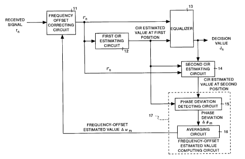
In the figure, designated at the reference numeral I1 is
a frequency offset correcting circuit for correcting a received
signal r" with a frequency-offset estimated value d rim outputted
from an averaging circuit 16 described later; at 12 a first CTR
estimating circuit for estimating CIR at a first position on
a burst according to a training sequence in a recei ved signal
r'~ corrected by the frequency offset correcting circuit 11;
at 13 an equalizer as a determining means for equalizing
~, f ~iJ 11
CA 02251921 2002-11-25
r
28964-15
the received signal r'n corrected by the frequency offset
correcting circuit 11 according to the CIR estimated value at
the first position estimated by the first CIR estimating
circuit 12, and outputting the decision value Jn; at 14 a
second CIR estimating circuit for estimating a CIR estimated
value at a second position apart from the first position on
the burst in a
corrected received signal r'" according to the received signal
r'" corrected by the frequency offset correcting circuit 11,
the CIR estimated value at the first position estimated by the
first CIR estimating circuit 12, and to a result of decision
5 by the equalizer 13; at 15 a phase deviation detecting circuit
for computing a phase deviation according to the CIR estimated
value at the first position estimated by the first CIR
estimating circuit 12 as well°~as to the CIR estimated value at
the second position estimated by the second CIR estimating
10 circuit 14; and at 16 an averaging circuit for averaging the
phase deviations detected by the phase deviation detecting
circuit 15 and computing a frequency offset estimated value.
It should be noted that the phase deviation detecting circuit
15 and averaging circuit 16 constitute a frequency-offset
15 estimated value computing circuit 17.
Fig. 2 shows a burst B2 of the received signal r" in
CA 02251921 1998-10-14
21
Embodiment 1.
In the figure, the burst B2 of the received signal rn in
Embodiment 1 comprises a training sequence B21 known in the
receiver and data sequence B22, and does not include tail bits
different from the burst B1 having been described in the
conventional technology shown in Fig. 16.
In the figure, designated at the reference sign n is a
time, at P1 a time M1, namely a first position indicating a symbol
of the time corresponding to a final symbol of the training
sequence B21 in the burst B2, at P2 a second position indicating
a symbol of a time M2, and MO is a time indicating a length of
all the symbols in this burst B2.
It should be noted that the burst B2 may also include tail
bits similarly to the case of the burst B1 based on the
conventional technology, but the present invention has
eliminated the need for tail bits because frequency offset of
a received signal is computed and corrected only based on the
training sequence without using the tail bits.
Next description is made for operations of the receiver
with a frequency offset correcting function configured as
described above according to Embodiment 1. Further, it is
assumed that the burst B2 is received as received signal shown
in Fig. 2.
At first, the frequency offset correcting circuit 11
corrects a received signal r~ at a time m-1 one time interval
CA 02251921 1998-10-14
22
before the time m as described later based on the
frequency-offset estimated value D c~m_1 having been estimated
by the~averaging circuit 16 through the following equation.
r'n = rn exp (-j 0 wm_ln) . . . (9)
Then, the first CIR estimating circuit 12 computes CIR
estimated values go, n, g1, ", . . . , gL, n with an LMS (Least Mean
Square) algorithm according to the known training sequence In
as well as to the training sequence B21 in the corrected received
signal r'n. It should be noted that the LMS algorithm is as
follows:
g~, n = g~, n-~ + a { r ~ n - ~ gp, n-~ In-j ~ In-i* . . . ( 10 )
wherein i and n indicate as follows: i = 0, ..., L, and n =
L + l, ... Ml. Also, the sum E is obtained for j = 0, ..., L,
and the reference sign a * indicates a complex conjugate of a
complex number a. The reference sign a indicates a step size
of the LMS algorithm, and initial values go, L, gl, L, . ~ . , gz, L
of the CIR estimated values are set to arbitrary values
respectively.
It should be noted that the reference sign L indicates,
as described in the conventional technology, a time length
affected by intersymbol interference (ISI) in the transmission
model in Fig. 14, namely a channel memory length. The reference
sign M1 indicates a time corresponding to the final symbol of
the training sequence in the burst B2 and is a first position
where the first CIR is estimated.
CA 02251921 1998-10-14
23
Then, the equalizer 13 determines a data sequence
according to the CIR estimated values go, Ml. gl, Ml. - . - . gL, Ml
outputted from the first CIR estimating circuit 12 as well as
to the corrected received signal r'n, and outputs a result of
the decision as a decision value Jn. It should be noted that
the decision value Jn indicates not a decision value outputted
at the time n but a decision value corresponding to the
transmitted signal In. Namely, Jn will be equal to In on
condition that appropriate decision is made.
Then, the second CIR estimating circuit 14 updates the
CIR estimated values go, n, g1, ~. - - -, gL, n with the LMS algorithm
according to the corrected received signal r'n as well as to
the decision value Jn outputted from the equalizer 13 with the
CIR estimated values go, Ml, g1, M~. . . .. gL, r,1, as initial values,
at the first position P1 in the burst B2 outputted from the first
CIR estimating circuit 12, namely at the time Ml corresponding
to the final symbol of the training sequence B21 in the burst
B2 as shown in Fig- 2; estimates CIR estimating values go,MZ.
g1, Mz. . - . , gL, Mz at the second position P2 which is apart from
the first position, namely at the time M2 apart from the time
M1 corresponding to the final symbol of the training sequence
B21 in the burst B2 as shown in Fig. 2; and outputs the estimated
values to the phase deviation detecting circuit 15 - It should
be noted that the CIR estimated values go, n, g1, ", - - - , gL, a with
the LMS algorithm are updated with the following equation:
"~ ., ,i :; ~i I II
CA 02251921 2002-11-25
a .,
28964-15
24
g~. n = g~, ~-~ + a { r ~ ~ ' ~ 9p, n-~ Jn-; ~ Jn_1* . . . ( 11 )
wherein i and n indicate as follows: i = 0, ..., L, and n = M1
+ 1, ... M2. Also, the sum E is obtained for j = 0, ..., L.
As for J" in n~Ml, the training sequence I" is used in place
of the decision value J,.
The phase deviation detecting circuit 15 detects, when
having received a CIR estimated value at the second position
P2 from the second CIR estimating circuit 14, a phase deviation
according to the sequence described below.
Namely, at first, any CIR estimated value of which the
absolute value is maximum is selected as a tap coefficient among
the CIR estimated values go, Ml, g1. M1~ ~ ~ . , gr., Ml at the first
position on the burst B2 outputted from the first CIR estimating
circuit 12. Herein, it is assumed that a CIR estimated value
of which the absolute value is maximum is a tap coefficient gM,X,
Ml
Also, the CIR estimated value gi, Mz corresponding to the
tap coefficient g,.,,%, Ml~ namely i of which is the same as that
of g«dx, Ml, is selected as a tap coefficient gMm%, ,~ among the CIR
estimated values go, Mz~ g1. ,~:~ - - -. g L, ,~ at the second position
apart from the first position on the burst B2 outputted from
the second estimating circuit 14, and a phase deviation ~m on
a complex plane is computed with the following equation:
m = gMa:~, M: ' gMa:~. :,1 . . . ( 12 )
Then, the phase deviation ~~ on the complex plane is
i ~.
ni
CA 02251921 2002-11-25
28964-15
._ 24a.
converted to a phase deviation øra on polar coordinates With
the following equation:
s ~~, = Im[~ml/Re(~~) ... (13)
Then, the averaging circuit 16 divides the phase
deviation ~~ outputted from the phase deviation detecting
circuit 15 by (M2 - Ml) to compute the phase deviation d ~~, per
symbol.
~ ~m = ~~,/(M2 - Ml) ... (14) .
Further, the averaging circuit 16 averages the phase
CA 02251921 1998-10-14
deviation 0 ~m per symbol obtained as described above with a
FIR filter expressing with the first term of the following
equation, and outputs a result of equation (15) as a
frequency-offset estimated value 0 cam to the frequency offset
5 correcting circuit 11:
0 wm = E 0 ~m_~/Q+~ c~m_1 . . . (15)
wherein the sum E is obtained for j = 1, ..., Q. It should
be noted that Q is the number of samples of ~ ~m_~ when the values
0 ~m_~ are averaged with the FIR filter. That is because each
10 of the values ~ ~m_~ is displaced from the actual value due to
fading and noises, so that the values 0 ~m_~ estimated at
different times are averaged to reduce the displacement from
the actual value. For this reason, the larger the value of Q
is, the smaller the variation of 0 wm is, and for this reason,
15 a stable value can be obtained, but actually, when an amount
of frequency offset varies with time, response to the variation
may be delayed, performance of tracking the variation to a
degree of fluctuation of 0 rim can be affected depending on the
value of Q, so that, in this case, the value of Q should not
20 be so large.
Then, the frequency offset correcting circuit 11 corrects
a received signal rn according to a frequency-offset estimated
value 0 wm from the averaging circuit 16 through the equation
(9) .
25 As described above, with Embodiment 1 of the present
i ,~ .. i ..
CA 02251921 2002-11-25
r
28964-15
26
invention, frequency offset is estimated without using known
data such as tail bits other than the training sequence, and
data can be determined while distortion of the frequency offset
is compensated, so that the need for the known data such as tail
bits other than the training sequence can be eliminated,
transmission efficiency can be improved, and there is no need
for suppressing variation by making a time constant larger for
averaging a phase deviation to estimate frequency offset with
sufficient precision, and for this reason, even when frequency
offset varies with time, the variation can easily be followed,
and time-varying frequency offset can be estimated with high
precision.
Also, in Embodiment 1, a phase deviation is detected based
on a CIR estimated value at the first position P1 estimated
according to the known training sequence and a training sequence
in a received signal as well as on a CIR estimated value at the
second position P2 apart from the first position obtained by
CA 02251921 1998-10-14
27
updating this CIR estimated value at the first position with
the LMS algorithm, so that, by making a step size of the LMS
algorithm smaller, CIR estimated values at both of the first
position and the second position in which noise elements
included in the received signal are sufficiently suppressed can
be obtained, and frequency offset can be corrected with
frequency-offset estimated values having less noise element.
As a result, in Embodiment 1, a phase deviation can
precisely be detected, which allows a time constant for
averaging to be made smaller and time-varying frequency offset
to be estimated with high precision.
It should be noted that detailed description is not made
for operations of the equalizer 13 in Embodiment 1 of the present
invention because the invention is not in relation to the
equalizer 13 itself as a determining means, but there is one
example of the operations of an equalizer as described in detail
with maximum-likelihood sequence estimation (MLSE) disclosed
in "Maximum-likelihood sequence estimation of digital sequence
in presence of intersymbol interference" by G. D. Forney, Jr.
(IEEE traps. Information Theory, vol. IT-18, pp. 363-378, May
1972).
As the equalizer 13, a non-linear equalizer and a linear
equalizer such as a decision-feedback equalizer may be used.
Also, in addition to the LMS algorithm, a RLS (Recursive
Least Squares) algorithm and modified algorithms of the LMS
CA 02251921 1998-10-14
28
algorithm and the RLS algorithm may be used for updating of the
CIR estimated values by the second estimating circuit 14.
Also, in Embodiment l, although the phase deviation 0
~m per symbol is computed in the averaging circuit 16, a
computing method can also be changed so that the phase deviation
0 ~m per symbol is computed in the phase deviation detecting
circuit 15 like in the conventional technology. The computing
method can also be changed so that a frequency-offset estimated
value 0 com is computed by averaging a phase deviation ~m in the
averaging circuit 16 and dividing a result of the averaging by
(M2-Ml ) .
Also, in Embodiment 1, in place of the equalizer 13 as
a decision means, as shown in Fig. 3, a decision circuit 13a
comprising a combination of a soft-decision equalizer 13a1 for
outputting soft-decision value with a hard-decision circuit
13a2 for hard-decision a soft-decision value described in
"Optimum and sub-optimum detection of coded data distributed
by time-varying intersymbol interference (IEEE GLOBECOM' 90,
San Diego, pp. 1679-1685, Dec. 1990) by W. Koch et al. or the
like may be provided.
Herein, although detailed description is not made for the
soft-decision equalizer because the present invention is not
made for the soft-decision equalizer itself, the equalizer 13
in Embodiment 1 determines which of 1 and -1 is transmitted from
a received signal, what is called, makes hard decision, while
I ~ ~:I ~i
CA 02251921 2002-11-25
28964-15
29
the soft-decision equalizer 13a1 calculates soft-decision
values by assigning weights to decision values by
reliability, and a result of the decision is outputted at
multivalues such as 1.2, 0.3, and -0.5. Then, the hard-
decision circuit 13a2 makes hard-decision, namely determines
which of 1 and -1 the transmitted signal is in the case
described above according to the decision output from the
soft-decision equalizer 13a1 and outputs a decision value Ja.
Also, in Embodiment 1, the second CIR estimating circuit
14 updates a CIR estimated value at the first position which
is the time M1 estimated by the first CIR estimating circuit
12 according to the decision value J" obtained from n = M1 +
1 ~' M2 in the burst B1 shown in Fig. 2, estimates a CIR estimated
value at the second position apart from the first position,
namely the time M2, and a phase deviation of the received signal
is computed from the two CIR estimated values, but in the present
invention, a phase deviation may be computed by estimating CIR
estimated values at the first and second positions with the
methods shown in Fig. 4 to Fig. 9 described later.
Specifically, as shown in Fig. 4, the first position where
the first CIR estimating circuit 12 estimates a CIR estimated
value is the time M1 of the final symbol of the training sequence
821, which is not changed, but the second CIR estimating circuit
CA 02251921 1998-10-14
14 may compute a phase deviation according to the first CIR
estimated value and the second CIR estimated value by updating
a CIR estimated value according to a decision value Jn obtained
from n = M3 + 1 ~J MO with CIR estimated values go, Ml. gl, Ml, . . ..
5 gL, Ml at the first position P1 at the time M1 estimated by the
first CIR estimating circuit 12 as initial values, regarding
the time M0, namely the final symbol position of the data
sequence B22 in the burst B2 as the second position P2, and
estimating a CIR estimated value at the second position P2
10 thereof.
As shown in Fig. 5, in a case of the burst B3 with its
structure comprising a training sequence B31 and data sequence
32 and 33, a CIR estimated value at the second arbitrary position
P2 in the data sequence B32 may be computed through the same
15 processing as that in Embodiment 1 by obtaining a CIR estimated
value at a first arbitrary position in the data sequence B33
by means of the same processing as that in Embodiment 1 according
to the CIR estimated value at the time of the final symbol in
the training sequence B31 and reversing the series on its time
20 axis according to the CIR estimated value at the time of a header
symbol in the training sequence B31.
It should be noted that, in this case of the burst B3,
a phase deviation may also be computed by using only the training
sequence B31 and data sequence B33 with the CIR estimated value
25 at the first position which is a time corresponding to the final
i
CA 02251921 2002-11-25
28964-15
31
symbol of the training sequence B31 as well as with the CIR
estimated value at the second arbitrary position of the training
sequence 831 by means of the same processing as that in
Embodiment 1 shown in Fig. 2.
As shown in Fig. 6, in a case of the burst B3 comprising
the training sequence B31 and the data sequence 32 and 33 which
are the same as those shown in Fig. 5, for the training sequence
B31 and the data sequence 33, a position of the final symbol
in the data sequence B33 is regarded as the first position P1
and a CIR estimated value may be computed at the position through
the same processing as that in Fig. 3, and also for the training
sequence B31 and data sequence B32, a position of the header
symbol in the data sequence H32 is also regarded as the second
position P2 and a CIR estimated value may be computed through
the same processing as that in Fig. 3 by reversing the sequence
on its time axis.
It should be noted that, in this case of the burst B3,
a phase deviation may also be computed by using only the training
sequence B31 and data sequence B33 through the same processing
as the method described in Embodiment 1 shown in Fig. 2 and the
method shown in Fig. 4.
As shown in Fig. 7, in a case of the burst B2 comprising
the training sequence B21 and the data sequence B22, CIR
estimated values at a plurality of the second positions such
as positions P21 to P24 are computed based on the CIR estimated
i,
CA 02251921 2002-11-25
28964-15
31a
value at the first position P1 through the same processing as
r that in Embodiment 1, each phase deviation is obtained with the
CIR estimated values at adjacent positions to each other, and
the average value of those phase deviations may be outputted
to the averaging circuit 16 as a result of the phase deviations .
In this case, even when the burst B2 comprising the training
sequence B21 and the data sequence B22 shown in Fig. 7 is used,
a plurality of phase deviations are obtained, the plurality
of phase deviations are averaged, and the averaged value is
outputted to the averaging circuit 16 as a phase deviation, so
CA 02251921 1998-10-14
32
that a more accurate phase deviation of a received signal can
be obtained.
As shown in Fig. 8, in a case of the burst B3 comprising
the training sequence B31 and the data sequence B32 and B33,
CIR estimated values, for instance, at the plurality of
positions P21 to P24 in the data sequence B33 are obtained and
CIR estimated values, for instance, at the plurality of
positions P21' to P24' in the data sequence B32 are obtained
by regarding the header or the tail of the training sequence
B31 as each of the first positions P1 and P1' and based on the
CIR estimated values at the positions, a plurality of phase
deviations are obtained from the CIR estimated values at the
adjacent position to each other, the plurality of phase
deviations are averaged, and the averaged value may be outputted
to the averaging circuit 16 as a phase deviation. In this case,
even when the burst B3 comprising the training sequence B31 and
the data sequence B32 and B33 is used, similarly to the case
shown in Fig. 7, a plurality of phase deviations are obtained,
the plurality of phase deviations are averaged, and the averaged
value is outputted to the averaging circuit 16 as a phase
deviation, so that a more accurate phase deviation of a received
signal can be obtained.
In a case of a burst B4 in which data sequence as shown
in Fig. 9 are continued, a CIR estimated value at the position
Pl of the known training sequence B41 is obtained similarly to
i ,
,.
CA 02251921 2002-11-25
28964-15
33
the case in Embodiment 1 shown in Fig. 2, CIR estimated values
at a plurality of positions such as positions P2 to P5 are
computed based on the CIR estimated value at the first position
P1, a plurality of phase deviations are obtained from the CIR
estimated values at adjacent positions to each other, the
plurality of phase deviations are averaged, and the average
value may be outputted to the averaging circuit 16 as a phase
deviation. In this case, even when the burst B4 with the data
sequence continued as shown in Fig. 9 is used, similarly to the
case in the Embodimentl, a plurality of phase deviations are
obtained, the plurality of phase deviations are averaged, and
the averaged value is outputted to the averaging circuit 16 as
a phase deviation, so that a more accurate phase deviation of
a received signal can be obtained.
Also, the phase deviation detecting circuit 15 may detect
CA 02251921 1998-10-14
34
a phase deviation according to the method as described below.
Specifically, at first, with regard to a combination of
CIR estimated values go, Ml, gl, Ml, . . . , gL, Ml outputted from the
first CIR estimating circuit 12 with CIR estimated values g o,
Mz~ g~, Mz~ ~ ~ ~ ~ gL, Mz outputted from the second CIR estimating
circuit 14, phase deviation Vii, m on a complex plane is computed
with the following equation:
* 1c
1, m = g1, Mz ' gi, Ml . . . ( V )
wherein i indicates as follows: i = 0, ..., L.
Then, phase deviations each in which ABS [ ~ i, m] as
absolute values of the phase deviation ~i,m is more than a
certain threshold value are selected, and the sum thereof is
a phase deviation ~St",,, m on the complex plane:
sUM, m = i, m . . . ( 17 )
wherein, the sum E of the equation (17) is obtained, as
described above, for phase deviations ~i,m each of which
ABS [ ~;, m] is more than the threshold value. Then, a phase
deviation ~S~,m on the complex plane is converted to a phase
deviation ~m on polar coordinates with the following equation:
~m ° Im[~surt, m]~Re[~sUN,, m] ... (18)
The phase deviation detecting circuit 15 according to
Embodiment 1 may detect a phase deviation according to the
method as described below.
Specifically, at first, with regard to a combination of
CIR estimated values go, Ml~ gl, M~, . . . , gL, r,1 outputted from the
CA 02251921 1998-10-14
first CIR estimating circuit 12 with CIR estimated values go,
Mz~ g~, Mz~ - - - ~ gL, Mz outputted from the second CIR estimating
circuit 14, phase deviation Vii, m on a complex plane is computed
with the following equation:
5 ~ i, m = g~, Mz ' ~1~, M~ . . . ( 19 )
wherein i indicates as follows: i = 0, ..., L.
Then, phase deviations ~;, m each in which ABS [ Vii, m] as
absolute values of the phase deviation ~i,m is more than a
specified threshold value are selected, and the sum by assigning
10 weights to the phase deviations with the absolute values ABS [ ~
i, m] is a phase deviation ~~oM, m on the complex plane as shown
in the following equation. With those operations, weights are
assigned to the phase deviations Vii, m with the absolute values
ABS [ ~;, m] thereof, so that a more accurate phase deviation can
15 be obtained.
~~oM, m = E ABS[~i, m] ~ ~;, m ... (20)
wherein the sum E of the equation (20) is obtained, as described
above, for phase deviations each of which ABS [ Vii, m] is more than
the threshold value . Then, a phase deviation ~ IoM, m on the
20 complex plane is converted to a phase deviation ~m on polar
coordinates with the following equation:
~m - Im[~cort, m]~Re[~cort, m] ... (21)
It should be noted that the equations ( 13 ) , ( 18 ) , and ( 21 )
executed by the phase deviation detecting circuit 15 can also
25 be computed more accurately by being substituted in the
i . ~.
CA 02251921 2002-11-25
28964-15
36
following equation:
= arctan ( Im[ Vim] /Re [ Vim] . . . ( 22 )
Further, the phase deviation detecting circuit 15
quantizes a phase deviation ~m with a function in which a
quanti~ed phase deviation q~ is changed step by step according
to changes for each specified rate of the phase deviation
as shown in Fig. 10, and may also output a result of
quantization to the averaging circuit 16 in place of the phase
deviation ~" as a quantized phase deviation qu.
Also, an IIR filter, a random walk filter or an N-Before-M
filter other than the FIR filter can be used for averaging in
the averaging circuit 16.
Further, the averaging circuit 16 outputs control data
for correction of frequency offset in place of outputting a
frequency-offset estimated value, and can correct thefrequency
offset of the received signal in the frequency offset correcting
circuit 11 based on the control data.
In the first CIR estimating circuit 12, in addition to
the LMS algorithm, the RLS algorithm and modified algorithms
of the LMS algorithm and the RLS algorithm may be used.
Further, a CIR estimated value can be computed based on a
correlation between a training sequence and a training sequence
in the received signal . However, when computing is carried out
by using the correlation, the CIR estimated value computed with
the training sequence is a value at the center of the training
i ~: ~
CA 02251921 2002-11-25
28964-15
-- 36a
sequence.
The configuration of Embodiment 1 may be realized with
firmware such as DSP, hardware software.
Also, the change in design as described above is also
applicable to those in Embodiments 2 to 4 described below in
addition to Embodiment 1.
(2) Embodiment 2
Next description is made for a receiver with a frequency
offset correcting function according to Embodiment 2 of the
present invention.
CA 02251921 1998-10-14
37
Fig. 11 shows configuration of the receiver with a
frequency offset correcting function according to Embodiment
2. It should be noted that, in the figure, the same reference
numerals are assigned to the components corresponding to those
in Embodiment 1 shown in Fig. 1.
Namely, Embodiment 2 is characterized in that an
equalizer 13b is provided for estimating decision value Jn
according to a received signal r'n of which the frequency offset
has been corrected, to a CIR estimated value at the first
position from the first CIR estimating circuit 12 as well as
to an updated value of the CIR estimated value at the first
position outputted from the second CIR estimating circuit 14b
in place of the equalizer 13 according to Embodiment 1 for
estimating decision value Jn according to a received signal r' n
of which the frequency offset has been corrected from the
frequency offset correcting circuit, to a CIR estimated value
at the first position from the first CIR estimating circuit 12.
For this reason, the second CIR estimating circuit 14b is so
configured as to successively update, when a CIR estimated value
at the second position is to be estimated, a CIR estimated value
at the first position as shown in the equation (11) based on
the time n and successively output the updated values to a
equalizer 13b.
Next description is made for operations of this equalizer
13b, in which this equalizer 13b does not receive an updated
CA 02251921 1998-10-14
38
value of a CIR estimated value only for the first time from a
second CIR estimating circuit 14b, so that the equalizer 13b
equalizes a received signal r'n corrected by the frequency
offset correcting circuit 11 according to the CIR estimated
values gi, Ml outputted from the first CIR estimating circuit 12,
and determines a data sequence in the received signal.
Then, as updated values of the CIR estimated values
gi, n (n = M1 + 1, . . . , M2 ) are successively sent from the second
CIR estimating circuit 14b at the second timing and thereafter,
the equalizer 13b determines a received signal r'n corrected
by the frequency offset correcting circuit 11 according to the
CIR estimated values gi, n (n - M1+1, ..., M2) successively
updated and outputted from the second CIR estimating circuit
14b.
Accordingly, in the receiver with a frequency offset
correcting function according to Embodiment 2, the same effect
as that in Embodiment 1 can be obtained, and further, when the
equalizer 13b determines a data sequence of the transmitted
signal, received signals after the second time and on are
determined based on successively updated values of the CIR
estimated values at the first position successively outputted
from the second CIR estimating circuit 14b, so that even when
the CIR estimated values varies with time, the variation can
be followed, and data can be made decision at a low error rate .
It should be noted that description has been made with
CA 02251921 1998-10-14
39
an ordinary equalizer 13b as a determining means in Embodiment
2, but a soft-decision equalizer 13a1 for executing soft-
decision as shown in Fig. 3 is combined with a hard-decision
circuit 13a2 for executing hard decision of a soft-decision
value, and the soft-decision equalizer 13a1 may also compute
soft-decision values based on the CIR estimated values gi,n
successively updated and outputted from the second CIR
estimating circuit 14, and similarly to the case of Embodiment
1, design of each components can also be change.
(3) Embodiment 3
Next description is made for a receiver with a frequency
offset correcting function according to Embodiment 3 of the
present invention.
Fig. 12 shows configuration of the receiver with a
frequency offset correcting function according to Embodiment
3. It should be noted that, in the figure, the same reference
numerals are assigned to the components corresponding to those
in Embodiment 1 shown in Fig. 1.
In the figure, Embodiment 3 is characterized in that a
local oscillator correcting circuit 19 is provided for
correcting a frequency from a local oscillator 18 of the
receiver with afrequency-offsetestimated value outputtedfrom
the averaging circuit 16 in place of correcting frequency offset
of the received signal in the frequency offset correcting
circuit 11. For this reason, with Embodiment 3, the same effect
CA 02251921 1998-10-14
as that of Embodiment 1 can be obtained.
(4) Embodiment 4
Next description is made for a receiver with a frequency
offset correcting function according to Embodiment 4 of the
5 present invention.
Fig. 13 is a block diagram showing an example of the
receiver with a frequency offset correcting function according
to Embodiment 4.
In the figure, designated at the reference numeral 211
10 to 21P (P: an arbitrary natural number) are P-units of frequency
offset correcting circuits for receiving received signals rn,~
to r~, P and correcting the received signals rn,l to rn, P based
on frequency offset estimated values ~ cam respectively; at 22
a first CIR estimating circuit for estimating CIR at the first
15 position on a burst according to a training sequence in P-pieces
of received signals r' n, 1 to r' n, p corrected by the P-units of
frequency offset correcting circuit 21 respectively; at 23 an
equalizer for estimating data sequence in the received signals
according to the received signals r' n, 1 to r' n, P corrected by
20 the frequency offset correcting circuits 211 to 21P as well as
to each CIR estimated value at the first position estimated by
the first CIR estimating circuit 22, and estimating, when a
binary signal, for instance, 1 or -1 is transmitted, which value
of 1 and -1 is transmitted; at 24 a second CIR estimating circuit
25 for estimating each CIR estimated value at a second position
i ~~
;..
CA 02251921 2002-11-25
28964-15
41
apart from the first position on the burst according to the
received signal r'", 1 to r'", p corrected by the frequency offset
correcting circuits 211 to 21P, each CIR estimated value at the
first position estimated by the first CIR estimating circuit
22, and to a result of decision in the equalizer 23; at 25 a
phase deviation detecting circuit for computing a phase
deviation according to the CIR estimated value at the first
position estimated by the first CIR estimating circuit 22 as
well as to the CIR estimated value at the second position
estimated by the second CIR estimating circuit 24, and at 26
an averaging circuit for averaging the phase deviations
detected by the phase deviation detecting circuit 25 and
computing a frequency offset estimated value. It should be
noted that the phase deviation detecting circuit 25 and
averaging circuit 26 constitute a frequency-offset estimated
value computing circuit 27.
Next description is made for operations of the receiver
CA 02251921 1998-10-14
42
with a frequency offset correcting function according to
Embodiment 4. It should be noted that a received signal
comprises the burst B2 shown in Fig. 2 described in Embodiment
l, namely the training sequence B21 and the data sequence B22,
and it is assumed that the burst B2 of which the training sequence
B21 has been known by the receiver is received.
At first, in Embodiment 4, the frequency offset
correcting circuits 211 to 21P correct P-pieces of received
signals rn, P respectively based on frequency-offset estimated
values 0 com-1 through the following equation.
r ~ 5 = rn, P exp ( -7 0 w m-In ) . . . ( 2 3 )
Wherein, p indicates as follows: p = 1, ..., P
Then, the first CIR estimating circuit 22 computes CIR
estimated values go, n, P, g1, n, P, . . . , gL, n, P with the LMS algorithm
according to each known training sequence In as well as to each
training sequence in the corrected P-pieces of received
signals r'n, P. It should be noted that the LMS algorithm is as
follows.
gi, n, P gi, n-1, P + a ~ r n, P ~ g7, n-1, P In-7 ~ In-i . . . ( 2 4 )
Wherein, i, p and n indicate as follows: i = 0, ..., L,
p = 1, . . . , P, and n = L + l, . . . M1 . Also, the sum E is obtained
for j = 0, ..., L. The reference sign a indicates a step size
of the LMS algorithm, and initial values go, L, p, g1, z, P, . . . ,
gz, L, p of the CIR estimated values are set to arbitrary values
respectively. It should be noted that the reference sign M1
i ~, . ..
CA 02251921 2002-11-25
28964-15
43
indicates a time corresponding to the final symbol of the
training sequence.
Then, the equalizer 23 determines a data sequence
according to the CIR estimated values go, :.,~, P. g1, M1, P. - - -. gL,
;.,1, P for P-pieces of received signal r' n, ~ corrected and outputted
from the first CIR estimating circuit 22 as well as to the
corrected P-pieces of received signal r' n, P and outputs a result
of the decision as a decision value Jn.
Then, the second CIR estimating circuit 24 updates the
CIR estimated values go, n, P, g1, ~. P, . . . , gL, n, P with the LMS
algorithm according to the corrected received signals r' n, o as
well as to the decision value Jn outputted from the equalizer
23 with the CIR estimated values go, t~l, P, g1. M1, P, . . . , gL, M1, P
outputted from the first CIR estimating circuit 22 as initial
values. It should be noted that updating is executed with the
following equation:
gi, n. P gi, n-1. P + a ~ r t n. P - ~ g7, n-1, P Jn-j ~ Jn-i* ~ . . { 25 )
wherein i, p and n indicate as follows : i = 0, . . . , L, p = 1, . . . ,
P, and n = M1 + 1, ... M2. Also, the sum E is obtained for
j - 0, ..., L. As for Jn in nSMl, a training sequence In is
used in place of a decision value Jn.
Then, the phase deviation detecting circuit 25 detects
a phase deviation according to the series described below. At
first, any CIR estimated value of which the absolute value is
maximum is selected as a tap coefficient among the CIR estimated
i ; ;;
CA 02251921 2002-11-25
28964-15
43a
values go, Ml, p, g1, ru, p~ - ~ ~ . gy, r,~" a outputted from the first CIR
estimating circuit 22. Herein, it is assumed that a CIR
estimated value of which the absolute value is maximum is a tap
coefficient gl,,,x, ,.~. At the same time, the CIR estimated value
g,,,~,~, ~ corresponding to the tap coefficient g~, Ml, namely i and
p of which is the same between the coefficients, is selected
among the CIR estimated values go, ,,~, p, ~gl, "Z, p, - ~ ~ . g," ~, p
outputted from the second estiii~ating circuit 24, and a phase
CA 02251921 1998-10-14
44
deviation ~m on a complex plane is computed with the following
equation:
m = gMax, M2 ' 7Max, M1 * . . . ( 2 6 )
Herein, a* indicates a complex conjugate of a complex
number a.
Then, further, the phase deviation ~m on the complex plane
is converted to a phase deviation ~m on polar coordinates with
the following equation:
= Im[gym]/Re[gym] ... (27)
Then, the averaging circuit 26 divides the phase
deviation ~m outputted from the phase deviation detecting
circuit 25 by (M2 - M1 ) to compute the phase deviation 0 ~ m per
symbol.
Vim/ (M2 - M1) . . . (28)
Further, the averaging circuit 26 averages the phase
deviation 0 ~m per symbol with a FIR filter expressed with the
first term of the following equation, and outputs a result of
the equation (29) as the frequency-offset estimated value 0
cam to the frequency offset correcting circuits 211 to 21P.
0 wm = E 0 ~m_~/Q+0 ~m_1 . . . (29)
wherein the sum E is obtained for j - 1, . . . , Q.
Then, each of the P-units of frequency offset correcting
circuits 211 to 21P corrects each of received signals rn, p based
on the frequency-offset estimated value ~ com from the averaging
circuit 16 through the equation (23) respectively.
i
CA 02251921 2002-11-25
28964-15
As described above, with Embodiment 4 of the present
invention, frequency offset is estimated without using known
data such as tail bits other than the training sequence, and
data can be determined while distortion of the frequency offset
5 is compensated, so that, similarly to the case of Embodiment
1, the need for the known data such as tail bits other than the
training sequence can be eliminated, transmission efficiency
can be improved, even when frequency offset varies with time,
the variation can be followed, time-varying frequency offset
10 can be estimated with high precision, and further frequency
offset can be corrected with a frequency-offset estimated value
with less noise element.
Also, in Embodiment 4, a plurality of frequency offset
correcting circuits 211 to 21P are provided, and each data
15 sequence for a plurality of received signals r~, P is determined
with the equalizer 23, so that diversity reception can be
realized and a error rate of determined data can be reduced.
CA 02251921 1998-10-14
46
INDUSTRIAL APPLICABILITY
As described above, with the receiver with a frequency
offset correcting function according to the present invention,
CIR estimated values at first and second positions are obtained
according to a known training sequence in a received signal,
and a frequency-offset estimated value can be computed
according to those phase deviations, so that frequency offset
of the received signal can be corrected without using known data
such as tail bits other than the training sequence, and data
in the received signal can be determined.
As a result, the need for tail bits constituting a burst
structure of the received signal is eliminated, so that
transmission efficiency can be improved, and also phase
deviations are not computed based on estimated values (replica)
or the like only according to tail bits in a transmitted sequence
but can be computed based on a channel impulse response
estimated by sufficiently suppressing a noise element with an
appropriate algorithm (LMS algorithm or the like) , and for this
reason large variation in a detected phase deviation due to
noises can be eliminated, time-varying frequency offset can be
compensated with high precision, and also data can be determined
at a low error rate.
Also, determination of received signals at the second
time and thereafter in a determining means can be made based
on values, obtained by successively updating a CIR estimated
CA 02251921 1998-10-14
47
value at the first position, outputted from the second
estimating means, so that even when the CIR estimated value
varies with time, determination can follow the variations,
which allows data to be determined at a low error rate.
Also, as a frequency from a local oscillator of a receiver
is directly controlled in place of correcting frequency offset
of a received signal, so that the need for a frequency offset
correcting circuit is eliminated, which allows configuration
of a circuit for the receiver to be simple.
Also, as a plurality of received signals are received by
a plurality of frequency offset correcting circuits
respectively, diversity reception can be performed, which
allows data to be determined at a low error rate.
In addition, decision including reliability is made with
a soft-decision equalizer, which allows the reliability to be
utilized in forward error correction and so on.