Note: Descriptions are shown in the official language in which they were submitted.
CA 02251957 2001-07-25
1
ACCELERATION SENSOR ELEMENT AND
METHOD OF ITS MANUFACTURE
The present invention relates to a flexure transducer
element and a method of producing the same which is used for
a semiconductor acceleration sensor having a dual end
supported beam structure and used for an automobile, an
aircraft or a domestic electric appliance, and also relates
to an acceleration sensor including such an element. For
example, such a sensor c:an be used for sensing an
acceleration by separatE:ly obtaining an X-axis component,
Y-axis component and Z-axis component of the acceleration
applied thereto with respect to an X-Y-Z coordinate
rectangular system having the three axes.
The acceleration sensor as described above is disclosed
in U.S. Patent No. 5,486>,749. The sensor is a piezoresistor
type acceleration sensor which converts a mechanical flexure
(or a strain) of a member generated by an acceleration into
an electric signal, and one example of such a sensor is shown
in Figs. 18 (a schematic: perspective view) and 19 (a cross
sectional view taken along a line A-A' in Fig. 18).
The acceleration sensor 500 includes a flexure
transducer element 502 and a bottom cover 504. The flexure
transducer element 502 includes a frame 506 and a sheet
member 508. The frame ~~06 has an upper surface 510 and a
lower surface 512 which is supported by a support member 514.
The sheet member 508 includes flexible parts 515 and a center
part 516 (the portion surrounded by the dash and dot lines in
Fig. 18). The flexible part 515 extends outward from the
center part 516 and integrally connects with an inner
edge 518 of the frame 5C2. A weight 520 connects with the
center part 516 of the ~;heet member 508 below the center
part 516.
An inward side surface 524 of the support member 514
faces an outward side surface 526 of the weight 520 through a
CA 02251957 2001-07-25
2
first space 528. Further, a second space 530 is present
between the flexible parts 515 and the weight 520, and
connects with the first space 528. In addition, there is a
third space 532 which is surrounded by the frame 506 and the
flexible parts 515. ThE: flexible parts 515 include a
plurality of piezoresist:ors 534 and wirings (not shown)
connected thereto on their surfaces.
The bottom cover 504 includes a periphery part 541 which
defines a recess part 540 corresponding to and surrounding
the weight 520, and the support member 514 is bonded to the
periphery part of the bottom cover 504 by an appropriate
means such as anodic bonding. The bottom cover 504 functions
as a stopper which prevents the sheet member 508 from being
broken due to over-displacement of the weight when an
excessive acceleration i.s applied.
When the accelerats.on sensor 500 as described above
includes a plurality of piezoresistors 534, it can be used as
the acceleration sensor which detects the acceleration by
obtaining separately the X, Y and Z axis components of the
acceleration applied to the sensor with respect to the X-Y-Z
three axis regular coordinates defined by the X, Y and Z axes
which regularly intersect with one another (the X axis and
the Y axis extend over the upper surface defined by the sheet
membe r 5 0 8 and t he f rame~ 5 0 6 ) .
Interconnections between the frame 506 and the sheet
member 508 as well as between the sheet member 508 and the
weight 520 are such that when the acceleration is applied to
the sensor 500, concretely to the element 502, at least a
portion of the flexible part 515 which portion has the
piezoresistor 534 is elastically deformed by the displacement
of the weight 520 relative to the frame 506 (it is noted that
the center part 516 of the sheet member 508 which is
connected to the neck part 522 is substantially not
deformed), and thereby a. resistance change of the
piezoresistor 534 is converted to an electric signal. By
CA 02251957 2001-07-25
3
detecting the signal, the acceleration applied to the sensor
is determined.
The production of the acceleration sensor as described
above can be carried out based on a method disclosed in the
U.S. Patent No. 5,485,749, and concretely carried out as
follows using a production sequence as shown in Fig. 20 which
shows schematic cross sectional views similar to Fig. 19:
Fig. 20 (a): First, silicone nitride films 602 and 604
are formed on both surfaces of a first silicon substrate 600
from which the support member 514 and the weight 520 are to
be formed.
Fig. 20 (b): Then, an opening 606 is formed by removing
a portion of the silicon nitride film 602 which corresponds
to the second space 530, and an opening 608 is formed by
removing a portion of the silicon nitride film 604 which
corresponds to the first space 528.
Fig. 20 (c): By digging from the openings 606 and 608
to form recess parts 610 and 612 respectively, and then
remaining silicon film 502 is removed so that one surface of
the first silicon substrate 600 is exposed, on which a second
silicon substrate 616 is laminated so that a portion of the
recess part 610 is formed into the second space 530 and the
remainder is formed into the neck part 522 of the weight and
the upper surface of the support member 514.
Fig. 20 (d): In order that the flexible part 515 is
deformed upon the application of the predetermined
acceleration when final:Ly completed as the sensor, the second
silicon substrate 616 i;~ thinned to a thickness (t) by
grinding or etching, whereby the second silicon substrate is
formed into the sheet member 508 and the frame 506.
Fig. 20 (e): Then, the piezoresistors 618 are formed on
the sheet member 508 of the thinned second silicon substrate
616 using diffusion of <~n impurity having a conductivity
different from that of 1=he second silicon substrate 616.
CA 02251957 2001-07-25
4
Fig. 20 (f): Then, after wirings (not shown) connected
to the piezoresistors 6:18 are formed, a first space 528
reaching the third space 530 is formed by anisotropic etching
from the recess part 612 so that the weight 520 is connected
to and supported integrally by the center part 516 of the
second silicon substrate 616 through the neck part 522.
Finally, the predetermined portion of the second silicon
substrate 616 is etched so that the third space 532 (not
shown) is formed, whereby the flexure transducer element 502
is obtained. It is noted that the silicon nitride film 604
on the bottom surface of the first silicon substrate may be
optionally removed.
The element 502 thus obtained is bonded to a bottom
cover 504 (not shown in Fig. 20), which results in the
piezoresistor-type acce:Leration sensor.
Alternatively, the following method is also known: the
second space 530 is not formed directly from the substrate,
but a portion which corresponds to the second space is once
formed as a sacrificial layer of a polysilicon, and then the
sacrificial layer is removed by supplying an etchant through
the first space 528 after the first space 528 has been formed
(see Japanese Patent Kokai Publication No. 7-234242 and U.S.
Patent No. 5,395,802).
In such an acceleration sensor, the acceleration to be
detected is converted to a flexure of the flexible part as at
least a portion of the sheet member, so that the resistance
of the piezoresistor formed on the flexible part is changed
by means of the flexure,, whereby finally the acceleration is
converted to the electr_Lc signal.
Therefore, the sen:~itivity of the semiconductor
acceleration sensor is controlled by particularly the
thickness of the flexib=le part of the sheet member which is
elastically deformed (or flexed). That is, when the flexible
part becomes thicker, the sensitivity becomes worse, and the
sensitivity is affected by scattering of the thickness of the
CA 02251957 2001-07-25
flexible part. Thus, the uniform and precise control of the
thickness of the sheet member is important in the production
process of the semiconductor acceleration sensor.
As another type of the sensor, an electrostatic
5 capacitance-type sensor is also known, and it is disclosed in
for example Japanese Patent Kokai Publication No. 5-26754 and
European Patent Publication No. 0 461 265. Operation
mechanism of such a sensor is similar to the piezoresistor-
type sensor in that it is based on the mechanical flexure
formed by the application of the acceleration. However, it
is different from the piezoresistor-type sensor in that the
flexure is converted to relative displacement between two
opposing members, and the displacement changes the
electrostatic capacitance between electrodes provided on the
members, which is utilized in the electrostatic capacitance-
type sensor. Thus, in the electrostatic capacitance-type
sensor, the electrodes are provided on the member which is
displaced and the member which is not displaced upon the
application of the acceleration sensor so that these
electrodes are opposite to each other.
Such an acceleration sensor is shown in Figs. 21 (a
schematic partially cut-away perspective view) and 22 (a
schematic cross sectional view taken along a diagonal C-C' in
Fig. 21). While the above flexure transducer element 502
includes the piezoresistors 534, the flexure transducer 702
of the acceleration sensor 700 includes in place of the
piezoresistors, the electrode 734 on the upper surface of the
weight 520 and the wiring 736 connected thereto, and the
wiring is provided on the sheet member through the depressed
corner 738 of the third space. The other features are
substantially the same as those of the above piezoresistor-
type flexure transducer element 502 shown in Figs. 18 and 19.
It is noted that the flexure element 702 of the
electrostatic capacitance-type is used with the top cover 740
(not shown in Fig. 21) which is located on the element. The
CA 02251957 2001-07-25
6
top cover 740 prevents excessive displacement of the weight,
thereby preventing breakage of the flexible parts, and
includes on its inside, a recess part which corresponds to at
least the sheet member and preferably an upper surface of the
element except the frame. This kind of top cover is combined
with the element for tha_ piezoresistor-type acceleration
sensor or the electrost;~tic capacitance-type acceleration
sensor, provided that in the latter type sensor, the top
cover includes an electrode as described below. The top
cover 740 includes the electrode 742 which faces to the
electrode 734 when the cover is placed on the element 702.
In such an acceleration sensor, when the acceleration to be
detected is applied to the sensor, the weight 520 is
displaced relative to the support member 514 and thus the
cover 740 arranged thereon since the weight 520 is connected
to the sheet member 508 including the flexible parts 515. As
a result, the distance between the electrode 734 on the
weight and the electrode 742 opposite thereto on the cover is
changed, whereby the acceleration can be sensed using an
electrostatic capacitance change between the electrodes which
is caused by the distance change.
Also in this acceleration sensor of the electrostatic
capacitance-type, when t:he thickness of the flexible part 515
is thinner, and also when the length of the flexible part is
longer in the case of the flexible part being in the
elongated form, the flexible part is more likely to be
deformed even with a smaller acceleration, which improves the
sensitivity of the acceleration sensor. Also, when the
thickness of the flexible part has scattering, scattering of
the sensitivity occurs.
Therefore, in any type of acceleration sensor, it is
desirable that the thickness of the flexible part be properly
controlled so that the semiconductar acceleration sensor or
the flexure transducer element is provided which includes the
flexible part having le:~s scattering in their thickness.
CA 02251957 2001-07-25
7
Thus, it is important to precisely control the uniform
thickness of the flexible parts in the production method of
the transducer element. Further, when the flexible part is
in the elongated form, it is preferable that its length can
be longer.
In the production method of the prior art for the
semiconductor acceleration sensor as described above there is
provided a sensor having a dual end supported beam structure
in which the weight is connected to the center part of the
sheet member, the flexible parts of the sheet member are
connected to the frame, and the frame is supported by the
support member.
In this production method, since the thickness scattering
of the second silicon substrate is large in the step of
thinning the second silicon substrate up to the predetermined
sheet form thickness (t) after laminating the second Silicon
substrate 616 onto the :first Silicon substrate 600, it is
difficult to control the thickness of the flexible part 515
uniformly. Further, lamination of the silicon substrates is
complicated and two pieces of the silicon substrates are
required, which increases the production cost.
The present invention is based on a consideration of the
problems described above, and objects of the present
invention are to overcome the above problems and thereby to
provide a flexure transducer element used for the
semiconductor acceleration sensor and also a production
method of the element, which includes a dual end supported
beam structure in which the sheet member, especially its
flexible part thickness is formed with precise control of its
thickness, and also to provide an acceleration sensor using
such an element. Further, the present invention provides
preferred embodiments of such an element, its production
method and such a sensor, and advantages achieved by the
present invention will be clarified with reference to the
description below and the accompanied drawings.
CA 02251957 2001-07-25
8
The inventors have intensively studied the structure of
the semiconductor sensor and production methods thereof and
have found that when the sheet member and the frame are
formed of an epitaxial layer, the above problems are
overcome.
Thus, in the first aspect, the present invention
provides a flexure transducer element which is used in an
acceleration sensor for sensing an acceleration applied
thereto which comprises
(1) a frame having an upper surface and a lower surface,
(2) a sheet member which has a plurality of flexible
parts and a center part, each flexible part extending between
at least a portion of an inner edge of the frame and the
center part and being integrally connected to them,
(3) a weight which has a neck part integrally connected
to the center part of the sheet member and which is hung from
the sheet member through the neck part, and
(4) a support member which supports the lower surface of
the frame and an inward side surface of which faces to a side
surface of the weight through a first space therebetween,
the sheet member further includes a weight upper part
which is located on the upper surface of the weight, and the
upper weight part is int=egral with the weight,
a second space continuous with the first space is defined
between each flexible part of the sheet member and the
weight,
a third space is defined between the frame and the sheet
member and/or through the sheet member,
the frame and the sheet member are connected to each
other and the sheet member and the weight are connected to
each other in such a manner that, when acceleration is
applied to the element, at least two flexible parts are
elastically deformed so that the weight is displaced relative
to the frame,
CA 02251957 2001-07-25
9
the weight and the support member are formed of a
semiconductor substrate,
the second space is formed by removing a sacrificial
layer (or a sacrifice layer) which is provided in the
semiconductor substrate, and
the frame and the sheet member comprise an epitaxial
layer provided on the semiconductor substrate.
For example, the e7_ement can be used for an acceleration
sensor such as a piezor~esistor-type or electrostatic
capacitance-type acceleration sensor which senses the
acceleration by separately X-axis, Y-axis and Z-axis
components of the acceleration applied to the sensor with
respect to an X-Y-Z three coordinate system which is defined
by the three axes which intersect with one another. In this
case, the X-axis and the Y-axis are so defined that they
extend on an upper surface of the sheet member.
In the present invention, the flexure transducer element
is intended to mean an element which converts the flexure in
the acceleration sensor (such as the piezoresistor-type or
electrostatic capacitance-type acceleration sensor as
described above) into an electric output.
It is noted that in principle, the same terms are used
for members and parts for the present device as are used for
members and parts for the prior art device described above.
In the element according to the present invention, the weight
and the support member are made of a single semiconductor
substrate, and the frame and the sheet member are made of the
epitaxial layer grown on the semiconductor substrate. The
weight, the frame, the aheet member and the support member
are so connected that they constitute a structure in which at
least a portion of the flexible part of the sheet member is
elastically deformed (or flexed) when the acceleration is
applied to the element.
The sheet member i:~ formed of the epitaxial layer as
described above in the present invention, the element having
CA 02251957 2001-07-25
the flexible parts each having a more uniform thickness is
provided when compared with the element produced by the prior
art method in which the silicon substrate is laminated
followed by mechanically reducing its thickness.
5 In one preferable embodiment of the flexure transducer
element according to the present invention, the first space
and the second space define side surfaces of the weight, the
weight has such a structure that it is connected to the
center part of the sheet member through the narrow neck part.
10 That is, when considering a cross section of the weight which
is parallel to the semiconductor substrate, the neck area is
smaller than the other portion of the weight and the cross
section of the neck part is located in the center of the
other portion.
The form of the weight is not. particularly limited. For
example, when the element has an overall form of a square
prism, the weight may be substantially in the form of the
square prism except the neck part. The neck part may be a
square prism (or a column) form having a small height which
is included by and concentric with the square (or quadratic)
prism. In order to make the volume of the weight as much as
possible relative to the total volume of the element, the
neck part is preferably as small as possible, and the cross
sectional area of the weight is preferably as large as
possible. It is possib:Le that the small weight will be
sufficient. It is noted that the weight may be made of only
the semiconductor substrate or made of the semiconductor
substrate and a portion of the epitaxial layer which is
formed thereon.
In one preferable Embodiment of the flexure transducer
element according to the present invention, the flexible
parts of the sheet member include at least two portions each
being able to elastically deform upon the application of the
acceleration and having at least one piezoresistor, and each
of the piezoresistors has wiring connected thereto. The
CA 02251957 2001-07-25
11
wiring may be any wiring which can send information or output
related to an electric signal converted from resistance
change of the pieozoresistor.
For example, the wiring may be metal wiring and/or
diffusion wiring. Further, when the wiring is metal wiring,
it may be connected dira_ctly to an electrode pad, or when the
wiring is diffusion wir:i:ng, it may be connected to the
electrode pad through the metal wiring. Through the
electrode pad, the element is connected to an apparatus in
which the element measures a piezoresistance.
The position where the piezoresistor is located is not
particularly limited provided that the flexure of the
flexible part can be electrically detected. In fact, there
are various arrangements of the piezoresistors, but it is
preferable that it is located at a position of the flexible
part where the elastic flexure (or deformation) is
concentrated. Specific arrangement of the piezoresistors is
disclosed in U.S. Patent: No. 5,485,749 and Japanese Patent
Kokai Publication Nos. 6-331646, 6-109755 and 7-234242. The
disclosures thereof describe specific arrangements of the
piezoresistors in the present invention.
Also, it is noted that such an element is connected with
the bottom cover and the top cover as described above, which
results in the acceleration sensor. Therefore, the present
invention provides the piezoresistor type acceleration sensor
which includes the element as described above and the bottom
cover and the top cover. As described above, the bottom
cover and the top cover have the recess parts on their inward
sides, and when an excescsive acceleration is applied to the
acceleration sensor, they prevent the sensor, particularly
the flexible parts from being broken.
In one preferable embodiment, the flexure transducer
element according to the present invention includes at least
one electrode for the electrostatic capacitance measurement
on at least one portion (for example, a portion of the sheet
CA 02251957 2001-07-25
12
member or the weight upper surface) which is displaced by the
elastic deformation of the flexible parts upon application of
the acceleration. The electrode includes wiring connected
thereto. The wiring may be any wiring which can send output
related to the electrostatic capacitance measurement. For
example, the wiring may be metal wiring. Further, when the
wiring is metal wiring, it may be connected directly to an
electrode pad, or when t:he wiring is diffusion wiring, it may
be connected to the electrode pad through the metal wiring.
Through the electrode pad, the element is connected to an
apparatus in which the element measures the electrostatic
capacitance.
The position where the electrode for the electrostatic
capacitance measurement i.s located is not particularly
limited provided that it constitutes an electrode which is
relatively displaced to an electrode of the top cover
provided above the element while the electrode is opposite to
said electrode of the top cover. Various arrangements may be
possible as to the electrode, but the electrode is preferably
provided on a portion of which displacement due to the
deformation of the flexible parts is large. For example, the
electrode may be provided on a portion of the upper surface
of the weight near its outer periphery as shown in Fig. 21
(for example, the electrode 734). More concrete arrangements
as to the electrode for 'the electrostatic capacitance
measurement are disclosed in Japanese Patent Kokai
Publication No. 5-26754 and Europe Patent Publication (A1)
No. 0 461 265. The disc:Losures thereof make reference to
concrete arrangements of the electrode for the electrostatic
capacitance measurement :1n the present invention.
Such an element is connected with the optional bottom
cover and the top cover as described above, which results in
the acceleration sensor. Therefore, the present invention
provides the electrostatic capacitance-type acceleration
sensor which includes the element as described above and the
CA 02251957 2001-07-25
13
bottom cover and the top cover. As described above, the
bottom cover and the top cover have the recess parts on their
inward sides, and when an excessive acceleration is applied
to the acceleration sensor, they prevent the sensor,
particularly the flexible parts from being broken. It is
noted that the top cover includes the electrode which faces
to the electrode provided on the element.
The element as described above according to the present
invention is produced by the following method. Therefore,
the present invention provides a method for the production of
the flexure transducer element which is used for the
acceleration sensor according to the present invention as
described above and below, the method comprising the steps
of
(1) forming in the first main surface of the
semiconductor substrate for the formation of the weight
having a neck part and a support member, the sacrificial
layer which extends outward from a portion of an outer
periphery of the center part of the first main which center
part is to constitute the neck part,
(2) the epitaxial layer is formed on the first main
surface after step (1) , and
(3) after step (2), carrying out the following sub-steps
(3-a) to (3-c)
(3-a) removing a portion of the substrate from the
second main surface of the substrate using etching so that
the side surface of the weight and the support member are
formed, the support member including the side surface
opposing to the side surface of the weight through the first
space,
(3-b) forming the third space through the epitaxial
layer by removing a portion thereof using etching so that at
least a portion (optionally substantially all) of the rest of
the epitaxial layer is formed into the frame and the sheet
member including the center part and a plurality of the
CA 02251957 2001-07-25
14
flexible parts which finally becomes able to elastically
deform, and
(3-c) removing the sacrificial layer through wet etching
so that the second space and the neck part of the weight are
formed, whereby the weight is formed, in any one of the
following sub-step orders (i) to (iv):
(i) sub-step (3-a) -~ sub-step (3-b) -~ sub-step (3-c) ,
(ii) sub-step (3-a) -~ sub-step (3-c) --~ sub-step (3-b) ,
(iii) sub-step (3-b) --~ sub-step (3-a) -~ sub-step (3-c) , and
(iv) sub-step (3-b) --~ sub-step (3-c) -~ sub-step (3-a) .
IN THE DRAWINGS:
Fig. 1 schematically shows a partially cut-away
perspective view of an Element for a piezoresistor-type
acceleration sensor according to the present invention;
Fig. 2 shows a top view of the element of Fig. 1;
Figs. 3 (a) to (i) show in cross sectional views, a
series of production steps for an element according to the
present invention;
Figs. 4 (a) to (c) show in schematic partially cut-away
perspective views, production steps for the element of
Fig. 3;
Figs. 5 (a) to (1) schematically show top views so as to
show shapes and arrangements of an etchant introduction
ports;
Figs. 6 (a) and (b) show schematic partially cut-away
perspective views of another embodiment of an element
according to the present invention;
Figs. 7 (a) to (i) show in cross sectional views, a
series of production steps for another element according to
present invention;
Figs. 8 (a) to (e) :show in schematic partially cut-away
perspective views, production steps of the element of Fig. 7;
CA 02251957 2001-07-25
Fig. 9 shows a schematic cross sectional view of another
embodiment of a first space;
Figs. 10 (a) to (h) show in cross sectional views, a
series of production sta_ps for an element having the first
5 space shown in Fig. 9;
Figs. 11 (a) to (h) show schematic cross sectional views
of the production method for an element according to the
present invention including steps for the formation of a
wiring protection layer,;
10 Figs. 12 (a) to (e) show schematic cross sectional views
of the production method for an element according to the
present invention including other steps for the formation of
a wiring protection layer;
Figs. 13 (a) to (d) show schematic cross sectional views
15 of the production method for an element according to the
present invention including further steps for the formation
of a wiring protection layer;
Figs. 14 (a) to (c) show schematic cross sectional views
of one example of formation steps of a sacrificial layer
having a small impurity concentration in a surface portion
thereof;
Figs. 15 (a) to (d) show schematic cross sectional
views of another example of the formation steps of a
sacrificial layer having' a small impurity concentration in a
surface portion thereof;
Figs. 16 (a) to (e) show schematic cross sectional
views of a further example of the formation steps of a
sacrificial layer having a small impurity concentration in a
surface portion thereof;
Fig. 17 schematically shows a perspective view of an
apparatus for the production of a porous silicon layer as a
sacrificial layer;
Fig. 18 shows a schematic cross sectional view of a
piezoresistor-type acceleration sensor which has been known
from the prior art;
CA 02251957 2001-07-25
16
Fig. 19 shows a schematic cross sectional view of the
acceleration sensor of L~.ig. 18;
Figs. 20 (a) to (f;1 show in cross sectional views, a
series of production steps of the acceleration sensor of
Fig. 18;
Fig. 21 shows a schematic partially cut-away cross
sectional view of an electrostatic capacitance-type
acceleration sensor which has been known from the prior art;
and
Fig. 22 shows a schematic cross sectional view of the
acceleration sensor of Fig. 21.
The semiconductor substrate used in the method according
to the present invention may be a silicon substrate, and its
conductivity type may be>. either a P-type or an N-type. The
weight and the support member are made of this substrate. As
the semiconductor substrate for example, an N-type substrate
may be used wherein the orientation of a crystal plane
(crystal surface indices) is (100). The impurity
concentration of the substrate is desirably not more than
1.0 x 101' cm-3 (for example, in the range between 1.0 x 10¹⁴
cm-3 and 1 . 0 x 1016 cm-3 ) . When the substrate having such an
impurity concentration is used, etching speed is reduced to
about 1/150 or less of a.n etching speed when using a
substrate having a larger impurity concentration, so that a
layer having such a smaller impurity concentration is left as
a low impurity concentration layer even when a layer having a
larger impurity concentration is removed by etching.
Further, thickness of the substrate is not particularly
limited, and it may be selected appropriately depending on
the application of the sensor. Generally, the thickness of
the substrate may be the same as or a little thicker than
that of the conventionally used substrate for the
acceleration sensor. For' example, the substrate having a
thickness of 400 ~m to 600 ~m may be used. On one of the
main surfaces of such a substrate is formed the sacrificial
CA 02251957 2001-07-25
17
layer. The term "sacrificial layer" is used to mean a layer
which is present during the production method of the element
according to the present invention, but finally removed to
provide a space.
The sacrificial layer extends outward from a portion
corresponding to a center portion of the semiconductor
substrate. The center portion is a portion which is to
become the neck part of the weight and finally connected to
the center part of the :sheet member, and no sacrificial layer
is formed in the center portion. The shape of the center
portion of the semiconductor substrate is not particularly
limited, and for example, it may be a circle or a rectangle
(square, oblong). Particularly, it is preferable that the
center of gravity of the' weight is below the center portion,
especially below the central point of the center portion of
the substrate. The sacrificial layer extends outwardly from
an outer periphery of tree center portion of the substrate.
The sacrificial layer may extend around the entire outer
periphery of the center portion (i.e. whole periphery of the
center portion so as to enclose the center portion) or from a
portion of the outer periphery of the center portion.
When the sacrificial layer extends around the entire of
the outer periphery, it may be an annular shape. For
example, the center portion of the substrate is of a circular
shape, and the sacrificial layer is formed by a circle which
is concentric with that circular shape of the center portion,
and thus the sacrificial layer may be an annular portion
between the concentric circle and the center portion. In
another embodiment, the center portion is of an inner square,
and the sacrificial layer is formed by another outer square
which surrounds the inner square, and thus the sacrificial
layer may be an annular portion between the inner square and
the outer square. The sacrificial layer may be a portion
formed by combining a circular center portion with an outer
CA 02251957 2001-07-25
18
square or vice versa. I:n place of the square, a rectangular
and in place of the cir~~le, an oval may be used.
When the sacrificia.l_ layer extends from a portion of the
outer periphery of the center portion, the sacrificial layer
may be substantially elongated layers which extend at an
evenly spaced angle (for example 90°) from the periphery of
the center portion. In the case where the angle is 90°, the
sacrificial layer is in the form of four beams which are
opposing through the center portion with each other (i.e. the
cross-shape having an intersection point in its center). In
other words, the sacrificial layers may extend radially from
the center portion, and the number of sacrificial layers is
not limited, but usually four is enough. Further, in another
embodiment, the elongated sacrificial layers preferably
extend symmetrically (wi.th respect to a point or an axis)
from the center portion of the substrate.
It is noted that the thickness of the sacrificial layer
substantially corresponds to a distance between the flexible
part and an upper surface of the weight (thus, a thickness of
the second space), and therefore is selected depending on the
sensor application. For example, the thickness may be for
example 5 to 15 Vim.
In the method according to the present invention, the
sacrificial layer contains the impurity of which conductivity
type is the same as or opposite to that of the impurity of
the substrate body, and may be provided by forming a portion
of which impurity concentration is larger than that of the
substrate (i.e. forming the high impurity concentration
layer) in the surface of the substrate, or forming a porous
silicon layer in the surface of the substrate.
Those skilled in the art may easily select the impurity
concentration of the high impurity concentration layer based
on etching conditions, an etching path and so on while
considering the impurity concentration of the substrate body.
For example, when the impurity concentration of the substrate
CA 02251957 2001-07-25
19
body is in range between about 1.0 x 1014 cm-3 and about
1.0 x 1016 cm~3, the impurity concentration of the high
impurity concentration layer may be in the range between
about 1.0 x 1018 cm-3 anc~ about 1.0 x 10~° cm-3 (or a solid
solubility).
It is known that when the sacrificial layer is removed
by etching, the impurity concentration in the sacrificial
layer is increased so a:~ to improve the etching selectivity
ratio (i.e. the ratio of etching speed for a certain material
to another etching speed for another certain material). (For
example, see B. Schwarts, "Chemical Etching of Silicon",
SOLID-STATE SCIENCE AND TECHNOLOGY, pp 1903-1909, Dec. 1976.)
The porous silicon layer as the sacrificial layer may be
provided by forming a silicon oxide film on a silicon
substrate, then forming through the silicon oxide film, an
opening corresponding to the sacrificial layer, and then
carrying out the deposition and the thermal diffusion or the
ion implantation and the annealing treatment of, for example,
a P-type impurity through the opening followed by anodic
oxidation in an electrolyte solution (for example a solution
containing hydrofluoric acid).
The formation of the sacrificial layer having a
predetermined shape may be carried out by the ion
implantation and the annealing treatment or the deposition
and the thermal diffusion after masking with a photoresist.
The thickness and the impurity concentration of the
sacrificial layer may be controlled by appropriately
selecting operation conditions upon the formation. This is
technical knowledge well-known to those skilled in the art.
Then, the epitaxial layer is formed on an entire surface
on the side of the substrate which side has the sacrificial
layer in step (2). Since the epitaxial layer finally
constitutes the sheet member of the element, its thickness
has to be such that the sheet member is able to elastically
deform so that the acceleration is detected with a
CA 02251957 2001-07-25
predetermined sensitivity. When the thickness is thinner,
the smaller acceleration can be detected since deformation is
possible even by a small acceleration, but the sheet member
is likely to be broken, and vice versa. Therefore, depending
5 on a predetermined application of the element, the thickness
has to be selected. The formation method of the epitaxial
layer is well-known to those skilled in the art. Japanese
Patent Kokai Publication No. 5-217990 describes the formation
of the epitaxial layer on the porous silicon layer.
10 In step (3), various etching is carried out so as to
form the sheet member, t:he support member, the weight, the
first space, the second space and the third space. As to the
order of sub-steps (3-a) to (3-c) in step (3), there is no
limitation in the order of the sub-steps provided that sub-
15 step (3-c) is not carried out first.
In sub-step (3-a), the substrate is etched so that the
support member, the side' surface of the weight and the first
space between them are formed. Etching is carried out from
the side of the second main surface (i.e. the surface which
20 does not include the epitaxial layer) of the substrate so
that a portion of the substrate is removed. This etching is
carried out so that the f=first space is present around the
weight and the support member surrounds the first space. In
one preferred embodiment., the substrate is a sheet in the
form of a square, the support member is a wall member which
is located around the periphery of the square and surrounds
the square, and within the wall member, the weight having a
square cross section (parallel to the main surface of the
substrate) is located so that the first space is present
between the wall member and the weight. The cross section of
the weight is not necessarily the square, and it may be for
example, circular, rectangular and so on. However, from the
viewpoint that the weight. is to be as large as possible, the
cross section of the weight is preferably the square when the
substrate has a square shape. When the substrate is
CA 02251957 2001-07-25
21
rectangular, the weight preferably has a rectangular shape in
its cross section which is similar to the rectangle of the
substrate.
Sub-step (3-b) forms the third space in the epitaxial
layer as a through opening and thereby the flexible parts are
so formed that they are finally able to elastically deform,
and also forms the frame=_. This is based on the premise that
by forming the epitaxia:l layer into a sheet which includes
the through opening so that the epitaxial layer partially
includes the elongated parts rather than the epitaxial layer
being flat and wide, the epitaxial layer is likely to
elastically deform.
In one embodiment, the epitaxial layer which is left by
the formation of the third space in this sub-step constitutes
in addition to the frame' and the sheet member, the weight
upper part (part 41 of Fig. 1 or part 91 of Fig. 6 (a)). It
is noted that no sacrificial layer is present in the
substrate which is locat=ed below the weight upper part.
Therefore, the weight upper part and the substrate remain
integral together all tree time. Even after sub-step (3-b) is
completed, the flexible parts cannot be elastically deformed
when the sacrificial layer is present below the flexible
parts, and become able t:o elastically deform first after the
sacrificial layer is removed. In this meaning or in the
meaning "upon being completed as the element", the term
"finally" is used.
Sub-step (3-c) remc>ves the sacrificial layer through
etching so that the second space and the neck part of the
weight are formed. When the first space and/or the third
space are not formed, the second space cannot be formed.
Therefore, this sub-step cannot be carried out first.
Those three kinds of spaces forms a single space
together.
Etching is used in the sub-steps of step (3). Depending
on the shape and size of the space to be formed in any of the
CA 02251957 2001-07-25
22
sub-steps, anisotropic etching (including the reactive ion
etching (RIE)) or isotropic etching is used. In principle,
the anisotropic etching is used for the formation of the
first space and the third space, and the isotropic etching is
used for the second space. These etching methods are well-
known to those skilled in the art. Javanese Patent Knkai
Publication Nos. 2-81477 and 5-340957 and U.S. Patent
No. 4,882,933 disclose ;such methods.
In the method according to the present invention,
step (3) may comprise sub-step (3-d) of forming at least one
piezoresistor on at least one flexible part of the epitaxial
layer. Before or after :forming the piezoresistor, wiring may
be formed which is connected to the piezoresistor. Instead
of sub-step (3-d) , step (3) may comprise sub-step (3-e) of
forming an electrode for the electrostatic capacitance
measurement on a portion of the epitaxial layer which is
displaced relative to the frame upon the application of the
acceleration, especially on that portion which constitutes
the weight (namely on the weight upper part). Before or
after, or simultaneously with the formation of this
electrode, wiring which is connected thereto may be further
formed. 4~Ihen the weight. does not include the epitaxial layer
(namely, when the weight. is made of only the substrate), the
electrode may be formed on the weight. In this case, the
electrode is formed after the formation of the third space.
Sub-step (3-d) or (3-e) may be carried out in any stage
during step (3) except the last embodiment. The wiring
connected to the piezoresistor is preferably a diffusion
wiring. The electrode for the electrostatic capacitance
measurement is preferably metal wiring. Further, when etching
is carried out after such a piezoresistor or electrode and
optionally the wiring if any have been formed, the epitaxial
layer which includes the piezoresistor or electrode and the
optional wiring is preferably protected by a protection film,
for example a silicon oxide film and/or a silicon nitride
CA 02251957 2001-07-25
23
film in order to avoid an effect of the etching which is
subsequently carried out.
Thus, step (3) may comprise after sub-step (3-d) or
(3-e), sub-step (3-f-1) of providing the protection film
which covers the piezoresistor or electrode and the optional
wiring. The protection film may be at least one film, and
when it is formed as two layers by laminating them, there is
an advantage that the f:Latness of the substrate is kept if
the layers are arranged while their bending directions are
opposed to each other.
In order that an electric signal is transferred to
another member, for example a signal processing apparatus
from the piezoresistor or the electrostatic capacitance
measurement electrode directly or through wiring connected to
the piezoresistor or thE: electrostatic capacitance
measurement electrode, other wiring such as metal wiring and
a pad electrode connected thereto may be provided with the
element. When such wiring and a pad electrode are provided,
the protection layer on t:he predetermined portion of the
piezoresistor (or the electrostatic capacitance measurement
electrode) or on the predetermined portion of the wiring
connected to the piezoresistor (or the electrostatic
capacitance measurement electrode) is removed, and other
wiring which is directly connected to the piezoresistor (or
the electrostatic capacitance measurement electrode) is
formed, or other wiring and the electrode pad are formed
which are connected to the wiring connected to the
piezoresistor (or the electrostatic capacitance measurement
electrode). When etching is carried out after forming said
other wiring and the electrode pad, a wiring protection layer
is preferably formed which protects said other wiring and the
electrode pad, so that an etching effect on them can be
avoided. Thus, when said other wiring and the electrode pad
are formed after sub-step (3-f-1) after sub-step (3-d) or
(3-e), and then etching is subsequently carried out
CA 02251957 2001-07-25
24
sub-step (3-f-2) of forming the wiring protection layer may
be included which protects said other wiring and the
electrode pad.
Thus, step (3) of t:he present method may comprise sub-
s step (3-f) upon formation of the piezoresistor or the
electrostatic capacitance measurement electrode, the wiring
or the electrode pad, forming the wiring protection layer
which protects them before etching if they are affected by
etching which is subsequently carried out.
In step (3) of the present method, the removal of the
sacrificial layer may be carried out after the first space
has been formed, or after the third space has been formed, or
after the first space and the third space have been formed.
When the first space or the third space has been formed,
an etchant which remove:> the sacrificial layer can be
supplied through the spa<:e. The introduction of the etchant
may be carried out through the first space and/or the third
space.
When the third space leading to the sacrificial layer is
formed and the etchant is supplied through the space, the
third space is preferably formed in a portion through the
epitaxial layer which portion is located above the
sacrificial layer to be removed (for example a portion of the
epitaxial layer which portion is to be the flexible part)
and/or another portion adjacent to said former portion. It
is more preferable that the third space is formed on all of
the epitaxial layer located on the sacrificial layer to be
removed excluding a portion to be the flexible parts. The
formation of the third space may be carried out in any
etching method depending on the shape of the space, and
generally anisotropic etching is used.
For example, when the sacrificial layer is elongated and
that portion of the epitaxial layer which is above the
sacrificial layer (thus, said portion is also elongated
similarly) is converted :into the flexible part, the third
CA 02251957 2001-07-25
space is formed in the epitaxial layer so that it is located
outside and adjacently to the flexible part to be formed, and
at least partially and preferably entirely along the
periphery of the flexible part to be formed. When the third
5 space is formed in this way, etching can be carried out along
a direction perpendicular to the longitudinal direction of
the flexible part (name:Ly, a width direction of the flexible
part) from a position a:Long the longitudinal direction of the
flexible part, while when the second space is formed after
10 the formation of the first space, etching has to be carried
out from the periphery o:E the weight toward its center
portion. Thus, in the i=ormer case, there is an advantage in
that a path which etching has to follow is shortened
(therefore, the period i_or the removal with etching can be
15 reduced).
Alternatively, the third space may be formed in a
portion of the epitaxia7_ layer which portion corresponds to
the flexible part such that the space passes through the
epitaxial layer. Also in this case, the third space is
20 preferably formed so that it extends along the longitudinal
direction of the flexible part based on the same reason as
described above. When the sacrificial layer surrounds the
center portion of the substrate and extends outward from the
outer periphery of the center portion of the substrate, it is
25 also preferable that the third space is formed by etching the
epitaxial layer excluding portions of the epitaxial layer to
be left as the flexible parts and frame so that the
sacrificial layer is exposed at the bottom of the third space
and the sacrificial layer is subsequently removed using
etching through the third space.
The third space may be formed by subjecting the
epitaxial layer directly to the anisotropic etching or the
RIE, or forming a second high impurity concentration layer in
the epitaxial layer (it is noted that the first high impurity
concentration layer is the sacrificial layer formed in the
CA 02251957 2001-07-25
26
substrate) followed by :removing the second high impurity
concentration layer using etching. The manner with which the
third space is formed da_pends on the shape and size of the
third space to be formed. The third space, particularly a
portion which reaches (o:r connected with) the sacrificial
layer becomes an etchani: introduction port (or opening).
Particularly, when the Estchant introduction port is formed
using the RIE, the flexible parts can be precisely formed.
In the case in which the third space is formed, the
anisotropic etching conditions are preferably selected so
that the opening of the third space in the epitaxial layer
which opening is remote from the substrate automatically
stops the etching when t:he etching has proceeded up to the
sacrificial layer. Such selection may be carried out by
controlling the size anci shape of the opening of a mask upon
the anisotropic etching based on the anisotropic etching
properties.
In a preferred embodiment, a cross section along the
epitaxial layer of the third space, namely the shape of the
etchant introduction port is circular, oval, rectangular
(especially having four rounded corners) or any combination
thereof. Particularly, there is an advantage that mechanical
strength against the stress concentration is improved without
a sharp corner.
In the method according to the present invention, when
the second high impurity concentration layer is formed and
then removed by etching, etching of the first high impurity
concentration layer as the sacrificial layer can be carried
out subsequently to the etching of the second high impurity
concentration layer, so that the production sequence may be
shortened.
In the present invention, the (first) high impurity
concentration layer containing the impurity of the second
conductivity type is formed as the sacrificial layer on the
first main surface of tha_ semiconductor silicon substrate of
CA 02251957 2001-07-25
27
the first conductivity type, an impurity concentration of the
high impurity concentration layer is preferably lower in the
surface than in the inside thereof (or an inner side from the
surface of the high impurity concentration layer). That is,
a concentration profile of the impurity along a thickness of
the high impurity concentration layer has a peak (maximum) at
a certain position remote inward from the surface. In this
manner, upon the initiation of the epitaxial growth on the
substrate having the high impurity concentration layer, the
amount of the impurity SNhlCh escapes from the high impurity
concentration layer into a growth atmosphere can be lowered.
As a result, formation of an inversion layer due to auto-
doping as well as diffusion of the impurity into the
epitaxial layer to be formed are suppressed. In a preferred
embodiment, the impurity concentration in the surface of the
high impurity concentration layer is not more than
5 x 1019 cm-3 and not less than 1.0 x 101' cm-3.
Such a high impurity concentration layer may be formed
by the deposition and tree thermal diffusion of the impurity
into the substrate followed by the wet etching or the
pyrogenic oxidation. Alternatively, the impurity
concentration in the surface may be lower relative to that of
the inside of the impurity layer by the direct implantation
of an impurity ion into the substrate followed by annealing.
In a further alternative, the impurity layer is formed
beforehand and then another impurity having a conductivity
type opposite to that of the impurity of the impurity layer
is doped near the surface of the impurity layer so that the
impurity concentration in the surface portion is made
relatively smaller than that of the inner portion.
Upon the formation of the sacrificial layer on the
substrate, when the impurity concentration of the first
conductivity type of at least the epitaxial layer selected
from the epitaxial layer and the substrate is larger than the
concentration of the second impurity for the impurity layer
CA 02251957 2001-07-25
28
which can be taken into the epitaxial layer by auto-doping
upon the epitaxial growth, the N-type impurity and the P-type
impurity are compensated. with each other, whereby the
inversion of the conductivity type of the substrate is
prevented.
In one preferred embodiment of the present invention,
the cross section of the first space which is taken through
the center of the substrate and perpendicular to the
substrate is so tapered in two steps along a direction from
the weight bottom to the=_ neck part (i.e. an upward direction
with respect to the substrate) that the distance between the
support member and the weight is decreased, so that the first
space is constituted by a first part near the weight bottom
and a second part, and a tapering angle of the first part is
smaller than that of the' second part. That is, the gap
between the inward side surface of the support member and the
side surface of the weight becomes smaller when getting
closer to the epitaxial layer. The element as described is
produced upon the formation of the first space by forming the
first part using mechanical or chemical grinding, and then
forming the second part using the anisotropic etching.
As described above, in one preferred embodiment of the
present invention, before the etching, for example before the
etching to remove the sacrificial layer, the wiring
protection layer is formed so as to cover the piezoresistors
(or the electrode for the. electrostatic capacitance
measurement) provided on the epitaxial layer, the wiring
connected thereto, and other wiring and the electrode pad if
any, and then the sacrificial layer is removed, and then that
portion of the wiring protection layer which is on at least
the electrode pad is removed with etching so as to expose the
electrode pad. Since the sacrificial layer is removed with
etching after the wiring protection layer is formed, it is
prevented so that the piezoresistors (or the electrode for
the electrostatic capacitance measurement), the wiring and
CA 02251957 2001-07-25
29
the electrode pad are c«rroded or broken because of the
etchant for the removal of the sacrificial layer through
etching, which improves yield and reliability of the chip.
The wiring protection layer may be a chromium film,
silicon nitride film or a fluoroplastic (including its
composition). The wiring protection layer of the silicon
nitride film may be formed by for example the plasma CVD
method. When the silicon nitride film is used as the
protection layer, it is preferably formed at a low
temperature, e.g. not higher than 300°C, since aluminum
generally used for the wiring may cause an alloy spike
problem at a temperature: above 500°C.
It is convenient to use a fluoroplastic as the wiring
protection layer as the fluoroplastic does not substantially
disappear upon removal of the sacrificial layer. A
fluoroplastic resin such as CYTOP CTL-809MTM (a composition of
a fluoroplastic (C6Flo0) n and tris (perfluorobutyl) amine from
Asahi Chemical) may be used. The wiring protection layer may
be formed by sputtering or vapor deposition in the case of
the chromium film, and by dissolving the resin into a proper
solvent followed by spin. coating in the case of the
fluoroplastic resin.
When the wiring protection layer has been formed, it is
possible to pattern-etch only a portion of the wiring
protection layer which is on the electrode pad so as to thin
only the portion by a desired thickness, and then the only
electrode pad is exposed by etching the wiring protection
layer over its entire surface after the removal of the
sacrificial layer with etching. In this case, the wiring
protection layer covers all except the electrode pad, so that
moisture resistance of the sensor is improved. After the
removal of the sacrificial layer with etching, the wiring
protection layer has irregularities on its surface and
substrate strength is reduced, so that carrying out
patterning (for example ;photolithography) becomes difficult.
CA 02251957 2001-07-25
However, only the portion of the wiring protection layer on
the electrode pad is thinned beforehand, etching over the
entire surface after the' etching removal of the sacrificial
layer exposes only the electrode pad without patterning.
5 In the embodiment wherein the wiring protection layer is
formed, the following is possible: etching to form the first
space is stopped before it reaches the sacrificial layer so
that a thin portion of t:he semiconductor substrate is left
below the sacrificial layer, then an etchant introduction
10 port as the third space which reaches the sacrificial layer
is formed through the wiring protection layer and the
epitaxial layer, then an etchant is supplied through the
etchant introduction port so that the sacrificial layer is
removed, and then said thin portion is removed through
15 etching. In this embodiment, upon the removal of the
sacrificial layer, the substrate is unlikely to be broken.
The removal of the thin substrate portion may be carried out
by anisotropic etching rising an alkaline based etchant or the
RIE.
20 It is noted that it. may be advantageous to etch the
bottom of the weight so that the weight has a thinned
thickness. This is bec<~use the bottom cover having a flat
form (i.e. without the recess part) may be used. Such
etching may be carried out simultaneously with the etching to
25 remove the semiconductor substrate portion left below the
sacrificial layer.
Various embodiments of the present invention will be
hereinafter explained more concretely with reference to the
accompanying drawings, which do nat limit the present
30 invention.
First, one embodiment of the method of the present
invention will be explained more concretely with reference to
Figs. 1 to 4.
One example of the flexure transducer element (for the
piezoresistor-type acceleration sensor) of the present
CA 02251957 2001-07-25
31
invention which is produced by the method of the present
invention is shown in a partially cut-away perspective view
in Fig. 1 and in a top view (when viewing the element of
Fig. 1 from above) in Fig. 2.
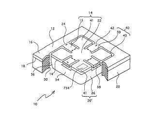
The flexure transducer element of the present invention
comprises a frame 12 and a sheet member 14. The frame 12
includes an upper surface 16 and a lower surface 18, and the
lower surface 18 is supported by a support member 20. The
sheet member 14 is substantially composed of flexible parts
10 15, center part 22 and weight upper part 41, and the flexible
part 15 extends outward from the center part 22 and is
integrally connected to the inner edge 24 (shown with the
broken line in Fig. 1) c~f the frame 12. The center part 22
of the sheet member 14 :includes the weight body 26 below it,
and the weight body 26 :is connected integrally to the center
part 22 through the neclc part 28 (see Fig. 3 (i)). In the
embodiment shown, the wESight body 26 includes the weight
upper part 41 thereon, <~nd these together substantially
constitute the weight 26' of the element.
The inward side surface 30 of the support member 20
opposes the outward side' surface 34 of the weight 26 through
the first space (or gap) 36. Further, the second space (or
gap) 38 is located between the flexible parts 15 and the
weight body 26, and the space is connected to the first
space. In addition, the space 39 is located between the
weight upper part 41 and the flexible part 15, the space 43
is located between the fmame 12 and the weight upper part 41,
and these spaces constitute the third space (or gap) 40. The
sheet member 14, particularly the flexible part 15 includes
on its surface, a plurality of piezoresistors 42 (not shown
in Fig. 2) and wires which are connected to the
piezoresistors (not shown). It is noted that the space 43
and the first space 36 are connected to each other so as to
CA 02251957 2001-07-25
32
constitute a slit form, and the second space 38 is connected
to the first space 36 and the third space 40 and thus these
spaces form a single space.
Fig. 3 shows the sequence of the production method of
the element 10 shown in Figs. 1 and 2 in cross sectional
views taken along the line B-B'.
Fig. 3 (a): First, a single crystal silicon substrate
50 is prepared as the semiconductor substrate of conductivity
type N. When an element (having a size of, for example,
5 mm x 5 mm) is produced, a plurality of elements (for
example 200-300 elements) are actually produced which are
integrally adjacent to o:ne another (in such a manner that the
elements are arranged one on the other and one next to the
other when viewing the substrate from above) using a circular
substrate (having a diameter of, for example, four inches)
followed by cutting and dividing them into each single
element using a dicing saw, which is generally known in the
semiconductor element art. Although the element and its
production method are explained with reference to a single
element for ease of understanding, it is obvious for those
skilled in the art that such explanations are applicable to
the production of a plurality of the elements. Therefore,
the substrate may be in a generally rectangular form or a
square form in the sense' of the production of the single
element.
Fig. 3 (b): Next, four sacrificial layers 56 each in
the form of a substantia7.ly elongated rectangle are formed in
the first main surface 58 of the substrate 50 which layers
extend from the four sides 52 of the rectangular or square
center part 23 of the silicon substrate 50 toward the outer
periphery of the substrate, but terminate at the positions 54
before the periphery. The formation of the sacrificial
layers is carried out under the consideration that the
flexible parts 15 are formed on the sacrificial layers,
masking all of the first main surface except those portions
CA 02251957 2001-07-25
33
on which the sacrificial layers are to be formed and then by
ion implantation of a P-type impurity such as boron into the
non-masked portions at a high impurity concentration followed
by annealing, so that those portions are formed with high
P-type impurity concentration. In this step, the sacrificial
layer 56 preferably has a width which is a little wider than
that of the flexible part 15.
Fig. 3 (c): Then, the epitaxial layer 60 of N type
conductivity is formed on the whole of the main surface 58 of
the substrate 50. Since the epitaxial layer 60 finally
constitutes the sheet member 14 (and also the frame 12), it
has such a thickness than the flexible part 15 is elastically
flexed and deformed where an acceleration is applied.
Thereafter, the P-type impurity is introduced (for example,
the impurity such as boron is diffused) into those portions
which correspond to the third space, so that those portions
62 are formed which haves the higher impurity concentration.
Fig. 3 (d): Then, t:he piezoresistors 64 and 66 which
transduce their resistance change due to the flexure into an
electric signal are formed on portions of the epitaxial layer
60 which are formed into the flexible parts which can flex
when the acceleration is applied. They are formed by
diffusing into such portions, the P-type impurity such as
boron of which conductivity type is opposite to that of the
epitaxial layer 60. It i.s noted that the piezoresistor 66
may be used for offset or used as one of the piezoresistors
which forms a bridge circuit.
Fig. 3 (e): Then, the wiring parts 68 which are
electrically connected to the piezoresistors 64 and 66 are
formed by the deposition and the thermal diffusion or the ion
implantation and the annealing treatment.
Fig. 3 (f): Then, the exposed surface of the epitaxial
layer 60 and the second main surface of the substrate are
covered with silicon nitride films 70. Thereafter, the
silicon nitride film is removed from that portion which
CA 02251957 2001-07-25
34
corresponds to an opening 72 of the first space 36 in order
to form the first space. It is preferable that silicon oxide
films are formed before the formation of the silicon nitride
films 70.
Fig. 3 (g): Then, by using an alkaline solution such as
a potassium hydroxide solution through the opening 72 on the
second main surface of the silicon substrate 50, the silicon
substrate 50 is partially removed by anisotropic etching so
that the first space 36 which leads to the sacrificial layer
56, the side surface 30 of the support member 20 and the side
surface 34 of the weight 26 are formed. The anisotropic
etching is such that et~~hing speed is faster along the
thickness direction of l.he silicon substrate 50 and slower
along a direction perpendicular to the thickness direction.
Thus, since the sacrificial layer 56 extends perpendicular to
the thickness direction of the silicon substrate 50, the
etching stops while the sacrificial layer is hardly etched.
Fig. 3 (h): Then, a portion of the silicon nitride
film 70 on the first main surface is removed, and the
electrode 74 is formed by the deposition or sputtering which
is electrically connected to the piezoresistor 64 or 66
through the wiring part E>8.
Fig. 3 (i): Then, the sacrificial layer 56 is removed
by the isotropic etching in which the etching proceeds in all
directions and an etchant: is supplied through the first
space 36, so that the sheet member 14 is formed from the
epitaxial layer 60 in wh.i.ch member both edges are supported
by the frame 12 of the epitaxial layer 60 and the weight 26
is hung from the center part 22 of the sheet member through
the neck part 28.
In the etching in this step, an acidic solution
containing hydrofluoric acid may be used. When such isotropic
etching is carried out, the etching speed is faster in the
sacrificial layer 56 in which the :impurity concentration is
high than in the epitaxial layer 60 in which the impurity
CA 02251957 2001-07-25
concentration is low, and thus, only the sacrificial layer 56
is selectively removed, whereby the second space is provided.
Finally, the portions 62 which have been so formed in the
step of Fig. 3 (c) that the impurity concentration thereof is
5 high are removed by the isotropic etching subsequent to the
removal of the sacrificial layer 56, so that the third space
is formed which is defined by the sheet member 14 and the
frame 12. The third space 40 may be in the form of a slit
composed of the spaces 39 and 43 as in the embodiment shown
10 in Fig. 1.
It is noted that differently from the RIE (reactive ion
etching), an edge portion includes a round corner when the
isotropic etching is used, thus stress concentration is
prevented at the edge wizen flexure is converged near the
15 edge, and thus there is an advantage in that a semiconductor
acceleration sensor is provided with an extended life time.
It is of course possibles to form the third space 40 using the
anisotropic etching which engraves along one direction or the
RIE when the round portion is not required.
20 In the above method according to the present invention,
since the anisotropic etching is used for the formation of
the first space, the distance between the side surfaces of
the support member and the weight can be made as small as
possible. That is, the first space can be made thin, and
25 also the first space can be located as outward as possible
with respect to the substrate, so that the volume of the
weight can be larger when a substrate having a fixed size is
used (thus, the weight can be heavier). Further, since the
sacrificial layer is formed and then removed, the connection
30 between the weight and the sheet member by the narrow neck
part, and thereby the distance can be longer from the center
of the flexible part to the frame when the substrate having a
fixed size is used. Particularly, when the flexible part is
substantially in the form of a beam as shown in Fig. 1, since
35 in addition to the flexure concentration in the flexible
CA 02251957 2001-07-25
36
part, the length of the flexible part can be longer, the
sensitivity of the sensor is improved.
In the shown embodiment, that portion of the epitaxial
layer except the center part 22 of the cruciform sheet member
14 and the weight upper part 41 includes no substrate below
it and is made of only the epitaxial layer 60, and thus such
a portion can substantially deform (or flex) when the
acceleration is applied..
The operation of the semiconductor acceleration sensor
shown in Fig. 1 will be explained. When an acceleration is
applied to the frame 12, the weight 26' is displaced toward a
direction which is oppo:>ite to the direction of the
acceleration application, so that the flexible part 15 of the
sheet member 14 flexes, thereby the piezoresistor 42 (or 64)
formed in that part flexes and its resistance changes. In
this case, that portion of the sheet member 14 which is
substantially elastically flexible is a both-end supported
beam structure in which both ends are supported by the frame
and the weight is connected to the center of the structure,
and the weight is supported by the four beams (flexible
parts 15). Therefore, the beams flex upon the acceleration
application along any direction with respect to X, Y and Z
axes which intersect with one another at a right angle, and
the acceleration including the three axis components can be
sensed.
The other piezoresistor 66 having the same structure as
that of the piezoresistor~ 64 is formed on the top surface of
the frame 12 as described above, and piezoresistors 64 and 66
are connected to each other so as to form a bridging circuit
(not shown). By measuring a resistance of the piezoresistor
64 through the circuit, the acceleration is detected which is
composed of the three axis components.
In the production method for the semiconductor
acceleration sensor as described above, the side surface 34
of the weight 26 is formed by anisotropically etching the
CA 02251957 2001-07-25
37
silicon substrate 50 from its second main surface, the sheet
member 14 is formed by isotropically etching and removing the
sacrificial layer 56 which is so formed that it partially
surrounds the center part 22 of the silicon substrate 50, and
such isotropic etching does not proceed as to the epitaxial
layer 60 which is formed into the sheet member 14 because of
the low impurity concentration of the epitaxial layer 60.
Therefore, the thickness of the sheet member 14 is precisely
controlled so that the <acceleration sensor having the both-
end supported beam structure is stably produced which has
less sensitivity dispersion.
In addition, although in the shown embodiment, the
actually elastically def=ormable portion is in the beam form,
it may be wider and/or :shorter when the sensitivity is not so
important.
Further, the conductivity type of the substrate and the
epitaxial layer 60 is an N-type in the above embodiment, it
may be a P-type, in which case the piezoresistor 64 may be of
an N-type.
Next, an embodiment will be explained in which the
removal of the sacrificial layer with etching is carried out
by etching and removing the sacrificial layer through the
third space so as to form the second space. The formation of
the third space may be carried out at any appropriate time,
and for example, it may be before or after, or simultaneously
with the formation of the first space.
First, the predetermined sacrificial layer 88 and the
epitaxial layer 82 are provided to the substrate 96 similarly
to Figs. 3 (a) to (c). 'then, as shown in Fig. 4 (a), the
epitaxial layer 82 is so masked that only the portion 84 of
the epitaxial layer 82 excluding portions which are to be
finally the sheet member 80 (including the center part 92 and
the flexible parts 106) and the frame 90 is subjected to the
etching, and then the portion 84 is removed by the RIE or the
anisotropic etching so that the third space 86 is formed as
CA 02251957 2001-07-25
38
an etchant introduction. port and the sacrificial layer 88 is
exposed at the bottom of the space 86, as shown in
Fig. 4 (b). Thereafter the sacrificial layer 88 is removed
by wet isotropic etching so that the sheet member 80 and the
frame 90 are formed and also the weight 94 including the neck
part 93 and the support member 95 are formed as shown in
Fig. 4 (c). In this way, when the etchant introduction port
is formed in the portion of the epitaxial layer excluding the
portions which are to be the sheet member and the frame, the
sacrificial layer 88 as the high impurity concentration layer
is directly etched, and also since the etching proceeds along
the direction shown with the arrow of Fig. 4 (b) below the
elongated portion of the=_ sheet member (i.e. the flexible
part 106), the etching path is shortened, which results in
the shorter etching removal period. In the absence of the
etchant introduction port, the etching proceeds along a
direction which is perpendicular to the arrow and from the
outer periphery of the weight 94 toward the neck part 93. It
is noted that the embodiment shown in Fig. 4, the first space
has been already formed..
In the embodiment shown in Fig. 4, the cross section of
the third space 86 alone the epitaxial layer 82 is of a
substantially square shape except that a corner portion 97
near the center part 92 is inwardly convex. The cross section
may be of any appropriate shape. Examples of the shape are
schematically shown in the top views in Figs. 5 (a) to (1).
Further additional examples are schematically shown in the
partially cut-away pers~~ective views in Figs. 6 (a) and (b).
For example, the etchant introduction port 86 (indicated
with the slanted lines) i.s formed by etching and removing the
epitaxial layer 82 except. those portions which are to be the
sheet member 80 and the frame 90, and then the etchant is
supplied through the port. 86 so as to etch and remove the
sacrificial layer 86. Then, a residence phenomenon of the
etchant is deleted so that the convection of the etchant
CA 02251957 2001-07-25
39
proceeds fast, and thereby that effect is advantageously
avoided which is based on the change of etchant composition
due to the self-catalytic decomposition of nitric acid
contained in the etchant in a locally confined space. Thus,
the sheet member 80 is :precisely formed without degrading the
selectivity of the sacrificial layer 88 over the epitaxial
layer 82. Further, as to the etching of the sacrificial
layer 88 below the flexible part 106, the etching can proceed
along the direction (i.e. the direction of the arrow shown in
Fig. 4 (b) or Fig. 6 (b,1) which is perpendicular to the
longitudinal direction :L04 of the flexible part 106, the
etching period can be shortened compared with the etching
along the longitudinal direction 104 of the flexible part
106. It is noted that t:he etchant introduction port 86 is
formed simultaneously with the formation of the first space
100 with the anisotropic: etching, the introduction port 86 is
produced without an additional step.
Figs. 5 (b) to (1) are schematic plane views of the
sensors for the semiconductor acceleration sensor according
to the present invention when viewing from above, and show
the shapes and the arrangements of the etchant introduction
ports.
In Fig. 5 (b), the corners of the shape of the etchant
introduction port 86 shown in Fig. 5 (a) when viewing from
above are rounded, which. improves the mechanical strength
against the stress concentration of the flexible part 106 of
the sheet member in the form of the beam at the end of the
part 106 which reaches the frame 90.
In Fig. 5 (c), the etchant introduction ports as shown
in Fig. 5 (a) are formed in only those portions which are
adjacent to the flexible parts 106. In this embodiment, the
sacrificial layer 13 is etched and removed below and near the
flexible parts 106, and the epitaxial portions 108 (which is
enclosed by the etchant introduction port 86 and the
frame 90) is not removed so that the substrate is left below
CA 02251957 2001-07-25
the portions when the sacrificial layer is absent, thereby
the sensitivity is improved because of the volume increase of
the weight. It is noted that it is required to form slits at
least partially inside 'the flexible parts 106 and between the
5 portions 108 and the fr;~me 90 using, for example, the RIE so
that the flexible parts 106 have additional flexibility.
In Fig. 5 (d), the etchant introduction ports 86 shown in
Fig. 5 (c) is divided into a plurality of the rectangular
portions, and the similar effect to that in the embodiment of
10 Fig. 5 (c) is achieved. The flexible parts 106 are partially
connected to the epitax:ial layer portions 108 which are
connected to the frame 90. When a. wafer is rotated at a high
speed upon coating with a resist, the flexure or breakage of
the sheet member 80, because of, for example, the high
15 viscosity of the resist,, is prevented, so that this
embodiment is better in the mechanical strength as to the
handling aspect (i.e. workability). As in the embodiment of
Fig. 5 (c), the slits ar_e required to be formed in the
flexible parts 106 so as to confer the additional
20 flexibility. In the shown embodiment, a plurality of the
rectangular etchant introduction ports 86 are formed.
However, there is no specific limitation to this, and, for
example, the etchant introduction port may be an oval shape.
Figs. 5 (e) to (h) correspond to the embodiments of
25 Figs. 5 (a) to (d) respe~r_tively in which the etchant
introduction ports 110 are further formed inside the flexible
parts 106, and thereby t:he sacrificial layer 88 is etched
from the center portions and the sides of the flexible parts
106 so that the etching period is shortened. The shape of
30 the etchant introduction port when viewing from above may be
any shape such as a circle, oval, rectangle, square, square
having round corners and so on, but the circle, the oval and
the square having the round corners are preferable when the
stress concentration around the etchant introduction port is
35 considered. A pluralit~~ of etchant introduction ports 110
CA 02251957 2001-07-25
41.
may be present along a centerline of the flexible part 106
which is parallel to the longitudinal direction of the
flexible part. It is noted that the above descriptions as to
Fig. 5 (a) to (d) are also applicable to Fig. 5 (e) to (h)
respectively when they are appropriate.
Figs. 5 (i) to (1) correspond to the embodiments of
Figs. 5 (a) to (d) respectively in which the etchant
introduction ports 112 are further formed along substantially
the entire length of the flexible parts 106, and thereby the
sacrificial layer 88 is etched from the center portion and
the sides of the flexible part 106 along a direction
perpendicular to the longitudinal length of the flexible part
106 so that the etching period is shortened. The shape of
the etchant introduction port 112 when viewing from above may
be any shape such as an oval, rectangle, square, rectangular
having four round corners and so on, but the oval and the
rectangular having the four round corners are preferable when
the stress concentration around the etchant introduction port
is considered. It is noted that the above descriptions as to
Fig. 5 (a) to (d) are also applicable to Fig. 5 (i) to (1)
respectively when they are appropriate.
In the embodiments shown i.n Fig. 5 (a), Fig. 5 (b),
Fig. 5 (e) , Fig. 5 (f) , Fig. 5 (i) and Fig. 5 (j ) , the
epitaxial layer 82 is removed by etching except the sheet
member 80 and the frame 90 as in the embodiment shown in
Fig. 6 (b). However, in the embodiments shown in Fig. o (c),
Fig. 5 (d), Fig. 5 (g), Fig. 5 (h), Fig. 5 (k) and
Fig. 5 (1), the epitaxial layer 82 may be etched in only
those portions which are adjacent to the frame 90 so that the
slit 87 is formed and is connected to the first space and the
third space, as shown in Fig. 6 (a), so that the weight 94 is
made heavier and thereby the sensitivity is improved. The
flexible parts 106 of the embodiments shown in Figs. 5 (e) to
CA 02251957 2001-07-25
42
(1) correspond to the flexible parts 106 of Fig. 6 (a) in
which the etchant introduction ports 110 or 112 are further
formed.
In the embodiments shown in Fig. 5 (c), Fig. 5 (d),
Fig. 5 (g) , Fig. 5 (h), Fig. 5 (k) and Fig. 5 (1), if a size
of the etchant introduction port 86 (especially the size of
the portion 84) is so designed under the consideration of the
anisotropic etching properties that the etching automatically
stops when the sacrificial layer 86 is reached, excessively-
etching of the weight 94 is prevented, which otherwise would
reduce the sensitivity. Such designing can be carried out by
controlling an opening size of the mask for the anisotropic
etching.
In the embodiments shown in Figs. 5 and 6, although the
weight is carried by the four flexible parts 106 in the form
of the beams (see Fig. 6 (a)) or the eight flexible parts 106
in the form of the beams (see Fig. 6 (b)), the number of
beams is not limited to such embodiments. Any number (for
example, twelve beams and sixteen beams) of beams may be
employed to carry the weight.
In the embodiment shown in Fig. 6 (a), the epitaxial
layer 82 forms the sheet member 80 including the flexible
parts 106, the center :part 107 and weight upper parts 91,
while the embodiment shown in Fig. 6 (b) has no weight upper
parts.
The formation of the third space by providing the second
high impurity concentration layer in the epitaxial layer will
be explained with reference to Fig. 7.
Fig. 7 schematically shows in the cross sectional views,
the steps for the production of the transducer element for
the semiconductor acceleration sensor according to the
present invention, and Fig. 8 schematically shows in the
partially cut-away perspective views, some stages during the
steps of Figs . 7 (b) to ( i ) .
CA 02251957 2001-07-25
43
Fig. 7 (a): On the single crystal silicon substrate 150
as an N-type semiconductor substrate having a thickness of,
for example, 400 to 600 ~m and an orientation of the crystal
plane (crystal orientation) of (100) is provided a silicon
oxide film 152 by, for example, thermal oxidation, and then
the openings 154 are formed by etching the silicon oxide film
152 through a mask of a photoresist (not shown) having a
predetermined pattern followed by 'the removal of the
photoresist through, for example, the plasma ashing. The
openings 154 are formed on those portions which extend
outward from four sides surrounding the generally rectangular
center part 156 (thus, the portions are elongated ones which
partly surround the center part), and on which the flexible
parts (concretely, the beam parts) are to be formed, and also
on vicinities along longitudinal directions of those
portions. Thus, the width of the flexible part 158 is
smaller than that of the opening 154.
The opening 154 is not limited to the shown embodiment,
and it may be formed in that portion which entirely surrounds
the center part 156 of the single crystal silicon substrate
150 (i.e. that portion is annular).
Then, using the silicon oxide film 152 having the
openings 154 as the mask, the sacrificial layers 160 are
formed as high impurity concentration layers in which the
P-type impurity such as boron (B) is present at a high
concentration by the deposition and the thermal diffusion or
the ion implantation and the annealing treatment of the
P-type impurity. The concentration of the P-type impurity in
the sacrificial layer 160 is desirably, for example, not less
than 1.0 x 101' cm~3 and below its solid solubility (limi.t).
Fig. 7 (b): Then, the silicon oxide film 152 is removed
by etching. Thereafter, on the side where the P-type
sacrificial layer 160 of the single crystal silicon substrate
150 is formed there is formed the epitaxial layer 162 which
has a thickness such that the flexible part 158 to be formed
CA 02251957 2001-07-25
44
can elastically flex when the acceleration is applied, and
then the piezoresistors 164 are formed in the predetermined
portions of the corresponding flexible parts 158 of the
epitaxial layer 162 using a resist having the predetermined
pattern as a mask and also using the deposition and the
thermal diffusion or the ion implantation and the annealing
treatment of the P-type impurity such as boron (B) (see
Fig. 8 (a) ) .
Fig. 7 (c): Similarly, the diffusion wirings 166 are
formed which are electrically connected to the piezoresistors
164 by the deposition and the thermal diffusion or the ion
implantation and the annealing treatment of the P-type
impurity, and then the photoresist is removed.
Fig. 7 (d): Then, the P-type impurity layers 168 which
reach the buried P-type impurity layer 162 are formed
adjacent to those portions which are to be the sheet member
of the epitaxial layer 162, especially the flexible parts 158
by the deposition and the thermal diffusion or the ion
implantation and the annealing treatment of the P-type
impurity, and then the photoresist is removed (see
Fig. 8 (b)).
In this embodiment, the impurity layers 168 are formed
adjacent to the f:Lexib:le parts 158, to which the embodiment
is not limited. The impurity layers of the epitaxial layer
may be formed so that they are connected to the sacrificial
layer 160 excluding the flexible parts 158, the center part
188 and frame 186. Further, in this embodiment, although the
impurity layers 168 are formed after the piezoresistors 164
and the diffusion wirings 166 have been formed, the
piezoresistors 164 and the diffusion wirings 166 may be
formed after the impurity layers 168 have been formed.
Fig. 7 (e): Then, on the single crystal silicon
substrate 150 and the epitaxial layer 162 are formed the
silicon oxide films 170, on which protection films 172 such
as silicon nitride films are formed. These two kinds of
CA 02251957 2001-07-25
films are advantageous in that their camber directions are
opposite to each other, which serves to keep the substrate
flat. Thereafter, the openings 176 are formed in
predetermined portions which correspond to the outer
5 periphery of the weight 174 described below by etching the
silicon oxide film 170 and the protection film 172 thereon
using the photoresist (not shown) as a mask having the
predetermined pattern, and then the resist is removed.
Fig. 7 (f): Then, the silicon substrate 150 is
10 anisotropically etched with an alkaline etchant solution
(such as a KOH solution) using as a mask the protection film
172 having the openings 176, so that the first space 178
reaching the buried P-type sacrificial layer 160 is formed.
Fig. 7 (g): Then, portions of the silicon oxide film
15 170 and the protective film 172 on the P-type impurity layers
168 are removed by etching so as to provide openings (not
shown) which are used for the formation of the third space,
and through which an etchant based on hydrofluoric
acid/nitric acid is supplied to form the etchant introduction
20 ports 180 as the third space.
Fig. 7 (h): Then, through the etchant introducti0I1
ports 180 is supplied an etchant based on hydrofluoric
acid/nitric acid so that the buried P-type sacrificial layers
160 are removed to form the second space 182 (see
25 Fig. 8 (c)). As the etchant based on hydrofluoric
acid/nitric acid herein, an etchant containing hydrofluoric
acid . nitric acid . acetic acid = 1 . 1 to 3 . 8 (50%
hydrofluoric acid aqueous solution: 69% nitric acid aqueous
solution . acetic acid, based on volume) may be used.
30 It is noted that the etching of the sacrificial layer
160 may be carried out through the first space 178 and the
third space 180.
Fig. 7 (i): Then, the predetermined portions of the
silicon oxide film 170 and the protection film 172 thereon
35 which portions are on the diffusion wirings 166 are removed
CA 02251957 2001-07-25
46
by etching so as to provide contact holes which are filled,
and then metal (such as aluminum) wirings 184 are so formed
that they are electrically connected to the piezoresistors
164 through the diffusion wirings 166, and thereafter, the
silicon oxide film 170 on the silicon substrate 150 and the
protection film 172 thereon are removed by etching (see
Fig. 8 (d)).
Finally, those portions of the epitaxial layer 162 which
exclude portions to be the flexible parts 158, the center
part 188 and the frame 186, and optionally a portion of the
single crystal silicon substrate 150 below them are removed
by the RIE (reactive ion etching), whereby the sheet member
(158 + 188) of which all ends are supported by the frame, and
the weight 174 is hung from the center part 188 is provided,
resulting in the element according to the present invention
(see Fig. 8 (e)). In the element, the interfaces between the
flexible parts 158 and the frame 186 as well as the
interfaces between the flexible parts 158 and the center part
188 are preferably processed so as to have the edges with the
rounded corners (or sides) thus avoiding stress
concentration.
In this embodiment, the etchant introduction ports 180
are formed in those portions which are adjacent to the
flexible parts 158 of the epitaxial layer in the form of the
beams, and the etchant is supplied to such ports to remove
the buried P-type sacrificial layer 160 by etching. This
avoids the effect based on the change of the etchant
composition due to the self-catalytic decomposition of nitric
acid contained in the etchant in the locally confined space.
Thus, the flexible parts 158 are precisely formed without
degrading the selectivity of the buried P-type sacrificial
layer 160 over the epitaxial layer 162.
CA 02251957 2001-07-25
47
Also, since the P-type impurity layer 168 is of the same
high impurity concentration as the P-type impurity layer 160,
the etching removal of the impurity layers 168 and 160 can be
carried out successively, so that the step can be shortened.
Further, in this embodiment, since the etching can be
carried out not along the longitudinal direction of the
flexible part 158, but. along a direction which is
perpendicular to the longitudinal direction of the flexible
part 158, the etching path can be shortened.
Next, an embodiment will be explained wherein the .first
space is composed of two parts.
Fig. 9 shows a schematic cross sectional view of one
embodiment of the element 200 for the semiconductor
acceleration sensor according to the present invention, and
is substantially similar to, for example, the cross sectional
view of Fig. 3 (i) except that the shape (or form) of the
first space 202 is different.
As can be easily seen from Fig. 9, the element 200
includes the first space 202 composed of the first part 204
which is formed by a mechanical or chemical process and the
second part 206 which is formed by the anisotropic etching.
Clearly from Fig. 9, the side surface 210 of the weight 208
and the side surface 214 of the support member 212 form a
taper such that the angle (81) of the first part is smaller
than the angle (Az) of the second part, each angle being
defined by the tow side surfaces.
Upon the formation of the first space 202, when the
anisotropic etching is used from the beginning of the
formation, the angle formed by the side surface of the weight
and the support member is A2, and the etching has to proceed
up to such a depth that the sacrificial layer is reached.
Thus, the opening 216 should be larger as shown with broken
lines, so that there occurs a problem that the volume of the
weight is decreased. Such a problem is overcome in this
embodiment.
CA 02251957 2001-07-25
48
That is, in the element as shown, the volume of the
weight can be increased without enlarging an area of the
opening 216 for the first space. This means that the
sensitivity of the acceleration sensor can be improved
without enlarging the chip area of the sensor. It is noted
that although in the embodiment shown, the first space is
composed of the two parts, the first part may be ground
mechanically or chemically so as to further divide it into a
plurality of sub-parts provided that the tapering angle of
the sub-part is smaller than the tapering angle of the second
part (82) .
Concretely, upon the formation of the first space as
above, the semiconductor substrate 218 is mechanically ground
up to around its midpoint so as to form the first part :?04.
The shape of the opening of the first part 204, especially
the distance between both side surfaces should be such that a
sufficient second part opening is ensured for the formation
of the second part 206 in the next step.
As to the mechanically grinding for the formation of the
first part, for example, using a dicing saw or collision of
particles at a high speed (such as sandblast manner) may be
used. The sandblast manner blows fine sand particles against
an object at a high pressure and thereby surface material is
removed from the object. Alternatively, the first part may
be formed using a chemical reaction, and for example,
reactive ion etching (RIE) may be used.
Then, the second part 206 is formed by the anisotropic
etching using an alkaline solution such as a potassium
hydroxide aqueous solution. The etching is carried out so
that when the sacrificial layer is present in the second
space 220, it proceeds up to the sacrificial layer which
serves as an etching stop layer. When the sacrificial layer
is not present, the etching is stopped when it reaches 'the
second space 220. The first part 204 functions as a mask and
an etchant introduction port for the formation of the second
CA 02251957 2001-07-25
49
part 206. As the etchant, in addition to the potassium
hydroxide aqueous solution, ethylenediamine pyrocatechol,
hydrazine and so on may be used.
Mechanical grinding is advantageous in that the removal
speed is larger compared with the etching so that a thicker
substrate can be worked, which makes the volume (thus heft)
of the weight larger. The reactive ion etching is one of the
semiconductor processing techniques, and advantageous in that
it is used in the same environment as used in other
processing for the production of the element, and also that 81
can be smaller relative to the mechanical grinding (namely,
grinding can be carried out at an angle which is closer to a
right angle with respect to the substrate 218), so that the
opening 216 is made smaller and A1 can be substantially 0°.
The embodiment wherein the first space is made of the
two parts will be explained in detail with reference to
Fig. 10.
Fig. 10 (a): As the semiconductor substrate 218, an
N-type substrate having a crystal plane orientation of (:100)
is used. The semiconductor substrate 218 desirably has an
impurity concentration of not more than 1.0 x 101' cm-3. The
thickness of the substrate is a little thicker (for example,
a thickness of about 1000 um) relative to the conventionally
used one.
First, in a diffusion step for the formation of the
sacrificial layer 230, the deposition and the thermal
diffusion or the ion implantation and the annealing treatment
are carried out. The impurity such as boron is used herein
and doped to a high concentration. The diffusion depth is
controlled depending on the application. The sacrificial
layer 230 may be an N-type high impurity concentration layer
while using antimony, phosphorous and so on. The sacrificial
layer 230 functions as an etching stop and the sacrificial
layer itself in the present invention.
CA 02251957 2001-07-25
Fig. 10 (b): The epitaxial layer 232 is formed on the
substrate 218 through the epitaxial growth. The epitaxial
layer 232 constitutes the frame and the sheet member of the
flexure transducer element. Since the layer 232 is formed by
5 the epitaxial growth, its thickness is controlled easily and
precisely.
Fig. 10 (c): Then, the piezoresistors 234 are formed in
those portions of the epitaxial layer which are to become the
flexible parts by the thermal diffusion or the ion
10 implantation and the annealing treatment using the P-type
impurity such as boron.
Fig. 10 (d): Then, the diffusion wirings 236 which
output the change of resistance of the piezoresistors 234 are
formed in those portions of the epitaxial layer 232 which are
15 to become the flexible parts by the deposition and the
thermal diffusion or the ion implantation and the annealing
treatment using the P-type impurity such as boron. The
impurity concentration is larger than that in the
piezoresistor formation step (Fig. 10 (c)).
20 Fig 10 (e): Then, the protection mask 238 which protects
the epitaxial layer 232, the piezoresistors 234 and the
diffusion wirings 236 as well as the formation mask 240 which
is used to form the weight 250 are farmed. Both masks are
preferably made of a silicon nitride film and/or a silicon
25 oxide film. Subsequently, the first part 242 is formed by
mechanically grinding the semiconductor substrate 218, for
example, up to around the midpoint thereof. As the
mechanical grinding means, a dicing saw is used. The size of
the opening 244 of the first part 242 is such that the
30 necessary opening 245 is ensured far the next step for the
production of the second part 246.
Fig. 10 (f): Then, the second part 246 is formed by
anisotropically etching using the alkaline aqueous solution
such as a potassium hydroxide. The etching is carried out up
35 to the sacrificial layer 230 which functions as the etching
CA 02251957 2001-07-25
51
stop layer. The first part 242 functions as an etching mask
and an etching solution introduction port for the formation
of the second part 246.
Fig. 10 (g): Then, the predetermined portions of the
silicon oxide film and t:he silicon nitride film on the-
diffusion wirings are removed so as to form contact holes,
and the metal wirings 248 are so formed that they are in
contact with the diffusion wirings 236 by sputtering or
deposition. When aluminum is used, a thermal treatment such
as sintering is desirab7_y carried out. For the metal wirings
248, gold, chromium and 50 on may be used.
Fig. 10 (h): Finally the sacrificial layer 230 which has
functioned as the etching stop layer is removed by etching so
as to form the second space 254. For the etching herein, for
example, a solution containing hydrofluoric acid . nitric
acid . acetic acid = 1 . 1 to 3 . 8 is used. In this case,
since the etching speed in the low impurity concentration
(diffusion) layer having an impurity concentration not larger
than 1.0 x 101' cm-3, is reduced to about 1/150 of the etching
speed of the diffusion layer having an impurity concentration
above 1.0 x 101' cm-3 only the low impurity concentration
(diffusion) layer can be selectively left. That is, the
sacrificial layer 230 in which the impurity is diffused at a
high concentration can be selectively etched so that the
weight 250 and the support member 252 is separated.
When as described above, the first space is divided into
the plural parts, for example two parts and the anisotropic
etching is applied for the final part while the mechanical
grinding or the RIE is applied for the other parts so that
those parts are formed, the volume of the weight 250 can be
made large without enlarging the area of the opening 244,
whereby the sensitivity of the acceleration sensor can be
improved without enlarging a chip area.
Then, an embodiment in which the wiring protection film
is formed in the production of the acceleration sensor will
CA 02251957 2001-07-25
52
be explained with reference to Fig. 11 which schematically
shows the production steps of the acceleration sensor.
Fig. 11 (a): On the single crystal silicon substrate 300
as an N-type semiconductor substrate having a thickness of
for example 400 to 600 hem and a crystal plane orientation of
(100) is provided a silicon oxide film 302 by, for example,
the thermal oxidation, and then the openings 304 are formed
by etching the oxide film 302 with a mask of a photoresist
(not shown) having a predetermined pattern followed by the
removal of the photoresi.st through, for example, the plasma
ashing. The openings 304 are formed on those portions which
surround the generally rectangular center part 306 of the
single crystal silicon substrate 300.
Then, using the silicon oxide film 302 having the
openings 304 as the mask., the P-type sacrificial layers 308
are formed in which the P-type impurity such as boron (B) is
doped by the deposition and the thermal diffusion or the ion
implantation and the annealing treatment of the P-type
impurity. It is noted that in place of the silicon oxide
film, for example a silicon nitride film is formed, and then
the deposition and the thermal diffusion or the ion
implantation and the annealing treatment may be carried out
using the nitride film as a mask.
Fig. 11 (b): Then, the silicon oxide film 302 is
removed by etching. Thereafter, on the side where the buried
P-type impurity sacrificial layer 308 is formed in the single
crystal silicon substrate 300 is formed the N-type epitaxial
layer 310, and then the piezoresistors 312 are formed in the
predetermined portions of the flexible parts 338 which are to
be formed from the epitaxial layer 310 using the deposition
and the thermal diffusion or the ion implantation and the
annealing treatment of the P-type impurity. It is noted that
since the epitaxial layer 310 is finally formed into the
CA 02251957 2001-07-25
53
sheet member including the flexible parts 338, it is formed
to have a thickness which allows the elastic flexure upon the
application of the acceleration.
Fig. 11 (c): Then, the diffusion wirings 314 are so
formed that they are electrically connected to the
piezoresistors 312 by the deposition and the thermal
diffusion or the ion implantation and the annealing treatment
for the high P-type impurity concentration, and then the
silicon oxide films 316 are formed on the single crystal
silicon substrate 300 and the exposed epitaxial layer 310.
Fig. 11 (d): Then, the protection films 318 such as
silicon nitride films a:re formed on the silicon oxide films
316 by, for example, tha_ CVD process, and then a portion of
the protection film 318 and the silicon oxide film 316 is
removed by etching, for example, the RIE, so that the opening
320 for the first space :322 is formed which surrounds the
weight 336 which will be explained below.
Fig. 11 (e): Then, the single crystal silicon substrate
300 is anisotropically etched using, as a mask, the
protection film 318 having the opening 320 and also using an
alkaline based etchant :such as a potassium hydroxide aqueous
solution, so that the first space 322 is formed which reaches
the P-type sacrificial layer 308.
Fig. 11 {f): Then, the predetermined portions of the
silicon oxide film 316 and the protection film 318 which are
on the diffusion wirings 314 are removed by etching, and then
the metal wirings 324 (made of for example aluminum) and the
electrode pads (not showra) are so formed that they are
electrically connected to the diffusion wirings 314, and then
the wiring protection film 326 such as a chromium film, a
silicon nitride film or a. fluoroplastic film is formed on the
side of the single crystal silicon substrate 300 having the
metal wirings 324.
It is noted that when the conventional aluminum is used
for the metal wirings 324, an alloy spike problem may occur
CA 02251957 2001-07-25
54
above 500°C. Therefore, it is desirable that the wiring
protection film 326 of t:he silicon nitride film is applied in
low temperature growth using, for example, the plasma CVD
method.
Fig. 11 (g): Then, portions of the wiring protection
film 326, the protection film 318, the silicon oxide film 316
and the epitaxial layer 310 are removed by the RIE, the
anisotropic etching or the isotropic etching, so that the
third spaces 328 including the etchant introduction port
which reach the buried F~-type sacrificial layer 308 are
formed. Then, the etchant of an acidic solution containing
hydrofluoric acid (hydrc>fluoric acid . nitric acid . acetic
acid = 1 . 1 to 3 . 8) i.s supplied through the etchant
introduction ports so a~; to isotropically etch and remove the
buried P-type sacrificial layer 308 and the second space 330
is formed, whereby the sheet member 338 is formed the ends of
which are connected to the frame 334 supported by the support
member 332 made of the ~;ubstrate 300 and made of the
epitaxial layer 310, anct the weight 336 is connected to the
center part thereof.
Fig. 11 (h): Then, the wiring protection film 326 as
well as those portions of the silicon oxide film 316 and the
protection film 318 which are on the side of the bottom
surface of the weight 338 are removed by etching. Finally,
the stopper (or the bottom cover) 342 which contains the
recess part 340 in a portion thereof corresponding to the
weight 336 is connected to the support member 332 by, for
example, anode bonding, which results in the acceleration
sensor according to the present invention.
Another embodiment in which the wiring protection film
is formed is shown in Fig. 12. Up to the formation of the
silicon oxide film 316, this embodiment is similar to
Fig. 11, and thus the explanation with respect to the
formation of the silicon. oxide film 316 is omitted.
CA 02251957 2001-07-25
Fig. 12 (a): Thereafter, the predetermined portions of
the silicon oxide film :316 which are on the diffusion wirings
314 are removed by etching, and then the metal wirings 324
(made of for example aluminum) and the electrode pads (not
5 shown) are so formed by,, for example, the sputtering or the
vapor deposition that they are electrically connected to the
diffusion wirings 314.
Fig. 12 (b): Then,, the wiring protection films 326 of
the silicon nitride films are formed on both silicon oxide
10 films 316 by, for example, the CVD, and then a portion of the
wiring protection film :326 and the silicon oxide film 316 is
removed by etching, for example, the RIE, so that the opening
320 for the first space 322 is formed. It is noted that the
wiring protection film :326 are so formed that it covers the
15 metal wirings 324 and the electrode pads (not shown).
Fig. 12 (c): Then,, the single crystal silicon substrate
300 is anisotropically etched using as a mask the wiring
protection film 326 having the opening 320, so that the first
space 322 is formed which reaches the sacrificial layer 308.
20 Fig. 12 (d): Then,, portions of the wiring protection
film 326, the silicon o:{ide film 316 and the epitaxial layer
310 are removed by etch_Lng, for example the RIE, the
isotropic etching or the' anisotropic etching so that the
third space 328 which reaches the sacrificial layer 308 is
25 formed. Through the th_Lrd space 328, the etchant comprising
an acidic solution which contains hydrofluoric acid and so on
(a solution containing hydrofluoric acid . nitric acid .
acetic acid = 1 . 1 to ;3 . 8) is supplied so as to remove the
sacrificial layer 308.
30 Fig. 12 (e): Fina=Lly, the wiring protection films 326
are removed, and then the stopper (or the bottom cover) 342
which contains the recess part 340 in a portion thereof
corresponding to the we_Lght 336 is connected to the support
member 332 by, for example, anodic bonding, which results in
35 the acceleration sensor according to the present invention.
CA 02251957 2001-07-25
56
It is noted that in the embodiment shown in Fig. 12, the
wiring protection films 326 are removed from the whole of the
surfaces, but the present invention is not limited to this
embodiment. Only those portions of the wiring protection
film 326 which are on tree electrode pads may be thinned
beforehand by pattern etching, and then the wiring protection
film 326 is etched over its entire surface to reduce the
thickness of the film 326 after the etching of the
sacrificial layer 308, :~a that only the electrode pads are
exposed. In this way, t:he other portions but the electrode
pads are covered by the silicon nitride film, which improves
the moisture resistance of the sensor element. The reasons
why the wiring protection film 326 on the electrode pads are
thinned beforehand by tree pattern etching are that the
substrate has irregularities on its surface after the etching
of the sacrificial layer 308 and also has less strength so
that a pattern processing (for example, a photolithography
step) becomes difficult, and that when the only portions of
the wiring protection film 326 on the electrode pads are
thinned beforehand by tree pattern etching, only the electrode
pads are exposed by etching the wiring protection film 326
over its entire surface without the pattern processing after
the etching removal of t:he sacrificial layer 308.
In a further embodiment, the first space 322 is partially
formed so that a portion 350 of the substrate is left between
the sacrificial layer 308 and the first space 322, then the
sacrificial layer is removed, and then the left portion 350
of the substrate is removed. In this embodiment, even after
the etching of the sacrificial layer 308, the weight 336 and
the support member 332 are not separated so that no breakage
of the substrate occurs in this step, which greatly improves
the yield of the substrate.
More concretely, such an embodiment will be explained
with reference to Fig. 7_3.
CA 02251957 2001-07-25
57
Fig. 13 (a): The first space 322 is formed by the
anisotropic etching using the etchant of an alkaline solution
such as a potassium hydroxide (KOH) solution. In this
instance, the etching is stopped before the first space 322
reaches the sacrificial layer 308 so that the portion 350 of
the single crystal silicon substrate having a thickness of,
for example, several tens of micrometers is left below the
sacrificial layer 308.
Fig. 13 (b): Then, the predetermined portions of the
silicon oxide film 316 a.nd the protection film 318 on the
diffusion wirings 314 are removed by etching, then the metal
wirings 324 (made of for' example aluminum) and the electrode
pads (not shown) are formed so that they are electrically
connected to the diffusian wirings 314, and then wiring
protection film 326 such as a chromium film, a silicon
nitride film or a fluoroplastic film is formed on the side of
the single crystal si:lican substrate 300 which side contains
the metal wirings 324.
Fig. 13 (c): Then, as in the embodiment shown in
Fig. 12, the third space 328 is formed, through which the
etchant of an acidic solution containing hydrofluoric acid is
then supplied so as to i.sotropically etch and remove the
sacrificial layer 308 and thereby the second space 330 is
formed. Then, the portion 350 of the single crystal silicon
substrate below the sacrificial layer 308 is removed by
etching, for example, the RIE or the anisotropic etching so
that the first space 322. is connected to the second space
330.
It is noted that the shape of the portion 350 of the
single crystal silicon ~;ubstrate which is left below the
buried sacrificial layer 308 after the etching depends on the
etching manner, and the anisotropic etching using an alkaline
etchant provides the larger tapering angle (81) of Fig. 9
compared with the RIB. Thus, when the area which the element
occupies is fixed, the RIE provides the larger size for the
CA 02251957 2001-07-25
58
weight. This also means that when the size of the weight is
fixed, the RIE provides the smaller chip compared with the
wet anisotropic etching.
In a further embodiment, after the silicon oxide film
316 and the protection film 318 on a bottom surface of a
portion which is to be the weight are removed by etching, the
single crystal silicon substrate portion 350 left below the
buried sacrificial layer 308 and the bottom surface of the
portion which is to be the weight bottom are removed by the
anisotropic etching using the alkaline etchant or the RIE
while using the protection film 318 on the support member 332
as a mask. In this embodiment, the thickness of the weight
336 is reduced, and the stopper 342 having a flat form is
connected to the support member 332 by, for example, anodic
bonding (see Fig. 13 (d)). In this way, no recess part has
to be formed in the stopper 342, which decreases the
processing cost of the stopper, thus reducing the overall
production cost of the chip.
An embodiment will now be explained in which the
concentration of the impurity in the surface of the
sacrificial layer is smaller than that of an inner side
thereof.
Fig. 14 shows a formation method for the buried
sacrificial layer having a desired final depth of 10 Vim.
Fig. 14 (a): First, a field oxide film 362 having a
thickness of about 12000 A is formed on the surface of the
N-type silicon substrate 360 by, for example, the thermal
oxidation. The oxide film is patterned as predetermined using
the photolithography and the etching so as to form the
openings 364.
Fig. 14 (b): Subsequently, using the field oxide film
362 as a mask, boron as the P-type impurity is deposited and
then thermally diffused in a nitrogen atmosphere at the
surface of the silicon substrate 360 so as to form the P-type
impurity high concentration layer 366 having a depth of about
CA 02251957 2001-07-25
59
~.m. Then, the silicon oxide film 368 having a thickness of
about 3500 A is formed _Ln the substrate surface in the
opening 364 by the wet oxidation or pyrogenic oxidation. For
example, while the impurity concentration at the surface of
5 the high P-type impurity concentration layer 366 in the case
of only the thermal difi_usion under the nitrogen atmosphere
is about 1 x 10²° cm-3, the concentration is reduced to about
4 x 1019 cm-3 when the additional wet oxidation or pyrogenic
oxidation is carried out..
Fig. 14 (c): Then, the field oxide film 362 and the
silicon oxide film 368 are fully removed by the wet etching
over the entire surface followed by the deposition of the
N-type epitaxial layer 370. At this stage, boron diffuses
into the epitaxial layer 370 through an interface with the
silicon substrate 360 and a final buried diffusion layer 372
is formed.
In this embodiment, when a silicon substrate having an
impurity concentration of, for example, 1 x 1015 cm-3, boron
diffuses into the epita}:ial layer 370 by about 4~.m to about
5 ~m without the wet oxidation or pyrogenic oxidation while
about 3.5 ~m with the wet oxidation or pyrogenic oxidation,
and also the thickness of inversion layer formed by the auto-
doping is about 5 ~m wit:hout the wet oxidation or pyrogenic
oxidation while being reduced to about 2.5 ~m with the wet
oxidation or pyrogenic oxidation. Further, the peak
concentration in the inversion layer is in the order of lOls
cm-3 without the wet oxidation or pyrogenic oxidation while
being reduced to about t:he order of 1015 cm-3 with the wet
oxidation or pyrogenic oxidation.
Fig. 15 shows another embodiment in which the
concentration of the impurity in the surface of the
sacrificial layer is smaller than that of the inner side
thereof.
Fig. 15 (a): First, a field oxide film 362 having a
thickness of about 5000 A is formed on the surface of the
CA 02251957 2001-07-25
N-type silicon substrate 360 by, for example, the thermal
oxidation. The oxide film is patterned as predetermined
using the photolithography and the etching so as to form the
openings 364.
5 Fig. 15 (b): Subsequently, using the field oxide film
362 as a mask, boron as the P-type impurity is ion implanted
in the surface of the silicon substrate 360.
Fig. 15 (c): By annealing under an oxygen atmosphere,
the silicon oxide film 365 and the high P-type impurity
10 concentration layer 366 below the film are formed.
It is known that a ,peak of an impurity profile along the
thickness direction just. after the ion implantation appears
in a portion which is a little in side of the implantation
surface due to the channeling effect. The peak position from
15 the surface is determined by the kind of impurity and
acceleration energy upon the implantation. For example, when
boron is ion-implanted with an acceleration energy of
100 keV, the peak appears at a point which is about 0.25 ~m
inside of the implantation surface. Considering a fixed peak
20 concentration, impurity concentration at the surface is lower
when the peak position is deeper. In the embodiment shown in
Fig. 15, anything such as a protection oxide film is not
formed on the surface of the opening 364 of the substrate,
and the silicon substrate 360 is exposed. Since the ion
25 implantation is carried out into such a surface, when
compared with the presence of, for example, the protection
film in the surface of the silicon substrate, the peak of the
impurity profile is located at a deeper position from the
surface and simultaneously the surface of the substrate has a
30 lower impurity concentration. Even when the diffusion toward
the inside of the substrate proceeds by the annealing
treatment thereafter, since the concentration profile is not
changed, only the surface P-type impurity concentration can
be suppressed while keeping an overall impurity concentration
35 in the high P-type impurity concentration layer 366 around
CA 02251957 2001-07-25
61
1.0 x 10²° cm-3 by properly selecting the ion-implantation
conditions and the anne<~ling treatment conditions thereafter.
It is noted that when the annealing treatment is carried
out under a nitrogen atmosphere, the sacrificial layer
remains exposed in the opening, but when the annealing
treatment is carried out. under an oxygen atmosphere, the
opening is covered with the silicon oxide film. Implanted
impurity is likely to e:~cape into the oxide film, so that the
impurity concentration ~_n the substrate surface is preferably
lower compared to the circumstance when the oxide film is
absent.
Fig. 15 (d): Then, the field oxide film 362 and the
silicon oxide film 365 are fully removed from the entire
surface of the substrate:, and then an N-type epitaxial layer
370 is deposited thereon. At this stage, boron diffuses into
the epitaxial layer 370 through the interface with silicon
substrate 360 so that tree final sacrificial layer 372 is
formed .
Fig. 16 shows a further formation method for the
sacrificial layer having a desired final depth of 10 ~.m.
Fig. 16 (a): First:, a field oxide film 362 having a
thickness of about 12000 A is formed on the surface of the
N-type silicon substrate' 360 by, for example, the thermal
oxidation. The oxide film is patterned as predetermined
using the photolithography and the etching so as to form the
openings 364.
Fig. 16 (b): Subsequently, using the field oxide film
362 as a mask, boron as the P-type impurity is deposited on
the surface of the silicon substrate 360 and then thermally
diffused in an oxygen atmosphere, and the silicon oxide film
365 in the opening 364 and the high impurity concentration
layer 363 below it are formed.
Fig. 16 (c): Similarly, using the field oxide film 362
as a mask, phosphorous as the N-type impurity is implanted.
CA 02251957 2001-07-25
62
Fig. 16 (d): By annealing treatment in a nitrogen
atmosphere, the high P-type impurity concentration layer 366
having a depth of about 5 ~m is formed. In this step, the
ion implantation conditions for phosphorous have to be
optimally selected so that no inversion of the conductivity
type occurs in the high P-type impurity concentration layer
366.
Fig. 16 (e): Then, the field oxide film 362 and the
silicon oxide film 368 are fully removed by the wet etching
over the entire surface followed by the deposition of an
N-type epitaxial layer 3'70. At this stage, the impurity
diffuses into the epitaxial layer 370 through the interface
with the silicon substrate 360 and the final buried diffusion
layer 372 is formed. Since boron as the P-type impurity and
phosphorous as the N-type impurity are both present near the
surface of the sacrificial layer 372, each impurity escapes
into the atmosphere upon the formation of the epitaxial layer
and trapped into the epi.taxial layer, both are compensated
with each other, which suppress the formation of the
inversion layer. Also, each impurity diffuses into the
epitaxial layer side 370 through the surface of the silicon
substrate 360, both are compensated with each other, so that
the depth of the P-type impurity layer formed in the
epitaxial layer is suppressed.
In a further embodiment, when the sacrificial layer is
formed in the substrate, the impurity concentration of at
least the epitaxial layer' selected from the epitaxial layer
and the substrate is made larger than the concentration of
the impurity of the sacrificial layer, which can be taken into
the epitaxial layer through auto-doping upon the epitaxial
growth.
Concretely, in the <:ase in which the impurity
concentration of the peak in the inversion layer as the
sacrificial layer to be formed is intended to be suppressed
CA 02251957 2001-07-25
63
to about 7 x 1015 cm-3, far example when the epitaxial layer
was grown using the silicon substrate having an impurity
concentration of 1 x 1015 cm-3, and it was observed that the
concentration of the impurity which is actually taken into
the epitaxial layer is about 8 x 1015 cm-3 due to the auto-
doping another silicon substrate having an impurity
concentration (for exams>l.e 1 x 1016 cm~3) which is larger than
that of the above used silicon substrate is used for the
epitaxial growth which provides the impurity concentration of
1 x 1016 cm-3 of the epitaxial layer. It is noted that when
the impurity concentration of about 1 x 1015 cm-3 is required
at an outermost surface (the surface on which the
piezoresistor is formed) of the epitaxial layer, the
epitaxial growth may be carried out using a silicon substrate
having an impurity concentration of 1 x 1016 cm-3 so that the
impurity concentration is continuously changed from
1 x 1016 cm-3 to 1 x 1015 cm-3 when the epitaxial layer is
formed.
The formation of the porous silicon layer as the
sacrificial layer will be explained concretely with reference
to Fig. 17.
After the silicon oxide film 402 is formed on one of the
main surfaces of the semiconductor substrate 400 (for
example, a single crystal silicon substrate), an opening 404
is formed on a portion where the sacrificial layer is to be
formed. Through the opening 404 is diffused either the
P-type (for example boron) or the N-type (for example
phosphorous) impurity so as to form the buried layer 406. As
shown in Fig. 17, such a substrate is placed as a diaphragm
(or a partition membrane) in the electrolysis vessel 410
which contains an electrolyte solution 408 comprising, for
example, hydrofluoric acid, and the porous silicon layer 406'
as the sacrificial layer is formed by anodic oxidation.
In this step, the substrate is preferably enclosed by a
protection film such as a silicon oxide film except the
CA 02251957 2001-07-25
64
buried layer 406. The :silicon substrate 400 is placed
between the two platinum electrodes 412 and 414 to which a
direct current source i:~ applied from the outside. By the
application of outside power, a fluoride ion is generated in
the electrolyte, which reacts with a silicon atom of the
buried layer 406 as the sacrificial layer to produce silicon
tetrafluoride (SiF4) and. hydrogen. Thereby, a portion of the
impurity layer is dissolved, so that fine pores are formed in
the impurity layer, resulting in the porous silicon layer.
Thereafter, the substrate is washed with water and then dried
for the next treatment.
It is noted that in place of the silicon oxide film 402,
a silicon nitride film or a fluoroplastic material may be
used for the mask of the' electrolyte solution treatment. The
porous silicon thus produced can be used for the element
according to the present: invention.
The present invention provides the element for, in
addition to the piezoresistor-type acceleration sensor, the
electrostatic capacitance-type acceleration sensor, and also
the production method for the same as well as the sensor in
which the element is used. The element used for the
electrostatic capacitance-type acceleration sensor is
substantially different only in that the electrode for the
electrostatic capacitance measurement is used in place of the
piezoresistors. Therefore, the constitutions of the element
for the electrostatic capacitance-type acceleration sensor
and also the production method for the same are obvious for
those skilled in the art; according to the above description
as to the element for tree piezoresistor-type acceleration
sensor of the present invention. Also, it is obvious for
those skilled in the art. that the electrostatic capacitance-
type acceleration sensor is provided by connecting the top
cover into the element which cover includes the electrode
opposed to the capacitance measurement electrode of the
element. The concrete arrangement of the electrodes onto the
CA 02251957 2001-07-25
element may be, for example, the same as in the embodiment
shown in Fig. 21, or as shown in Fig. 1 in which the
electrodes 734 are arranged (only one electrode is shown with
the broken line).