Note: Descriptions are shown in the official language in which they were submitted.
CA 022~2113 1998-10-28 !
SUBSTRATE AND PROCESS FOR PRODUCING THE SAME
BACKGROUND OF THE INVENTION
(Field of the Invention)
The present invention relates to a substrate obtained
by filling through holes in a sintered product of aluminum
nitride with an electrically conducting layer, to a
process for producing the same, and to a metallized
substrate having electrically conducting patterns formed
on the opposing two surfaces of the substrate and in which
at least portions of the electrically conducting patterns
on both surfaces are electrically connected to each other
through the electrically conducting layer filled in the
through holes. More particularly, the invention relates
to a process for producing a sintered product of aluminum
nitride having a high thermal conductivity, exhibiting
favorable and intimate adhesion between the electrically
conducting layer filled in the through holes and the
sintered product of aluminum nitride, without developing
cracks in the electrically conducting layer.
(Prior Art)
A sintered product of aluminum nitride exhibits
excellent properties such as a high thermal conductivity,
favorable electrically insulating property and a
coefficient of thermal expansion comparable to that of
silicon (Si) for forming integrated circuits, and has,
hence, been used as a substrate for semiconductor circuit
components. A metallized substrate of aluminum nitride
has electrically conducting patterns such as metal layers
and thin resistance films formed on the opposing surfaces
of the sintered product and in which at least portions of
the electrically conducting patterns present on both
surfaces are electrically connected together through the
so-called via-holes formed by filling through holes in the
sintered product with an electrically conducting layer.
CA 022~2113 1998-10-28
This metallized substrate of aluminum nitride is used for
a substrate such as a substrate mounting a semiconductor
that is electrically connected to an external
semiconductor circuit through the via-holes.
A co-firing method has been employed as a method of
forming the via-holes. According to the co-firing method,
the firing of the electrically conducting layer and the
sintering of the substrate are simultaneously executed
through one time of firing, offering an advantage in that
the number of the steps can be decreased compared to the
method according to which the electrically conducting
layer is fired after the substrate is fired. According to
the conventional method of simultaneously sintering the
aluminum nitride, however, the obtained sintered product
exhibits a thermal conductivity of about 170 W/mK at 25 C
due to limitation stemming from the firing of the
electrically conducting layer that is effected
simultaneously with the sintering of the substrate.
On the other hand, a two-step firing method has been
carried out in order to fire aluminum nitride (simple
substance) without having an electrically conducting layer
(Japanese Unexamined Patent Publication (Kokai) No.
105525/1993). This method makes it possible to obtain a
sintered product of aluminum nitride having a thermal
conductivity which is as high as about 200 W/mK at 25 C.
When the sintered product of aluminum nitride having
via-holes and the metallized substrate is prepared
according to the above-mentioned two-step firing method,
however, it is difficult to obtain a sufficiently high
adhesion strength between the sintered product of aluminum
nitride and the electrically conducting layer forming the
via-holes. Besides, cracks develop in the substrate of
aluminum nitride or in the via-holes, resulting in an
increase in the resistance in the via-holes and between
the via-holes and the electrically conducting pattern, and
CA 022~2113 1998-10-28
a decrease in the adhesion strength between the via-holes
and the thin film formed on the via-holes. Moreover, the
substrate is warped to a large extent.
It has therefore been desired to develop a metallized
substrate of aluminum nitride having a high thermal
conductivity, exhibiting excellent adhesion strength
between the electrically conducting layer forming the via-
holes and the sintered product of aluminum nitride,
without developing cracks in the sintered product of
aluminum nitride or in the via-holes, and exhibiting a
large adhesion strength between the electrically
conducting pattern and the via-holes.
SUMMARY OF THE INVENTION
The present inventors have forwarded the study in
order to solve the above-mentioned problems, and have
discovered the fact that cracks develop in the substrate
and in the via-holes and the substrate is warped by an
increased amount due to the action of carbon after the
dewaxing, that development of cracks in the substrate of
aluminum nitride and in the via-holes and the warping of
the substrate are suppressed by suppressing the content of
residual carbon in the molded article after dewaxed to lie
within a predetermined range, that the adhesion strength
between the sintered product of aluminum nitride and the
electrically conducting layer forming the via-holes can be
sufficiently increased and stabilized by controlling the
content of residual carbon in the dewaxed product, amount
of addition of the aluminum nitride powder to the
electrically conducting paste, and the temperature ranges
of the two-step firing method to lie within particular
ranges, that the thermal conductivity of the sintered
product of aluminum nitride having via-holes can be
sufficiently enhanced, and have thus arrived at the
present invention.
That is, the present invention is concerned with a
_, _ ~.. . .
CA 022~2113 1998-10-28
substrate obtained by filling through holes in a sintered
product of aluminum nitride with an electrically
conducting layer, wherein said sintered product of
aluminum nitride has a thermal conductivity of not smaller
than 190 W/mK, and the adhesion strength between said
sintered product of aluminum nitride and said electrically
conducting layer is not smaller than 5.0 kg/mm2.
The invention is further concerned with a process for
producing a substrate by filling through holes in a molded
article of aluminum nitride comprising an aluminum nitride
powder, a sintering assistant and an organic binder, with
an electrically conducting paste comprising 100 parts by
weight of a refractory metal powder and 2 to 10 parts by
weight of an aluminum nitride powder, dewaxing the molded
article of aluminum nitride so that the content of
residual carbon therein is within a range of from 800 to
3000 ppm, firing the molded article of aluminum nitride at
a temperature of from 1200 to 1700-C and, then, at a
temperature of from 1800 to 1950-C.
Furthermore, the present invention is concerned with
a substrate obtained by filling through holes in the
sintered product of aluminum nitride with an electrically
conducting layer, wherein said sintered product of
aluminum nitride has a thermal conductivity of not smaller
than 190 W/mK, the adhesion strength between said sintered
product of aluminum nitride and said electrically
conducting layer is not smaller than 5.0 kg/mm2,
electrically conducting patterns are formed on both
opposing surfaces of said substrate, and at least portions
of the electrically conducting patterns on said both
surfaces are electrically connected together through said
electrically conducting layer..
BRIEF DESCRIPTION OF THE DRAWING
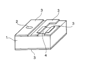
Fig. 1 is a diagram schematically illustrating a
metallized substrate according to an embodiment of the
.
CA 022~2113 1998-10-28
present invention. 1: substrate of aluminum nitride, 2:
via-hole, 3: thin metal film, and 4: thin resistance layer
are shown in Fig. 1.
DETAILED DESCRIPTION OF THE INVENTION
In the present invention, the substrate obtained by
filling through holes in the sintered product of aluminum
nitride with an electrically conducting layer, stands for
a sintered product of aluminum nitride having so-called
via-holes. Though there is no particular limitation, the
10 through hole has a diameter of from 0.03 to 0.50 mm, and a
ratio (length/diameter) of the diameter of the through
hole to the length thereof is not larger than 40.
Furthermore, there is no particular limitation on the
material constituting the electrically conducting layer
provided it is a refractory metal. Usually, however, this
material is such a refractory metal as tungsten or
molybdenum. In particular, it is desired that the
aluminum nitride is contained in an amount of from 2 to 10
parts by weight per 100 parts by weight of the refractory
metal. There is no particular limitation on the ratio of
the volume of the whole sintered product of aluminum
nitride including via-holes to the whole volume of the
via-holes which form the electrically conducting layer.
However, this ratio is usually from 0.1 to 20%.
The substrate comprising a sintered product of
aluminum nitride including via-holes of the present
invention has a feature in that the sintered product of
aluminum nitride has a therma1 conductivity of not smaller
than 190 W/mK and that the adhesion strength between the
sintered product of aluminum nitride and the electrically
conducting layer is not smaller than 5.0 kg/mm2.
The aluminum nitride substrate of the present
invention is a so-called composite system including via-
holes of a refractory metal. Therefore, it is difficult
to correctly evaluate the thermal conductivity of the
CA 022~2113 1998-10-28
aluminum nitride substrate itself. According to the
present invention, therefore, the thermal conductivity of
the aluminum nitride substrate made of the same starting
materials through the same dewaxing/firing batch without
via-hole, is employed as the thermal conductivity of the
sintered product of aluminum nitride. In the present
invention, the thermal conductivity is measured at 25 C.
According to the present invention, the adhesion
strength between the sintered product of aluminum nitride
and the electrically conducting layer stands for a
breaking strength measured by cutting the substrate across
the center of the via-hole, polishing the cut surface like
a mirror surface, forming a thin Ti/Pt/Au film on the cut
surface, soldering a pin of a diameter of 0.5 mm having a
flat end in a manner to come in contact with the surface
of the via-hole perpendicularly thereto, and pulling the
pin from a direction perpendicular thereto.
So far, it was difficult to accomplish both a high
thermal conductivity of the sintered product of aluminum
nitride and a large adhesion strength between the sintered
product of aluminum nitride and the electrically
conducting layer. However, the substrate of the present
invention is an excellent one exhibiting the thermal
conductivity of the sintered product of aluminum nitride
of not smaller than 190 W/mK and an a & esion strength
between the sintered product of aluminum nitride and the
conducting layer of not smaller than 5.0 kg/mm2, thus
exhibiting both a high thermal conductivity and a large
a & esion strength to the electrically conducting layer.
If the production conditions are selected from more
preferable ranges, it is allowed to obtain a substrate in
which the thermal conductivity of the sintered product of
aluminum nitride is not smaller than 200 W/mk and the
adhesion strength between the sintered product of aluminum
nitride and the electrically conducting layer is not
CA 022j2113 1998-10-28
..
smaller than 7.0 kg/mm2 and, preferably, not smaller than
10 . O kg/mm2 .
In the present invention, there is no particular
limitation on the electrically conducting patterns formed
on both surfaces of the substrate provided they have an
electrically conducting property. Usually, however, a
thin metal film, a thick-film formed out of a mixture of a
metal powder and an inorganic binder such as glass or the
like, or a mixture of a metal powder and an organic
binder, is used to form the electrically conducting
patterns. Among them, a thin metal film is most
preferably used because of its high electrically
conducting property. Known metals can be used without any
particular limitation for a thin metal film. Among them,
titanium (Ti), chromium (Cr), molybdenum (Mo), tungsten
(W), aluminum (Al), tantalum (Ta), tungsten-titanium (W-
Ti), nickel-chromium (Ni-Cr) and tantalum nitride (Ta-N)
can be favorably used since they can be intimately adhered
to the aluminum nitride substrate.
These metals may be used in a single kind or in a
combination of two or more kinds. The electrically
conducting patterns may be of a single layer or may be a
laminate of two or more layers.
When used being laminated in two or more layers, the
above-mentioned metals can be favorably adhered to the
aluminum nitride substrate and can, hence, be favorably
used as the first layer that comes in direct contact with
the aluminum nitride substrate. Among them, titanium
exhibits large and stable adhesion strength, and is more
preferably used. There is no particular limitation on the
thickness of the first layer when the first layer is used
as the adhesion layer. Usually, however, the first layer
has a thickness of from 0.01 ~m to 10 ~m and, more
preferably, from 0.05 ~m to 5 ~m from the standpoint of
reliably maintaining the adhesion strength resulting from
CA 022~2113 1998-10-28
an increased film thickness, reducing the time for forming
the film having a decreased thickness, and economical
advantage resulting from decreased amounts of starting
materials.
Here, the adhesion strength between the sintered
product of aluminum nitride and the electrically
conducting pattern stands for a breaking strength measured
by soldering a pin of a diameter of 0.5 mm having a flat
end to the uppermost layer of the electrically conducting
pattern perpendicularly thereto, and pulling the pin from
a direction perpendicularly t;hereto.
A known metal can be used as the second layer
laminated on the first layer. When the laminated
electrically conducting patterns of two layers are formed
and when the second layer is the uppermost layer, there
can be used at least any one of platinum (Pt), nickel
(Ni), palladium (Pd), copper (Cu), silver (Ag), or gold
(Au) because of their favorable electrically conducting
property. Among them, Pt, Pd, Ag and Au are more
favorably used because of their good resistance against
the corrosion. As will be described later, furthermore,
when the electrically conducting patterns have three or
more layers by laminating other films on the second layer,
there is favorably used Pt, Ni, Pd, W, W-Ti or Mo having a
high diffusion-preventing ability in order to prevent the
diffusion of elements between the first layer and the
third layer and to stably maintain the adhesion strength
between the electrically conducting patterns and the
substrate. There is no particular limitation on the
thickness of the second layer. On account of the same
reasons as the first layer, however, the second layer
usually has a thickness of from 0.05 to 10 ~m and,
preferably, from 0.1 to 5 ~m.
When a third layer is to be laminated on the second
layer, furthermore, a known metal can be used as the third
CA 022~2113 1998-10-28
layer. For example, at least any one of Pt, Ni, Pd, Cu,
Ag and Au can be favorably used because of their good
electrically conducting property. Among them, Pt, Pd, Ag
or Au is more favorably used because of their excellent
resistance against the corrosion. There is no particular
limitation on the thickness of the third layer. Usually,
however, the third layer has a thickness of from 0.05 ~m
to 10 ~m from the standpoint of stable and reliable
properties such as electric conductivity and economy.
In order to facilitate the soldering of semiconductor
elements on the uppermost metal layer, furthermore, at
least one kind of solder layer may be laminated and
patterned thereon, such as gold-tin (Au-Sn) solder, lead-
tin (Pb-Sn) solder, gold-silicon (Au-Si) solder or gold-
germanium (Au-Ge) solder. Mcreover, a layer for
preventing the diffusion of the soldering material may be
provided between the uppermost metal layer and the solder
layer. As the diffusion-preventing layer, Pt, Ni, Pd, W,
W-Ti or Mo is preferably used to exhibit a high diffusion-
preventing ability.
In order to maintain a predetermined electricresistance between the particular patterns in the above-
mentioned electrically conducting patterns, furthermore, a
thin resistance film pattern may be formed between the
particular patterns of the electrically conducting
patterns so as to be connected thereto maintaining the
predetermined resistance. It is desired that the
resistance of the thin resistance film pattern changes
little with the passage of time. It is further desired
that the resistance does not change irrespective of a
change in the temperature of the metallized substrate.
Though there is no particular limitation on the kind
of the thin resistance film used for the pattern, usually,
there is preferably used Ta-N or Ni-Cr from the standpoint
of stably maintaining the resistance. The composition of
-
CA 022~2113 1998-10-28
the alloy may preferably be so selected that the
resistance changes little with the change in the
temperature. In the case of, for example, Ta-N, a
composition including a Ta2N phase is preferably used.
Despite the pattern size is the same, furthermore, the
resistance increases with a decrease in the thickness of
the thin resistance film pattern, and the resistance
decreases with an increase in the thickness of the thin
resistance film pattern. Accordingly, the thickness is
suitably selected depending upon the required size of the
pattern and the resistance. Usually, however, the
thickness is selected to be from 0.01 ~m to 0.5 ~m from
the standpoint of stability in the resistance and economy.
Next, described below is a process for producing the
aluminum nitride substrate and the metallized substrate of
the present invention.
In the present invention, there is no particular
limitation on the aluminum nitride powder constituting the
molded article of aluminum nitride, and a known one can be
used. There can be preferably used a powder having an
average particle diameter of not larger than 5 ~m, and
there can be more preferably used a powder having an
average particle diameter of not larger than 3 ~m, and
there can be most preferably used a powder having an
average particle diameter of from 0.5 to 2 ~m as measured
by the sedimentation method. Moreover, the aluminum
nitride powder having an average particle diameter D1 as
calculated from the specific surface area thereof and an
average particle diameter D2 as measured by the
sedimentation method, satisfying the following formulas,
0.2 ~M ~ D1 < 1.5 ~m
D2/D1 < 2.60
exhibits a decreased coefficient of linear contraction
during the firing, contributes to improving the
dimensional stability of the sintered product and,
~, . ,
CA 022~2113 1998-10-28
besides, exhibits a coefficient of linear contraction
close to that of the electrically conducting paste layer,
making it possible to further increase the adhesion
strength between the sintered product of aluminum nitride
and the electrically conducting layer.
It is desired that the aluminum nitride powder
contains oxygen in an amount of not larger than 3.0% by
weight, and, when the aluminum nitride composition is AlN,
contains cationic impurities in an amount of not larger
than 0.5% by weight, and, particularly, contains oxygen in
an amount of from 0.4 to 1.0~ by weight, contains cationic
impurities in an amount of nc,t larger than 0.2% by weight,
the total amount of Fe, Ca, Si and C in the cationic
impurities being not larger than 0.17% by weight. The
above aluminum nitride powder is preferably used in the
present invention since it helps increase the thermal
conductivity of the obtained sintered product of aluminum
nitride.
A known sintering assistant can be used in the
present invention without any particular limitation.
Concretely speaking, there can be used an alkaline earth
metal compound such as oxides like calcium oxide, a
compound of yttrium or a lanthanide element such as oxides
like yttrium oxide.
Moreover, a known organic binder can be used in the
present invention without any particular limitation.
Concretely speaking, there can be used an acrylic resin
such as polyacrylic ester or polymethacrylic ester; a
cellulose resin such as methyl cellulose, hydroxymethyl
cellulose, nitrocellulose or cellulose acetate butylate; a
vinyl group-containing resin such as polyvinyl butyral,
polyvinyl alcohol or polyvinyl chloride; a hydrocarbon
resin such as polyolefin; or an oxygen-containing resin
such as polyethylene oxide, in one kind or being mixed in
two or more kinds. Among them, the acrylic resin can be
CA 022~2113 1998-10-28
favorably used since it is favorably dewaxed and enables
the resistance of the via-hole to be lowered.
Furthermore, known solvents, dispersants, plasticizers and
other components can be used without any particular
limitation.
In the present invention, the above-mentioned
components constituting the molded article of aluminum
nitride are blended at known ratios without any particular
limitation. For example, the sintering assistant is used
in an amount of from 0.01 to 10 parts by weight and the
organic binder is used in an amount of from 0.1 to 30
parts by weight per 100 parts by weight of the aluminum
nitride. In particular, the aluminum nitride containing 2
to 7 parts by weight of the sintering assistant is
advantageous for increasing the thermal conductivity and
is, hence, preferably used. There is no particular
limitation on the method of preparing a molded article of
aluminum nitride using the above-mentioned components.
Generally, however, the aluminum nitride is molded as a
green sheet by the doctor blade method. The green sheet
may be used as a single layer or may be used as a laminate
of a plurality of sheets.
In the present invention, there is no particular
limitation on the refractory metal powder constituting the
electrically conducting paste provided it has a melting
point higher than the sintering temperature of the
aluminum nitride. Concretely speaking, there can be used
such a metal as tungsten or molybdenum. The refractory
metal powder that is generally preferably used has an
average particle diameter of from 1 to 2.5 ~m and, most
preferably, from 1.6 to 2.0 ~m as measured by the
Fischer's method, since it is effective in preventing the
occurrence of cracks in the via-holes.
Moreover, a known aluminum nitride powder is used for
the electrically conducting paste without any particular
CA 022~2ll3 l998-l0-28
13
limitation. In particular, the aluminum nitride powder
that is suitably used for the molded article of aluminum
nitride is sintered well with the powder of the refractory
metal, and is effective in improving the adhesion of the
electrically conducting layer, helps decrease the
difference in the coefficient of contraction between the
aluminum nitride and the electrically conducting layer,
and further helps improve the ~;men~ional stability of the
sintered product.
In the present invention, the electrically conducting
paste has a composition in which 100 parts by weight of
the refractory metal powder is blended with 2 to 10 parts
by weight of the aluminum nitride powder. In the
composition of the electrically conducting paste, when the
ratio of the aluminum nitride powder is smaller than 2
parts by weight, the adhesion strength decreases between
the electrically conducting layer and the sintered product
of aluminum nitride, or the difference in the coefficient
of contraction increases between the substrate of aluminum
nitride and the electrically conducting layer, resulting
in the development of a gap in the junction interface.
When the ratio of the aluminum nitride is greater than 10
parts by weight, on the other hand, the viscosity of the
electrically conducting paste so increases that it is
poorly introduced, and voids that consequently develop
decrease the adhesion strengt.h between the electrically
conducting layer and the sintered product of aluminum
nitride. Or, the surface of the electrically conducting
layer tends to be discolored due to the aluminum nitride,
and the resistance increases. When the blended amount of
the aluminum nitride powder is from 3 to 7 parts by
weight, the difference in the coefficient of contraction
due to the firing is very small between the via-hole and
the ceramics. Therefore, only small stress is produced
around the via-holes, and the electric resistance of the
CA 022~2ll3 l998-l0-28
14
via-holes r~m~; n.s small. In order to obtain a paste-like
composition of the refractory metal powder and the
aluminum nitride powder, in general, this composition is
usually mixed with an acrylic resin such as polyacrylic
ester or polymethacrylic esteri a cellulose resin such as
methyl cellulose, ethyl cellulose, hydroxymethyl
cellulose, nitrocellulose, or cellulose acetate butylate;
a vinyl group-cont~;n;ng resin such as polyvinyl butyral,
polyvinyl alcohol or polyvinyl chloride; a hydrocarbon
resin such as polyolefin; an organic binder such as
polyethylene oxide; or an organic solvent such as di-n-
butyl phthalate, diethylene glycol mono-n-hexyl ether, 2-
(2-butoxyethoxy)ethyl acetate or terpineol, to maintain a
suitable viscosity which is, generally, from 100 to 30000
poises at 25 C/5 rpm. In preparing the electrically
conducting paste, any other known dispersant, plasticizer
or component may be used without any limitation.
In the present invention, the through holes in the
molded article of aluminum nitride are filled with the
electrically conducting paste to obtain a molded article
having via-holes. There is no particular limitation on
the method of forming through holes in the molded article
of aluminum nitride, and a generally employed method is
used such as metal mold punching method or a method using
a punching machine. There is no particular limitation on
the size of the through hole. However, the through hole
having a diameter of from 0.05 to 0.50 mm permits the
electrically conducting paste to be easily filled therein,
maintains a balance in the coefficient of contraction
between the aluminum nitride and the electrically
conducting layer, and is preferably employed.
A known method can be used without any particular
limitation for filling the through holes formed in the
molded article of aluminum nitride with the above-
mentioned electrically conducting paste. Concretely
. .
CA 022~2113 1998-10-28
speaking, a printing method or a pressurized introduction
method can be used. When the through hole has a ratio
(length/diameter) of the diameter to the length thereof
that is greater than 2.5, the pressurized introduction
method is preferred since it makes it possible to fill the
electrically conducting paste more efficiently.
In the present invention, the molded article of
aluminum nitride having the above-mentioned via-holes may
be dewaxed so that the content of residual carbon in the
molded article of aluminum nitride is from 800 to 3000 ppm
and, preferably, from 1200 to 2500 ppm. When the content
of residual carbon is smaller than 800 ppm, the thermal
conductivity of the sintered product of aluminum nitride
becomes smaller than 190 W/mK, and the object of the
present invention is not accomplished. When the content
of residual carbon exceeds 3000 ppm, on the other hand,
the refractory metal powder is poorly sintered, making it
difficult to obtain a uniform and sufficiently large
adhesion strength between the sintered product of aluminum ,
nitride and the electrically conducting layer. Besides,
cracks develop in the aluminum nitride and the substrate
of the sintered product of aluminum nitride is warped to a
large extent, making it difficult to accomplish the object
of the present invention.
There is no particular limitation on the method of
dewaxing the molded article of aluminum nitride so that
the content of residual carbon therein lies within a range
of from 800 to 3000 ppm. There is no particular
limitation on the atmosphere for dewaxing provided the
oxidizing atmosphere such as the open air is excluded that
may oxidize the refractory metal. Concretely speaking,
there can be preferably employed an inert gaseous
atmosphere such as of nitrogen, argon or helium; a
reducing gaseous atmosphere such as of hydrogen; a mixed
gaseous atmosphere thereof: a wet gaseous atmosphere
.
CA 022~2ll3 l998-l0-28
16
thereof; or vacuum.
The dewaxing temperature can be suitably selected.
Usually, however, the dewaxing temperature is from 500 to
1200 C and, preferably, from 800 to 1000-C. There is no
particular limitation on the rate of elevating the
temperature to the above-mentioned value. Preferably,
however, the rate of elevating the temperature is not
larger than 10 C/min.
Moreover, the dewaxing time may be so set that the
content of residual carbon in the molded article after
dewaxed is from 800 to 3000 ppm. The dewaxing time cannot
be exclusively specified since it varies to some extent
depending upon such a condition as the thickness of the
molded article, density of the molded article, ratio
occupied by the via-holes and the dewaxing temperature.
Generally, however, the dewaxing time is from 1 to 600
minutes.
In the present invention, the molded article of
aluminum nitride (hereinafter referred to as "dewaxed
materialN) having via-holes and having a content of
residual carbon of 800 to 3000 ppm therein, is then fired
in a nonoxidizing atmosphere or in a dry reducing gaseous
atmosphere. As the nonoxidizing atmosphere, use is made
of a single gas such as nitrogen, argon or helium, or a
mixture thereof. Or, the firing is conducted in vacuum or
in a reduced-pressure atmosphere. As the dry reducing
gaseous atmosphere, use is made of hydrogen or a gaseous
atmosphere of a mixture of hydrogen and an inert gas. It
is important that the firing is conducted at a temperature
of from 1200 to 1700 C and, preferably, from 1500 to
1650 C in a first step and, then, at a temperature of from
1800 to 1950-C and, preferably, from 1820 to 1900-C in a
second step. That is, when the firing temperature in the
first step is lower than 1200 C, the reaction for removing
oxygen in the aluminum nitride by reduction with carbon
CA 022~2113 1998-10-28
r~m~;n'ng in the dewaxed product proceeds little, the
thermal conductivity of the sintered product of aluminum
nitride becomes smaller than 190 W/mK, and the object of
the present invention is not accomplished. When the
firing temperature in the first step exceeds 1700-C, on
the other hand, the aluminum nitride is sintered before
the reaction for removing oxygen in the aluminum nitride
by reduction with residual carbon proceeds to a
satisfactory degree. Consequently, oxygen diffuses and
dissolves in the aluminum nitride as a solid solution, the
sintered product of aluminum nitride fails to exhibit a
high thermal conductivity, and the object of the present
invention is not accomplished. When the firing
temperature in the first step is from 1500 to 1650-C, the
reaction for removing oxygen by reduction proceeds
efficiently, which is desirable. When the firing
temperature in the second step is lower than 1800-C, the
aluminum nitride is not sintered to a sufficient degree,
the thermal conductivity of the sintered product of
aluminum nitride becomes lower than 190 W/mK, and the
object of the present invention is not accomplished. When
the firing temperature of the second step exceeds 1950-C,
the adhesion strength between the electrically conducting
layer forming via-holes and the substrate decreases and,
besides, the sintered product is warped to a degree
greater than 200 ~m, making it difficult to accomplish the
object of the present invention. Though there is no
particular limitation, the temperature is elevated to such
a value generally at a rate of 1 to 40 C/min. Though
there is no particular limitation, it is desired that the
above-mentioned temperatures are maintained for a period
of time of from 30 minutes to 10 hours in the first step
and from 1 minute to 20 hours in the second step. The
firing may be executed in one time without dropping the
firing temperatures in the first and second steps during
. . .
CA 022~2ll3 l998-l0-28
18
the process, or may be executed being divided into two
times by dropping the firing temperature between the first
step and the second step. From the standpoint of time and
energy efficiency, however, it is desired that the firing
is executed in one time without dropping the temperature
during the process.
The aluminum nitride substrate having via-holes of
the present invention is used usually being metallized
with a thin film on the surfaces thereof. For example,
electrically conducting patterns are formed on the
opposing two surfaces of the aluminum nitride substrate
having via-holes obtained through the above-mentioned
method, and at least portions of the electrically
conducting patterns are electrically connected together
through the via-holes thereby to obtain a metallized
substrate of the present invention.
When the electrically conducting patterns are to be
formed on the surfaces of the substrate, it is desired to
grind or polish the surfaces of the substrate in order to
increase the adhesion strength between the electrically
conducting patterns and the substrate. The grinding and
polishing can be effected relying upon a known technology
without any limitation, which, usually, may be lapping,
polishing, barrel-polishing, sand-blasting or polishing
using a grinder. The surface coarseness of the substrate
may differ depending upon the object. Usually, however,
the center line average coarseness (Ra) of not larger than
0.8 ~m and, more preferably, not larger than 0.05 ~m is
desirable from the standpoint of highly reliably soldering
the semiconductor elements, etc.
The electrically conducting patterns can be formed by
a known technology without any limitation. The thin metal
films constituting the electrically conducting patterns
can be formed relying on a known technology such as
sputtering method, vaporization method, chemical vapor-
,,
CA 022~2113 1998-10-28
phase deposition method (CVD), ion-plating method, melt-
injection method, screen-printing method or sol/gel
coating method based on a spin coating or dipping method.
When the thin metal films constituting the electrically
conducting patterns are to be formed by, for example,
sputtering method, a target cont~;n;ng components of the
thin metal films is used, the temperature of the substrate
is usually set to be from room temperature to 300 C, the
interior of the vacuum vessel is evacuated to be not
higher than 2 x 10⁻³ Pa, argon gas is introduced at a rate
of 10 to 80 cc/min, the pressure in the vacuum vessel is
maintained at 0.2 to 1.0 Pa, and the power of the RF
(high-frequency) power source is set to be from 0.2 to 3
kW in order to form the thin metal films maint~;n;ng a
predetermined thickness.
When a thin film of a nitride such as Ta-N or a thin
film of an oxide is to be formed for constituting a thin
resistance film pattern, the reactive sputtering method is
preferably employed. According to the reactive sputtering
method, a target containing metal components of a compound
is used, and the reaction gas containing other components
of the compound such as nitrogen or oxygen is introduced
into the vacuum vessel simultaneously with a discharge
gas, in order to obtain a thin film. The composition of
the obtained thin film is determined depending upon a
ratio of introducing the discharge gas and the reaction
gas.
The Ta-N film is formed by the reactive sputtering
by, for example, using Ta as a target, usually setting the
temperature of the substrate to be room temperature to
300 C, evacuating the interior of the vacuum vessel to be
not higher than 2 x 10⁻³ Pa, introducing argon which is a
discharge gas at a rate of lt) to 80 cc/min., introducing
nitrogen which is a reaction gas at a rate of 0.3 to 0.7
times as much as the rate of introducing the argon gas,
_
CA 022~2113 1998-10-28
maintaining the pressure in the vacuum vessel at 0.2 to
1.O Pa, and setting the power of the RF (high-fre~uency)
power source at 0.2 to 3 kW to form the Ta-N film
maint~; n; ng a predetermined thickness.
According to the present invention, any electrically
conducting pattern can be formed depending upon the use by
patterning the thin metal film from which the electrically
conducting patterns are to be constituted. The patterning
can be effected by any known technology depending upon the
use of the substrate. Concretely speaking, a metal-
masking method, a wet-etching method, a lift-off method or
a dry-etching method can be employed. When the thin metal
films are to be patterned by, for example, the metal-
masking method, a metal mask forming a predetermined
pattern is secured onto the aluminum nitride substrate
having an electrically conducting layer formed in the
through hole, and the electrically conducting patterns are
formed by the sputtering method or the vapor deposition
method. When the electrically conducting patterns are to
be formed by the dry-etching method, furthermore, the thin
metal film constituting the electrically conducting
pattern is formed by the sputtering method or the
vaporization method on the aluminum nitride substrate, a
predetermined pattern is formed with photo-resist and so
on the thin metal film, unnecessary portion of the thin
metal film is removed by ion milling or the like method,
and the resist is peeled off, thereby to accomplish the
patterning.
There is no particular limitation on the method of
forming electrically conducting patterns of when a thin
resistance film pattern is included in the wiring pattern.
However, the electrically conducting pattern is formed by
the following methods. According to one method, the
electrically conducting pattern which is added connection
portions to the thin reistance film pattern is, first,
CA 022S2113 1998-10-28
formed on the aluminum nitride substrate. Next, the thin
resistance film constituting the thin resistance film
pattern is laminated on the electrically conducting
pattern thereby to form the thin resistance film pattern.
According to this method, there can be obtained a wiring
pattern of a shape in which the thin resistance film is
laminated on the electrically conducting pattern in the
connection portions. According to another method, the
thin resistance film pattern of a shape including the
connection portions is formed in advance on the aluminum
nitride substrate, and a thin metal film constituting a
electrically conducting is laminated on the thin
resistance film pattern to form an electrically conducting
pattern. This method makes it possible to obtain a wiring
pattern of the shape in which the electrically conducting
is laminated on the thin resistance film in the connection
portions. According to a further method, the thin
resistance film is used as a first layer that is in direct
contact with the aluminum nitride substrate, a thin metal
film having an electric resistivity smaller than that of
the thin resistance film is laminated thereon to form an
electrically conducting pattern, and the thin metal film
on the thin resistance film is partly removed from only a
portion between particular patterns where a predetermined
resistance is re~uired, in order to form an electrically
conducting pattern including the thin resistance film
pattern in the pattern.
In order to suppress the change in the resistance due
to the lapse of time and temperature, the thus obtained
thin resistance pattern is usually coated on its surface
with an oxide film in order lo stabilize the resistance
(treatment for stabilizing the resistance). A known
technology can be used without any limitation to stabilize
the resistance. Concretely speaking, the resistance is
stabilized by forming an oxide film based on the anodic
CA 022j2113 1998-10-28
oxidation method or by forming an oxide film by heating
the substrate on which the thin resistance film pattern is
formed in the open air. Furthermore, the resistance of
the thus formed thin resistance film pattern can be
adjusted by a known technology without any limitation.
Concretely speaking, the resistance is adjusted by the
laser trimming method or by heating the substrate on which
the thin resistance film pattern is formed in the open
air.
As will be comprehended from the foregoing
description, the substrate of the present invention has a
thermal conductivity of not smaller than 190 W/mK at 25'C,
exhibits an adhesion strength of as sufficiently large as
5.0 kg/mm2 or greater between the sintered product of
aluminum nitride and the electrically conducting layer
forming via-holes, does not develop cracks in the sintered
product of aluminum nitride or in the via-holes, and is
warped little. Besides, the metallized substrate has
electrically conducting patterns formed on the opposing
surfaces thereof, and at least portions of the
electrically conducting patterns on both surfaces thereof
are electrically connected together through the via-holes,
exhibits an excellent adhesion strength between the thin
metal film constituting the electrically conducting
pattern and the via-hole. The substrate and the
metallized substrate of the present invention have
therefore offered a very great industrial value. The
aluminum nitride substrate that is metallized of the
present invention can be favorably used as a sub-mount or
a chip carrier for a laser diode and a light-emitting
diode, and as parts for elect:ronic and semiconductor
devices such as heat sink, IC' package, etc.
According to the process for producing substrates of
the present invention, furthermore, there is obtained a
substrate exhibiting a thermal conductivity of not smaller
CA 022~2113 1998-10-28
than 190 W/mK at 25 C and an adhesion strength of as
sufficiently large as 5.0 kg/mm2 or more between the
sintered product of aluminum nitride and the electrically
conducting layer forming via-holes, without developing
cracks or discoloration in the sintered product of
aluminum nitride or in the via-holes, warping little, and
offering a very great industrial value.
EXAMPLES
The invention will now be concretely described by way
of examples to which only, however, the invention is in no
way limited.
In Examples and Comparative Examples, the contents of
residual carbon were analyzed by using a nondiffusion-type
infrared ray-absorptive carbon analyzer (EMIA-110,
manufactured by Horiba Seisakusho Co.).
The average particle diameter D1 based on the
specific surface area was calculated in accordance with
the following formula,
D1 (~m) = 6/(S x 3.26)
[S: specific surface area of an AlN powder (m2/g)]
The average particle diameter D2 based on the
sedimentation method was measured by using a centrifugal
particle size distribution-measuring apparatus, CAPA5000,
manufactured by Horiba Seisakusho Co.
The appearance of the sintered product of aluminum
nitride was observed by naked eyes and by using a
stereomicroscope (x40). The warping of the sintered
product of aluminum nitride was measured by using a
micrometer equipped with a surface plate manufactured by
Mitsutoyo Co.
The adhesion strength between the sintered product of
aluminum nitride and the electrically conducting layer was
measured as described below. First, the substrate was cut
across the center of the via-hole of the sintered product
of aluminum nitride having through holes filled with the
CA 022~2113 1998-10-28
24
electrically conducting layer. The cut surface was
polished like a mirror surface, a thin film of Ti/Pt/Au
was formed on the cut surface, and a pin plated with Ni
was soldered to the surface of the via-hole
perpendicularly thereto so as to come in contact
therewith. The pin was made of a 42 -alloy having a flat
end and a diameter of 0.5 mm. The solder was composed of
60% by weight of tin and 4096 by weight of lead. The pin
was set to a Strograph, M2, manufactured by Toyo Seiki
Co., and was pulled from a perpendicular direction to
measure the breaking strength. The pulling speed was 10
mm/min. The peeling mode was examined by observing the
broken surfaces of the pin and of the sintered product
after the testing by using the stereomicroscope (x40), a
metallized microscope (x400) and an X-ray microanalyzer.
The electrically conduct:ing patterns were formed on
the substrate of the sintered product of aluminum nitride
having through holes filled with the electrically
conducting layer. That is, by using a diamond grain, the
surfaces of the substrate were machined until the
thickness of the substrate was 0.22 mm and until mirror
surfaces were formed. The center line average coarseness
(Ra) on the surfaces of the thus obtained substrate was
measured by using a Surfcom, 550A, manufactured by Tokyo
Seimitsu Co. to be 0 .02 ,~Lm.
The machined substrate was washed with ultrasonic
waves in methylene chloride, dried in the vapor of
methylene chloride, and thin metal films 3 were formed by
sputtering on both the front and back surfaces thereof
(first layer/second layer/ third layer = Ti:0.1 ~m/Pt:0.2
~m/Au:0.5 ~m). During the sputtering, the substrate was
heated at 150 C, the interior of the vacuum vessel was
evacuated to be not higher than 2 x
10-3 Pa, an argon gas was introduced to maintain the
pressure of 0.6 Pa in the vacuum vessel, and the films
CA 022~2113 1998-10-28
were formed by using targets of Ti, Pt and Au successively
under a condition of RF 0.5 }cW. After the thin metal
films 3 were formed, the thin metal film 3 on the front
side was etched by dry-etching to form the electrically
conducting pattern.
Then, a Ta-N layer for constituting a thin resistance
film was formed by the reactive sputtering method
maint~;n;ng a thickness of 0.1 ~m on the whole front
surface inclusive of the thin metal film 3. In the
reactive sputtering method, the substrate was heated at
150 C, the interior of the vacuum vessel was evacuated to
be not higher than 2 x 10⁻³ Pa, an argon gas and an N2 gas
were introduced to maintain a pressure of 0.6 Pa in the
vacuum vessel, and the film was formed using a Ta target
under a condition of RF 0.5 kW. The argon gas and the N2
gas were introduced at a ratio of 1:0.6. The Ta-N layer
was analyzed by using a fully automatic X-ray analyzer
manufactured by Nippon Phillips Co. to observe a
diffraction peak due to a Ta2N phase. After the Ta-N
layer has been laminated, the Ta-N layer of undesired
portions was removed by wet-etching, thereby to form a
thin resistance layer 4. After the thin resistance layer
was formed, the substrate was heated at 360 C for 4 hours
in the open air to stabilize the resistance.
After the stabilization treatment, the metallized
substrate was cut by a dicing machine into pieces each
having a length of 1.0 mm and a width of 1.0 mm to thereby
prepare a metallized substrate that is shown in Fig. 1.
The adhesion strength between the electrically
conducting pattern on the metallized substrate and the
via-hole was measured according to a method described
below. That is, by using a substrate on which the thin
metal film has been formed but the pattern has not yet
been formed, a nickel-plated pin having a diameter of 0.5
mm was soldered onto the thin metal film on the via-hole
CA 022~2113 1998-10-28
in the substrate perpendicularly thereto so that the whole
thin metal film on the via-hcle was covered by the pin.
The solder used was the same as the one used for measuring
the adhesion strength described above. Then, the pin was
pulled to find the breaking strength according to the same
method as the one for measuring the strength described
above, and the breaking strength was regarded to be the
adhesion strength between the thin metal film that was
formed and the via-hole.
The electric resistance of the via-hole in the
metallized substrate cut by the dicing machine and the
electric resistance of the thin resistance layer 4, were
measured according to the following method. That is, as
for the electric resistance of the via-hole, the back
surface of the metallized substrate was soldered onto the
metal substrate by using the same solder as the one used
for measuring the adhesion strength, a needle-like
measuring probe was brought into contact with the
electrically conducting pattern on the via-hole on the
front surface, and the electric resistance was measured
between the probe and the metal substrate that was
soldered. As for the electric resistance of the thin
resistance layer 4, the two measuring probes were brought
into contact with the each two electrically conducting
patterns connected to both sides of the thin resistance
layer 4, and the electric resistance was measured relying
on the four-terminal method.
(Example 1)
100 Parts by weight of an aluminum nitride powder
having an average particle diameter of 1.50 ~m as measured
by the sedimentation method, a specific surface area of
2.50 m2/g and, hence, an average particle diameter of 0.74
~m as calculated from the specific surface area, an oxygen
content of 0.80% and having a composition shown in Table
1, as well as 5 parts by weight of yttria, 2 parts by
CA 022~2113 1998-10-28
weight of an n-butyl methacrylate as a dispersant, 11
parts by weight of a polybutyl acrylate as an organic
binder, 7 parts by weight of a dioctyl phthalate as a
plasticizer, and 50 parts by weight of a toluene-isopropyl
alcohol mixture solvent, were weighed, thrown into a ball
mill pot, and were mixed together to a sufficient degree
by using nylon balls. The obtained slurry was introduced
into a defoaming machine so as to have a viscosity of
20000 cps, and was molded into a sheet on a polypropylene
film by using a sheet-molding machine of the doctor blade-
type to prepare a green sheet of aluminum nitride having a
thickness of about 0.50 mm. The green sheet was cut into
a size of 65 x 65 mm. Three pieces of the green sheets of
aluminum nitride were laminated one upon the other. The
pressure for lamination was 50 kgf/cm2, the temperature
for lamination was 80 C, and the time for lamination was
15 minutes. The laminated green sheet measuring 65 x 65
mm was punched by using a punching metal mold having a
diameter of 0.65 mm maintaining a pitch of 1.5 mm in order
to form through holes arranged in a number of 40 x 40.
Next, 5 parts by weight of the aluminum nitride powder,
1.5 parts by weight of an ethyl cellulose as an organic
binder, 5.0 parts by weight of a 2-(2-butoxyethoxy)ethyl
acetate as a solvent, and other plasticizers and
dispersants were sufficiently kneaded by using an
automatic mortar and then a roll mill having three rolls
together with 100 parts by weight of a tungsten powder
having an average particle diameter of 1.8 ~m as measured
by the Fischer's method to prepare a paste. The through
holes formed in the green sheet of aluminum nitride were
filled with the tungsten paste by the pressurized
introduction method. The filling pressure was 80 psi and
the filling time was 100 seconds.
The thus obtained molded article of aluminum nitride
having via-holes was heated and dewaxed at 900 C for 2
. . ,
CA 022~2ll3 l998-l0-28
28
hours while flowing a dry nitrogen gas at a rate of 30
liters a minute. The temperature was elevated at a rate
of 2. 5- C/min. At the same time, the heated and dewaxed
test sample was examined for its content of residual
carbon to be 1800 ppm. The dewaxed product was introduced
into a container made of aluminum nitride, heated at
1580-C in a nitrogen atmosphere for 6 hours (firing in the
first step) and was further heated at 1870-C for 10 hours
(firing in the second step). Cracks developed neither in
the sintered product of aluminum nitride forming the
substrate nor in the electrically conducting layer, and
the sintered product exhibited good appearance. The
substrate of the sintered product of aluminum nitride
warped by 45 ~Im as a whole. The adhesion strength of the
electrically conducting layer filled in the through hole
was measured to be 17.4 kg/mm2. The peeling mode was the
breakage in the solder in all cases.
The electrically conducting pattern and the thin
resistance layer were formed on the substrate which was
then cut by using a dicing machine. The electric
resistance in the via-hole in the metallized substrate was
measured to be 1. 5 mQ. The electric resistance of the
thin resistance layer was 20.1 Q. The adhesion strength
between the thin metal film 3 and the via-hole was 7.5
kg/mm2. The simultaneously dewaxed and fired test sample
(substrate) having a thickness of 0. 635 mm was measured
for its thermal conductivity to be 215 W/mk in compliance
with a laser flash method.
(Examples 2 to 6 and Comparative Examples 1 and 2)
The process was repeated in the same manner as in
Example 1 but changing the amount of addition of the
aluminum nitride powder to the electrically conducting
paste as shown in Table 2. The results were as shown in
Table 2. In Comparative Example 2, the electric
resistance of the thin resistance layer was measured.
CA 022~2113 1998-10-28
29
However, the thin resistance layer had been cut in the
pattern due to cracks in the sintered product, and there
was no electric conduction.
(Example 7)
The molded article of aluminum nitride having via-
holes prepared in Example 1 was heated and dewaxed at
900 C for 2 hours while flowing the dry nitrogen gas at a
rate of 18 liters a minute. The temperature was elevated
at a rate of 2.5 C/min. At the same time, the heated and
dewaxed test sample was examined for its content of
residual carbon to be 2800 ppm. The dewaxed product was
introduced into a container made of aluminum nitride,
heated at 1580 C in a nitrogen atmosphere for 6 hours
(firing in the first step) and was further heated at
1870 C for 10 hours (firing in the second step). Cracks
developed neither in the sintered product of aluminum
nitride forming the substrate nor in the electrically
conducting layer, and the sintered product exhibited good
appearance. The substrate of the sintered product of
aluminum nitride warped by 65 ~m as a whole. The adhesion
strength of the electrically conducting layer filled in
the through hole was measured to be 16.6 kg/mm2. The
peeling mode was the breakage in the solder in all cases.
The electrically conducting pattern and the thin
resistance layer were formed on the substrate which was
then cut by using a dicing machine. The electric
resistance in the via-hole in the metallized substrate was
measured to be 3.0 mQ. The electric resistance of the
thin resistance layer was 20.8 Q. The adhesion strength
between the thin metal film 3 and the via-hole was 7.6
kg/mm2. The simultaneously dewaxed and fired test sample
(substrate) having a thickness of 0.635 mm was measured
for its thermal conductivity to be 215 W/mk in compliance
with the laser flash method.
(Example 8)
~ .
CA 022~2ll3 l998-l0-28
The molded article of aluminum nitride having via-
holes prepared in Example 1 was heated and dewaxed at
900 C for 2 hours while flowing the dry nitrogen gas at a
rate of 23 liters a minute. The temperature was elevated
at a rate of 2.5 C/min. At the same time, the heated and
dewaxed test sample was examined for its content of
residual carbon to be 2500 ppm. The dewaxed product was
introduced into a container made of aluminum nitride,
heated at 1580~C in a nitrogen atmosphere for 6 hours
(firing in the first step) and was further heated at
1870-C for 10 hours (firing in the second step). Cracks
developed neither in the sintered product of aluminum
nitride forming the substrate nor in the electrically
conducting layer, and the sintered product exhibited good
15 appearance. The substrate of the sintered product of
aluminum nitride warped by 54 ~lm as a whole. The adhesion
strength of the electrically conducting layer filled in
the through hole was measured to be 16. 8 kg/mm2. The
peeling mode was the breakage in the solder in all cases.
The electrically conducting pattern and the thin
resistance layer were formed on the substrate which was
then cut by using a dicing machine. The electric
resistance in the via-hole in the metallized substrate was
measured to be 2.5 mQ. The electric resistance of the
25 thin resistance layer was 19. 8 n. The adhesion strength
between the thin metal film 3 and the via-hole was 7.1
kg/mm2. The simultaneously dewaxed and fired test sample
(substrate) having a thickness of 0. 635 mm was measured
for its thermal conductivity to be 215 W/mk in compliance
30 with the laser flash method.
(Example 9)
The molded article of aluminum nitride having via-
holes prepared in Example 1 was heated and dewaxed at
900 C for 2 hours while flowing the dry nitrogen gas at a
35 rate of 35 liters a minute. The temperature was elevated
CA 022~2113 1998-10-28
at a rate of 2.5 C/min. At the same time, the heated and
dewaxed test sample was examined for its content of
residual carbon to be 1200 ppm. The dewaxed product was
introduced into a container made of aluminum nitride,
heated at 1580 C in a nitrogen atmosphere for 6 hours
(firing in the first step) and was further heated at
1870 C for 10 hours (firing in the second step). Cracks
developed neither in the sintered product of aluminum
nitride forming the substrate nor in the electrically
conducting layer, and the sintered product exhibited good
appearance. The substrate of the sintered product of
aluminum nitride warped by 26 ~m as a whole. The adhesion
strength of the electrically conducting layer filled in
the through hole was measured to be 15.6 kg/mm2. The
peeling mode was the breakage in the solder in all cases.
The electrically conducting pattern and the thin
resistance layer were formed on the substrate which was
then cut by using a dicing machine. The electric
resistance in the via-hole in the metallized substrate was
measured to be 1.3 mQ. The electric resistance of the
thin resistance layer was 19.6 Q. The adhesion strength
between the thin metal film 3 and the via-hole was 8.9
kg/mm2. The simultaneously dewaxed and fired test sample
(substrate) having a thickness of 0.635 mm was measured
for its thermal conductivity to be 208 W/mk in compliance
with the laser flash method.
(Example 10)
The molded article of aluminum nitride having via-
holes prepared in Example 1 was heated and dewaxed at
900 C for 2 hours while flowing a mixture gas of dry
nitrogen and hydrogen at a rate of 30 liters a minute.
The temperature was elevated at a rate of 2.5 C/min. At
the same time, the heated and dewaxed test sample was
examined for its content of residual carbon to be 900 ppm.
The dewaxed product was introduced into a container made
CA 022~2113 1998-10-28
of aluminum nitride, heated at 1580 C in a nitrogen
atmosphere for 6 hours (firing in the first step) and was
further heated at 1870 C for 10 hours (firing in the
second step). Cracks developed neither in the sintered
product of aluminum nitride forming the substrate nor in
the electrically conducting layer, and the sintered
product exhibited good appearance. The substrate of the
sintered product of aluminum nitride warped by 18 ~m as a
whole. The adhesion strength of the electrically
conducting layer filled in the through hole was measured
to be 14.0 kg/mm2. The peeling mode was the breakage in
the solder in all cases.
The electrically conducting pattern and the thin
resistance layer were formed on the substrate which was
then cut by using a dicing machine. The electric
resistance in the via-hole in the metallized substrate was
measured to be 1.0 mQ. The electric resistance of the
thin resistance layer was 20.2 Q. The adhesion strength
between the thin metal film 3 and the via-hole was 7.2
kg/mm2. The simultaneously dewaxed and fired test sample
(substrate) having a thickness of 0.635 mm was measured
for its thermal conductivity to be 198 W/mk in compliance
with a laser flash method.
(Comparative Example 3)
The molded article of aluminum nitride having via-
holes prepared in Example 1 was heated and dewaxed at
900 C for 2 hours while flowing a mixture gas of dry
nitrogen and hydrogen at a rate of 20 liters a minute.
The temperature was elevated at a rate of 2.5 C/min. At
the same time, the heated and dewaxed test sample was
examined for its content of residual carbon to be 600 ppm.
The dewaxed product was introduced into a container made
of aluminum nitride, heated at 1580 C in a nitrogen
atmosphere for 6 hours (firing in the first step) and was
further heated at 1870 C for 10 hours (firing in the
.
CA 022~2113 1998-10-28
second step). Cracks developed neither in the sintered
product of aluminum nitride forming the substrate nor in
the electrically conducting layer, and the sintered
product exhibited good appearance. The substrate of the
sintered product of aluminum nitride warped by 15 ~m as a
whole. The adhesion strength of the electrically
conducting layer filled in the through hole was measured
to be 8.0 kg/mm2. The peeling occurred on the interface
between the tungsten layer and the sintered product of
aluminum nitride in all cases.
The electrically conducting pattern and the thin
resistance layer were formed on the substrate which was
then cut by using a dicing machine. The electric
resistance in the via-hole in the metallized substrate was
measured to be 0.9 mQ. The electric resistance of the
thin resistance layer was 20.8 n. The adhesion strength
between the thin metal film 3 and the via-hole was 6.0
kg/mm2. The simultaneously dewaxed and fired test sample
(substrate) having a thickness of 0.635 mm was measured
for its thermal conductivity to be 168 W/mk in compliance
with the laser flash method.
(Comparative Example 4)
The molded article of aluminum nitride having via-
holes prepared in Example 1 was heated and dewaxed at
900 C for 2 hours while flowing a dry nitrogen at a rate
of 5 liters a minute. The temperature was elevated at a
rate of 2.5 C/min. At the same time, the heated and
dewaxed test sample was examined for its content of
residual carbon to be 3500 ppm. The dewaxed product was
introduced into a container rnade of aluminurn nitride,
heated at 1580 C in a nitrogen atmosphere for 6 hours
(firing in the first step) and was further heated at
1870 C for 10 hours (firing in the second step). Cracks
developed in the sintered product of aluminum nitride
forming the substrate. The substrate of the sintered
. . ._ .
CA 022~2113 1998-10-28
34
product of aluminum nitride warped by 242 llm as a whole.
The adhesion strength of the electrically conducting layer
filled in the through hole was measured to be 3.3 kg/mm2.
The peeling occurred on the interface between the tungsten
layer and the sintered product of aluminum nitride in all
cases.
The electrically conducting pattern and the thin
resistance layer were formed on the substrate which was
then cut by using a dicing machine. The electric
resistance in the via-hole in the metallized substrate was
measured to be 8.9 mQ. Though the electric resistance of
the thin resistance layer was measured, the thin
resistance layer had been cut in the pattern due to cracks
in the sintered product, and there was no electric
conduction. The adhesion strength between the thin metal
film 3 and the via-hole was 2.8 kg/mm2. The
simultaneously dewaxed and fired test sample (substrate)
having a thickness of 0.635 mm was measured for its
thermal conductivity to be 195 W/mk in compliance with the
laser flash method.
(Examples 11 to 15 and Comparative Examples 5 and 6)
The process was carried out in the same manner as in
Example 1 but changing the firing temperature in the first
step as shown in Table 2. The results were as shown in
Table 2.
(Examples 16 to 18 and Comparative Examples 7 and 8)
The process was carried out in the same manner as in
Example 1 but changing the firing temperature in the
second step as shown in Table 2. The results were as
shown in Table 2.
(Example 19)
The molded article of a:Luminum nitride having via-
holes prepared in Example 1 was heated and dewaxed at
900 C for 2 hours while flowing a dry nitrogen gas at a
rate of 30 liters a minute. The temperature was elevated
.
CA 022~2113 1998-10-28
at a rate of 2.5 C/min. At the same time, the heated and
dewaxed test sample was examined for its content of
residual carbon to be 1800 ppm. The dewaxed product was
introduced into a container made of aluminum nitride,
heated at 1350 C in a nitrogen atmosphere for 6 hours
(firing in the first step) and the temperature was
lowered. At the same time, the fired sample was measured
for its content of residual carbon to be 320 ppm. After
the firing in the first step, the sample was further
heated at 1870 C for 10 hours (firing in the second step).
Cracks developed neither in the sintered product of
aluminum nitride forming the substrate nor in the
electrically conducting layer, and the sintered product
exhibited good appearance. The substrate of the sintered
product of aluminum nitride warped by 46 ~m as a whole.
The adhesion strength of the electrically conducting layer
filled in the through hole was measured to be 16.7 kg/mm2.
The peeling mode was the breakage in the solder in all
cases.
The electrically conducting pattern and the thin
resistance layer were formed on the substrate which was
then cut by using a dicing machine. The electric
resistance in the via-hole in the metallized substrate was
measured to be 2.7 mn. The electric resistance of the
thin resistance layer was 20 6 n. The adhesion strength
between the thin metal film 3 and the via-hole was 7.6
kg/mm2. The simultaneously dewaxed and fired test sample
(substrate) having a thickness of 0.635 mm was measured
for its thermal conductivity to be 205 W/mk in compliance
with the laser flash method.
(Comparative Example 9)
The molded article of aluminum nitride having via-
holes prepared in Example 1 was heated and dewaxed at
900 C for 2 hours while flowing a dry nitrogen gas at a
rate of 3 liters a minute. The temperature was elevated
.. . ..
CA 022~2113 1998-10-28
at a rate of 2.5 C/min. At the same time, the heated and
dewaxed test sample was examined for its content of
residual carbon to be 4500 ppm. The dewaxed product was
introduced into a container made of aluminum nitride,
heated at 1350 C in a nitrogen atmosphere for 6 hours
(firing in the first step) and the temperature was
lowered. At the same time, the fired sample was measured
for its content of residual carbon to be 850 ppm. After
the firing in the first step, the sample was further
heated at 1870 C for 10 hours (firing in the second step).
Cracks developed in the sintered product of aluminum
nitride forming the substrate. The substrate of the
sintered product of aluminum nitride warped by 327 ~m as a
whole. The adhesion strength of the electrically
conducting layer filled in the through hole was measured
to be 3.2 kg/mm2. The peeling occurred on the interface
between the tungsten layer and the sintered product of
aluminum nitride in all cases.
The electrically conducting pattern and the thin
resistance layer were formed on the substrate which was
then cut by using a dicing machine. The electric
resistance in the via-hole in the metallized substrate was
measured to be 10.0 mQ. Though the electric resistance
of the thin resistance layer was measured, the thin
resistance layer had been cut in the pattern due to cracks
in the sintered product, and there was no electric
conduction. The adhesion strength between the thin metal
film 3 and the via-hole was 7.6 kg/mm2. The
simultaneously dewaxed and fired test sample (substrate)
having a thickness of 0.635 mm was measured for its
thermal conductivity to be 196 W/mk in compliance with the
laser flash method.
CA 02252113 1998-10-28
Table 1
(Analytical values of the AlN powder)
AlN content 97.8%
Element Content
Ca 105 ppm
Si 6~ ppm
Fe 12 ppm
Ti 16 ppm
~ 0.8 ppm
o 0.80 %
C 0.03 %
CA 02252113 1998-10-28
38
o ~ ~:n
o ~ ~ D ~ ~) O ~ D O
~ rn
r ~ O
n ~ rJ ,~
a ~ U~ o ~ ~ ~ ~
~ _ ~ ~ 3 ~ O
E~ v O ~
-I
a~ --
C ~ ~J ~ C n
a ~ , ~ r~ ~ ~I rn
C
3 r~ ~ V J I
.,, ~
o ~ C'
r~ ,¢ O
~ ~ J
a rn
O ~ I ~n
O ~ 1)
O S~ ~
~ ~ r~ -
O O O O O O o ~ rn rn J
O O O O O O O O O O ~ J
_ Q ~ ~ ~ ~ ~ ~ ~ ~ ~ ~ ~ ~ O
_ Q ~ ~ ~ ~ ~ ~ ~ ~ ~ V
r~ - - rn rn
_I V
O
Z J~ J~ o Ln In O O O O O O O O X
~ ~ ~ 3
k ~ Q, ~ ~
~: o --Q ,~,
o
~ ~ ~ ~ ~ ~D r-- CO ~
X X X X X X X X X X
CA 02252113 1998-10-28
39
a)
a) o
li I --
D O O ~ ~ O~
n,~ ~ ~ . . . . . . . . .
r a~ ~ r a) 0 r r ~) r
~y
O ~ ~ _
a _
rC a, ,~
~ c ~
a~ ~
r _ ~
-- ~ O O 00 ~ C~ ~ a) ~ ~
n,s: n h o o ~ o o ~ o a~ ~ o
a) In in ~
r-l a) ~ a) ~
~: W ~ o L~ ~
a
~ ~ ~ o o o o o o o o o o
C ~ ~ V u~ r r t- r r r r r r r
rJ ~i ~2,- ~ CO ~) CO ~) ~ ~) ~
~,~ a) ~
Q Q
E~ ~ ~ ~ o o o o o o o o o o
n 0 ~ '~ ~ ~ ~' ~ ~
Ul In Lr ui Ul Ln In In Ui Ul
~1 a) in
;L ~ ~1
a
a~
~ o
V ~ ~
U~ o o ~ 0 00 0 Ul ~ O
JJ In-,~ ~ ~ ~ O ~ ~ ~ ~
r,) .~ ~ _
a) in
a) ~
S~ O
a) s~ o o o o o o o o o
a) ~ ~ v
aJ o ~ o
n
~ ~ ~ ~ U~ ~D r 0 ~ ~i
x x x x x x x x x x
CA 02252113 1998-10-28
W ~ ~
O ~ ~7 ~
~ ~ r~ D o ~ ~ o r-
U ~ ~ J t~ r~ D rn
a
,~t n a~ u
.
~ S ~
,1 a ~ ,
~ ~ ~ ~ ~ ~ ~ ~ ~
O ~
~ _,
o s
-~ a ~ . ~ ~ ~ ~ ~ u
a, : u' ~,
Q ~ ~ O
~ O
U ~ U
r O O O O O O O O O ~ ~ 3
n ~ ~ ~ ~ o
3: o
~5 u ~,
o ~
~ ~ u -
~ ~ o o o o o o o o o un u ~
o o o o o o o o o ~
C Q 0 0 0 0 0 0 0 0 0 ~ - O
-~ _C Q ~ ~ ~ ~ ~ ~ ~ ~ ~ V
~ un rn rJ ~
I ~ o
z un
o oo o o o o o o O x
3 ~~ . . . . .
Q,
o -- ~
o
x x x x x x x x x
CA 02252113 1998-10-2X
q 1
V
~V O
V I _
r ~ o t~ ~ ~ o oo
n,~ ~ ~; . . . . . . . .
~ ' r r ~ c~ ~ r r (~ r
C ~
U: )
a ~ ~
, ~
~V ~1
R w
a~ 1'
u - C~
~, ~ :n S~ O c)~ O C; O O~ O O O
av u: In
a 4~ ~v ,~
P~ o
a
.~ Q
~v
_ ~ O O O c~ O O o o o
c ~~ V U~ r r r r r ~ o ~ t-
V
~v
Q
E~ ~ ~ ~ o o o o o o o o o
~ V U~ ~ ~ Ln o In 00 0~ a) In
-~ av In
~ v ~
~ v
a~ ~
o
~ ~ ~ o ~ ~ r ~ ~ r
v In~
~n
~ ~v 4~
~ s~ o
~v ~ o o o o o o o o
- ~ a v v ,~ v v v v v
av v r: v v ~ v v v v v
a o ~ o ~ ~ ~ ~ ~ ~ ~ ~
. ,~ u
~ ~ ~ ~ ~ ~ r ~ c~
.
X X X X X X X X X
CA 02252113 1998-10-28
O
o ~ r~ ~ o ~ o o
r~ ~ J
a ~
a~ ~ rn
n
o
.,,
s
r_ m oo Lr o ~ ~ D a
o ~ ,r ~ ~~
U. ~ 3
-J O
_l
O ~_,
a) n
~ ~ o a~ r~
s ~ ~ ~ ~ ~ ~ n
un a) -
:~ rn ~,
~v ,~ C
~ ~ h '
Q V
r~
E~'V ~V ~
~ ~ o
X X O X O O X XX V~ ~ ~~~
O ~~V Ui
rn ~ C
O ~ '1, ,~ o
rn
O ~ r
O O O O O O O O O ~
~ ~ ~ o o o o o o o o o
~v ~: c Q c~ ) rx)
,C Q ~ ~ ~ ~ ~ ~ rn rn -'
V 1~ -I
o a rr
rn :un ~
v v ~
Z ~ ~ o O O O o o O O O V ~, O
~ ~ ~ 3
O rrS O ~ Ln Ln In U~ Ln ~ U ~
X
O - R ..
~7 ~ ~ ~ r-- ~ r~ ~V
~ ~ ~
X X X X X X X X X O
.
o o o o o o o o o
~ v v v v v v v v
CA 02252113 1998-10-28
J~
o
V I
t~
o t~ r o
7 ,~ ~ ~; . . . . . . . .
~ ~ t~ t~ ~ t~ ~ r
C
,
u. ~1
tV ~1
~ R ~
a) tll _
V ~ O
t~ ~ ~ -- tV t~ t~ t~ o t~ -,~
,~ ,u ~ .~1 ~V ~~ t~~ I ~ I ~ o O
tl 4~ ~V
O ~ ~
~)
_ Q V
~1~ ~ V ~ ~ ~ ~ ~ o r~ ~ o r
t- ~ t~ t~ t~ t~ t~ t~ ~ o t~ tV
~1 lV ~ (V
~ J- t~
O O
~J ~
_ ~ o o o o o o o o o 3
V~ . V tn t~ t~ t~ t~ o o t~ t~ ul
. ~ ul L~ Ln Ln ~ t~ ~ ~ ~ tV
t~ ~1 (V u /V
tV
tl)
O
~ r t~ ~ ~ ~ o ~ o o u
Ul - ~ O O O t~ t~ ~ t~l ~ O
~V Ul
~ ~v ~
O -I
~)
z Z ~ V SV ~ SV ~ z z
tl 'O -- -- -- '' ~ O ~ O -- -- -- t~
O~ 3 3 3 3: ~ u~ ~ ~ 3 3 3 ~V
o
r t~ ~
X X X X X X X X X
0~ 0~ o~ ~ ~ C~
C~ V C~ U
.