Note: Descriptions are shown in the official language in which they were submitted.
CA 022~2130 1998-10-28
Doc.No10-88CA Patent
Optical Multiplexing/Demultiplexing Device Having a Wavelength Dispersive Element
Field of the Invention
5 This invention relates generally to an device for multiplexing and/or demultiplexing optical
signals, and particularly such device having a wavelength dispersive element to separate an
input beam into a plurality of sub-beams having differing wavelengths.
Background of the Invention
In wavelength division multiplexed optical communication systems, many different optical
wavelength carriers provide independent communication channels in a single optical fiber.
Future computation and communication systems place ever-increasing demands upon
communication link bandwidth. It is generally known that optical fibers offer much higher
5 bandwidth than conventional coaxial communications; furthermore a single optical channel
in a fiber waveguide uses a microscopically small fraction of the available bandwidth of the
fiber (typically a few GHz out of several tens of THz). By transmitting several channels at
different optical wavelengths into a fiber (i.e., wavelength division multiplexing, or WDM),
this bandwidth may be more efficiently utilized.
There have been many attempts to develop a compact, high-resolution waveguide
demultiplexor or spectrometer for application in areas such as spectroscopy, optical networks
and optical links and more particularly optical communication systems. Such a
demultiplexor can be extremely critical in WDM links. In these links or networks, each
2s channel is assigned a distinct and unique wavelength for data tr~n~mi~ion. Thus, the optical
fiber that connects channels in a WDM network carries many discrete wavelength channels
and a particular wavelength is selected before the data is received. The data reception can be
achieved by combining a wavelength demultiplexor, photodetectors and electronic selection
circuitries. In WDM links, many wavelengths are multiplexed and transmitted through a
30 single optical fiber to increase the capacity of the fiber. The receiver must demultiplex the
many wavelengths and select the proper channel for reception. In these applications, the
requirements on the wavelength demultiplexor are typically: an optical bandwidth > 30 nm, a
CA 022~2130 1998-10-28
Doc.No10-88CA Patent
wavelength resolution of a few angstroms, polarization insensitivity, compactness, low loss,
low crosstalk, and a low manufacturing cost.
At present, there are many known methods of selecting particular wavelengths, however,
none are ideal for the applications outlined above.
Techniques for multiplexing and demultiplexing between a single optical fiber comprising
the multiplexed channel and plural optical fibers comprising the plural demultiplexed
channels are described in various U.S. patents. For example, multiplexing/demultiplexing
o with birefringent elements is disclosed in U.S. Pat. Nos. 4,744,075 and 4,745,991.
Multiplexing/demultiplexing using optical bandpass filters (such as a resonant cavity) is
disclosed in U.S. Pat. Nos. 4,707,064 and 5,111,519. Multiplexing/demultiplexing with
interference filters is disclosed in U.S. Pat. Nos. 4,474,424 and 4,630,255 and 4,735,478.
Multiplexing/demultiplexing using a prism is disclosed in U.S. Pat. No. 4,335,933. U.S. Pat.
No. 4,740,951 teaches a complex sequence of cascaded gratings to demultiplex plural optical
signals. U.S. Pat. Nos. 4,756,587 and 4,989,937 and 4,690,489 disclose optical coupling
between adjacent waveguides to achieve a demultiplexing function. A similar technique is
disclosed in U.S. Pat. No. 4,900,118. Although some of these techniques are better than
others, there is a need for a system using grating elements, or generally wavelength-
20 dispersive elements, that is relatively inexpensive to manufacture and that provides
reasonable precision.
Wavelength-dispersive optical elements such as diffraction gratings, for example an
echellette grating, have been known for many years to produce a high-resolution spectrum
25 where the wavelength is a function of the diffracted angle. Such a single grating can
demultiplex many wavelengths. When an incident beam comprising a plurality of
wavelengths of light is incident upon a diffraction grating, the light is diffracted by the
grating and is separated into sub-beams that can be focused by a lens and received by a
plurality of waveguides or detectors. However, providing a grating system wherein an array
30 of optical waveguides is precisely positioned a predetermined distance from the focusing lens
to capture adjacent spaced wavelength channels, is not without some difficulties.
CA 022~2130 1998-10-28
Doc.No10-88CA Patent
The array of optical waveguides must be spaced precisely having a predetermined spacing in
order to capture light of a particular set of wavelengths (channels). This spacing corresponds
to the spacing of the sub-beams, which are produced by the diffraction grating and focused
by the focusing lens, and is determined by the line density of the diffraction grating and the
focal length of the focusing lens. If the spacing between adjacent waveguides is too large or
too small, waveguides designed to couple with and receive particular wavelengths may
couple with other wavelengths or may not couple with an intended wavelength efficiently.
o Typically, lenses used in commercial applications have a focal-length tolerance of
approximately +2 % or greater. The cost of using focusing lenses that are within a smaller
tolerance, for example guaranteed to be within +1 %, adds significantly to the cost of the
manufactured device that some customers are not willing to pay. However, it is also
impractical to manufacture waveguide arrays such that each array has unique waveguide
spacing designed to match the beam spacing produced by a particular lens.
Furthermore, to efficiently couple light, the waveguide must be at an optimum distance from
the focusing lens, which is determined by the focal length of the lens.
20 These difficulties can be addressed by incorporating an im~gin~ lens which provides
transverse m:~gnification to correct the mi~m~tch between the sub-beam spacing and the
waveguide spacing and also provides a convenient point of attachment for the waveguide
array and a means to position the array at the optimal distance from the focusing lens. This is
described in greater detail in copending United States patent application serial number
25 08/924,656 incorporated herein by reference, assigned to JDS Fitel Inc. Canada, the assignee
of this instant application. For example, if the focal length of the focusing lens is larger than
the design value, then the sub-beams will be spaced farther apart than the waveguides.
Therefore, the im~ging lens would be made to provide a transverse m~gnification less than 1
so that the beam spacing is reduced to match the waveguide spacing.
30 In a current design of a wavelength multiplexor/demultiplexor being manufactured by the
assignee, JDS Fitel, Inc., the array of input/output waveguides is provided on a waveguide
CA 022~2130 1998-10-28
Doc.No10-88CA Patent
concentrator chip, or block, which is a monolithic slab of glass, having a pattern of
waveguides disposed therein for coupling light from input/output optical fibers to a lens and
onward to a grating element. Using such a concentrator chip has obvious advantages over
using individual optical fibers for the coupling of light from one location to another. For
5 example, obtaining a fixed and accurate spacing between adjacent waveguides becomes less
complex, less expensive, and more reliable than using an array of optical fibers positioned
and affixed at predetermined locations adjacent one another. However, since the pattern of
waveguides on a monolithic device is fixed and cannot be altered after the device is
manufactured, accurate alignment of input and output waveguides to the monolithic structure
o is critical. Furthermore, once the monolithic waveguide is positioned with respect to other
components in the device, it is critical that alignment of all alignment sensitive components
be m~int~ined. Furthermore, in applications similar to the current application, where a
monolithic device is being utilized with various other components whose relative position
and performance may change with variations in temperature, thermal stabilization may be
considered a requirement. However, thermal stabilization of the entire device, i.e. to m~int~in
the temperature of all alignment sensitive components at a predetermined temperature,
requires a substantial amount of power.
Aside from a substantial power requirement, a considerable amount of heat is dissipated
20 throughout an entire system having several of these devices; this unwanted heat often
exceeds certain customer requirements and affects other optical components.
It is an object of this invention to provide control of a monolithic waveguide device within an
optical router, or a multiplexor/demultiplexor having a plurality of alignment sensitive
25 components.
It is a further object of the invention to provide a means for controllably steering a beam of
light.
30 It is a further object of the invention to provide a means of controllably steering a beam or a
number of beams into a monolithic waveguide block in order to compensate for temperature
CA 022~2130 1998-10-28
Doc.No10-88CA Patent
dependent unwanted alignment changes in alignment sensitive components optically coupled
with the waveguide block.
Summary of the Invention
s
In accordance with the invention, there is provided a device for routing, or redirecting,
optical signals, e.g. a demultiplexing or multiplexing device, having a wavelength dispersive
element for separating an input beam into sub-beams of light in accordance with their
wavelength;
o a waveguide block having a plurality of waveguide means disposed therein for receiving at
least some of said sub-beams, the waveguide block having a first end and a second end,
wherein the plurality of waveguides extends between the first end and the second end;
a focusing lens disposed between the wavelength dispersive element and the first end, for
focusing said sub-beams at substantially a predetermined distance from the wavelength
s dispersive element; and,
means associated with the waveguide block for controllably moving the block such as to
control the alignment of the sub-beams with the plurality of waveguides at the first end.of the
block.
20 In accordance with another aspect of the invention, there is provided a method of correcting
for an offset in alignment in an optical routing device having a wavelength dispersive
element for separating an input beam into sub-beams of light in accordance with their
wavelength, a waveguide block having a first end and a second end and a plurality of
waveguide means disposed in said block between said first end and said second end for
2s receiving at least some of said sub-beams, and a focusing lens disposed between the
wavelength dispersive element and the first end, for focusing said sub-beams at substantially
a predetermined distance from the wavelength dispersive element, said method comprising
providing an actuator associated with said block in a manner to effect a generally
lateral displacement of said block when said actuator is activated, and
controllably activating said actuator in response to said alignment offset such as to
compensate for said offset.
CA 022~2130 1998-10-28
Doc.No10-88CA Patent
Brief Description of the Drawings
Exemplary embodiments of the invention will now be described in conjunction with5 the drawings in which
Fig. 1 is a top view (not to scale) of an optical device in accordance with the
invention, and
Fig. 2 is an A-A side view of the device of Fig. 1, showing a frame, an actuator and
the waveguide block.
Detailed Description
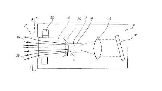
An exemplary embodiment of the device according to the invention is illustrated in
Fig. 1 wherein 10 denotes a frame made advantageously of Invar or another suitable
material, preferably one having a low coefficient of thermal expansion to minimi7~
misalignments of the optical system due to ambient temperature variations. Mounted on the
frame 10 are a diffraction grating element 12, a focusing lens 14 and a cylindrical graded
index (GRIN) lens 16. The latter is selected and disposed such as to correct an offset in the
focal length of the lens 14. The GRIN lens may actually be composed of two axially placed
20 GRIN lenses which may be separated by an optical spacer 17. In the example illustrated, the
lens 14 has an offset of +2% and the lens 16 is slightly shorter than a half-pitch 1:1
cylindrical GRIN lens to correct for the offset. Alternatively, but less preferably, an optically
equivalent GRIN lens arrangement can be used wherein two back-to-back substantially
quarter pitch GRIN lenses are coupled with their collim~ting ends such that a substantially
2s 1:1 im~ging iS provided for an image or beam at an end of the lens. The lens 16 has an
optical axis L which is colinear with the optical axis of the lens 14.
A glass concentrator block 18 is mounted adjacent the GRIN lens 16 and facing the
lens with its first end which is attached to the frame 10 with an epoxy adhesive 20 or other
30 suitable adhesive. Most epoxy adhesives are suitable for this purpose which will be
explained in more detail below. The concentrator has a funnel-like shape wherein the
CA 022~2130 1998-10-28
Doc.Nol0-88CA Patent
waveguides at one end (first end) have a narrower spacing than at the distal, second end.
This facilitates the ~tt~chment of fibers to the second end of the concentrator.
5 The distal (left-hand in the drawing), second end of the block 18 is fixed to a thermal
compensator 22 the details of which are shown in Fig. 2. The concentrator block 18 has a
number of waveguides therein, one of which is connected, with an optical adhesive, to an
input optical fiber 24 while the others are connected by the optical adhesive to output fibers
e.g. 26, 28.
As seen in Fig. 2, the concentrator 18 is fixed to the compensator 22 which has a
resistive heating element 30 with two leads 32 to a power supply, not shown. Thecompensator is attached to the frame 10, wherein a part of the length of the compensator is
not supported. This has the effect of the non-supported part expanding freely when heat is
generated by the heating element 30. This in turn causes the second end ofthe block 18 to
shift laterally (rightwise in Fig. 2). The adhesive attachment 20 is selected such as to enable
a small displacement of the joint. As a result, the block 18 moves pivotally about the first
end which is glued to the frame 10. The pivotal displacement is equivalent to an angular
displacement of the concentrator 18 relative to the optical axes of the lens 14 or the GRIN
20 lens 16.
The purpose of the design illustrated herein by way of example is to correct an offset in
alignment between the sub-beams generated by the grating 12, lens 14 and GRIN lens 16
from an input (e.g. multiplexed) beam when passed into system through the input fiber 24.
25 Such offset, as explained above, may occur when a temperature change is experienced on
various components of the device. To correct the offset, controlled heating is applied to the
heating element 30. The actuator 22 expands, and the concentrator 18 moves pivotally by an
angle typically less than 0.5 deg. As a result, the angle of the input beam (fiber 24) entering
the lenses 16, 14 and incident on the grating 12 changes sufficiently to cause the return sub-
30 beams to shift as well. The application of heat is controlled so that the sub-beams are aligned
with the respective waveguides of the concentrator 18.
CA 022~2130 1998-10-28
Doc.No10-88CA Patent
It is feasible to provide other actuating means for lateral displacement of the concentrator 18
than illustrated, with a view to adjusting the alignment of the sub-beams with the waveguides
of the concentrator 18. It will also be noted that the input beam does not have to be passed
5 through the concentrator, but rather from an independent source of light, whereby a lateral
rather than an angular displacement of the concentrator 18 may be employed. In such a case,
the adhesive attachment of the first end of the concentrator would not be necessary.